Anisotropic-strain-enhanced hole mobility in GaN by lattice matching to ZnGeN2 and MgSiN2
Abstract
The key obstacle toward realizing integrated gallium nitride (GaN) electronics is its low hole mobility. Here, we explore the possibility of improving the hole mobility of GaN via epitaxial matching to II-IV nitride materials that have recently become available, namely ZnGeN2 and MgSiN2. We perform state-of-the-art calculations of the hole mobility of GaN using the ab initio Boltzmann transport equation. We show that effective uniaxial compressive strain of GaN along the by lattice matching to ZnGeN2 and MgSiN2 results in the inversion of the heavy hole band and split-off hole band, thereby lowering the effective hole mass in the compression direction. We find that lattice matching to ZnGeN2 and MgSiN2 induces an increase of the room-temperature hole mobility by 50% and 260% as compared to unstrained GaN, respectively. Examining the trends as a function of strain, we find that the variation in mobility is highly nonlinear; lattice matching to a hypothetical solid solution of Zn0.75Ge0.75Mg0.25Si0.25N2 would already increase the hole mobility by 160%.
Wurtzite gallium nitride has become a fundamental semiconductor component in a variety of electronic and optical devices, including radio-frequency applicationsRunton et al. (2013); Zhang et al. (2021), power electronicsAmano et al. (2018), and light emitting diodes (LEDs)Nakamura, Senoh, and Mukai (1993); Nakamura et al. (1995); Li et al. (2016). Many remarkable properties of GaN can be traced back to its electronic structure. As a wide-gap semiconductor with a band gap of 3.4 eV at room temperatureBarker and Ilegems (1973); Madelung (1991), GaN can support higher voltages without experiencing field-induced breakdown when compared with Si. GaN can be alloyed with other nitride semiconductors such as AlNWu et al. (2004); Taniyasu, Kasu, and Makimoto (2006) and InNArif, Ee, and Tansu (2007); Neufeld et al. (2008) to tune the band gap between 0.6 and 6.2 eV, allowing for the realization of an array of materials for optoelectronic applications.
Electrons in GaN exhibit high room-temperature mobility, reaching up to 1000 cm2/VsNakamura, Mukai, and Senoh (1992); Götz et al. (1996, 1998); Kyle et al. (2014); Poncé, Jena, and Giustino (2019a, b); Jhalani et al. (2020) at low defect concentration. Conversely, hole carriers in GaN exhibit comparatively low mobility, usually below 31 cm2/VsRubin et al. (1994); Kozodoy et al. (1998, 2000); Arakawa et al. (2016); Horita et al. (2017); McLaurin and Speck (2007). The imbalance between electron and hole mobility hinders the application of GaN to integrated electronics based on complementary field-effect devices, and severely limits the uses of -channel GaN in power electronics and radio-frequency switchingAmano et al. (2018); Bader et al. (2020). In order to meet these technological demands, materials engineering approaches aimed at increasing the hole mobility of GaN are needed.
A common approach to improving the carrier mobility of semiconductors is via strain engineering. In the case of GaN, several experimental and theoretical/computational reports explored this possibility. Using perturbation theory, Suzuki et al. found that compressive uniaxial strain along the in-plane axis (see Fig. 1) induces the inversion of the heavy hole and split-off hole bandsSuzuki and Uenoyama (1996). The resulting valence-band maximum has a small effective mass along the direction, leading to increased hole mobility. Using an effective-mass-theory approach, Yeo et al. found that for growth in the (100) crystal orientation, strain induced in a GaN quantum well sandwiched between AlGaN layers would lead to a lighter effective mass along the compression directionYeo, Chong, and Li (1998). In recent experiments, Gupta et al. realized uniaxial compressive strain of GaN in the basal plane of the wurtzite structure (perpendicular to the axis, see Fig. 1) by using a fin geometry, while allowing for strain release in the other directionsGupta et al. (2019). This setup achieved a 25%-50% reduction in sheet resistance of -type GaN along the compressive uniaxial strain direction. Using the ab initio Boltzmann transport equation (aiBTE), Poncé et al. showed that imposing tensile biaxial strain in the (0001) plane, resulting in 2% compression along the axis, raises the split-off band above the heavy- and light-hole bands, thereby increasing the hole mobility along the same direction by 250%Poncé, Jena, and Giustino (2019a, b).
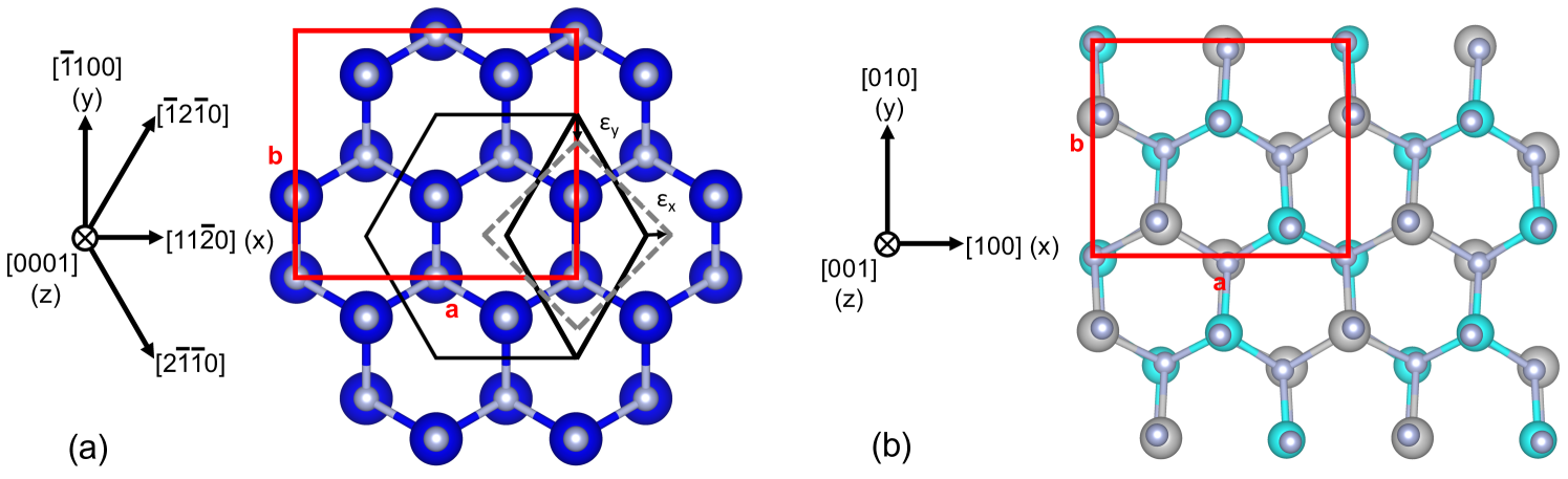
In this work, we explore an alternative strategy for improving the hole mobility of GaN via strain engineering. A possible route to inducing in-plane uniaxial strain perpendicular to the GaN crystal ([0001]) axis is via epitaxial growth of GaN on II-IV nitride materials with mismatched lattice parameters. Two candidate materials for this purpose are ZnGeN2 and MgSiN2, which crystallize in an orthorhombic lattice with space group Pna21. To discuss the relation between the lattice parameters of ZnGeN2, MgSiN2, and GaN, we use a common reference frame for the hexagonal and the orthorhombic lattices, as shown in Fig. 1. The correspondence between hexagonal and orthorhombic directions is provided in Table S1.
For ZnGeN2, a range of values has been reported for the room-temperature (300 K) lattice parameters along the and directions [see Fig. 1(b)]: 6.38-6.45 Å and 5.46-5.52 Å Blanton et al. (2017); Tellekamp et al. (2020). We consider the values 6.425 Å and 5.478 Å to be representative as averages over the experimentally measured lattice parameters and will proceed to use these to determine strain values. For MgSiN2, accurate x-ray and neutron diffraction measurements at room temperature indicate lattice constants Å and Å Bruls et al. (2000).
The lattice parameters of GaN in the orthorhombic cell outlined in Fig. 1(a) are = 6.364 Å and = 5.511 Å Gian, Skowronski, and Rohrer (1996); Tellekamp et al. (2020), therefore the epitaxial matching of GaN to ZnGeN2 and MgSiN2 will induce a tensile strain along the () direction, and a compressive strain along the () direction. For calculations of strained GaN, we impose the strain using the experimental room-temperature lattice parameters of GaN and the II-IV nitrides (see details in the supplementary material). The resulting strain values are listed in Table 1. Growth of ZnGeN2 on GaN has recently been demonstrated via molecular beam epitaxy Tellekamp et al. (2020), paving the way for the realization of devices based on strained GaN. Growth of GaN on MgSiN2 or MgSiN2 on GaN has not yet been explored. The effect of in-plane uniaxial strain on the mobility of GaN has been investigated theoretically using a variety of effective-mass modelsRode and Gaskill (1995); Look et al. (1997); Look and Molnar (1997); Abdel-Motaleb and Korotkov (2005), but these models predate recent developments in predictive ab initio calculations of carrier mobilitiesPoncé, Margine, and Giustino (2018); Poncé, Jena, and Giustino (2019a); Jhalani et al. (2020), hence a study using state-of-the-art computational techniques is warranted.
We perform density functional theory (DFT) calculatons, density functional perturbation theory (DFPT) calculations, and Wannier-Fourier interpolation of electronic structure, phonon dispersions, and electron-phonon coupling matrix elements using the Quantum ESPRESSO packageGiannozzi et al. (2017), the Wannier90 codeMostofi et al. (2014), and the EPW codeGiustino, Cohen, and Louie (2007); Noffsinger et al. (2010); Verdi and Giustino (2015); Poncé et al. (2016). We use the local density approximation (LDA)Ceperley and Alder (1980); Perdew and Zunger (1981) and optimized norm-conserving Vanderbilt (ONCV) pseudopotentialsHamann (2013); Schlipf and Gygi (2015). In order to obtain accurate band structures and effective masses, we employ the GW method as implemented in the Yambo codeMarini et al. (2009); Sangalli et al. (2019); Godby and Needs (1989), including spin-orbit coupling in the calculations. The calculation of carrier drift mobility is performed using the ab initio Boltzmann transport equationLi (2015); Madsen, Carrete, and Verstraete (2018) (aiBTE) and ultra-dense grids of wavevectors in the Brillouin zonePoncé, Margine, and Giustino (2018); Poncé et al. (2020, 2021); Brunin et al. (2020), as implemented in the EPW code. A detailed description of the computational setup is provided in the supplementary material.
We perform structural optimization of the unit cell parameters and internal coordinates of unstrained GaN. For strained GaN, we determine the strain configuration in the plane using the experimental lattice parameters of GaN, ZnGeN2, and MgSiN2, and we optimize the parameter as well as the internal coordinates, see Fig. 1. Detailed information about the structural parameters and strain levels considered is reported in Table S1 and Fig. S1. In the following we discuss three systems: unstrained GaN, and GaN strained to match ZnGeN2 (GaN@ZnGeN2) or MgSiN2 (GaN@MgSiN2) (Table 1).
| GaN@ZnGeN2Blanton et al. (2017); Tellekamp et al. (2020) | 0.96% | -0.60% |
|---|---|---|
| GaN@MgSiN2Bruls et al. (2000) | 1.72% | -4.33% |
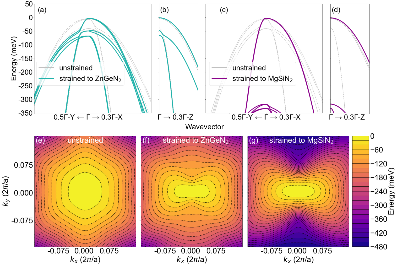
Figures 2(a)-(d) show the valence-band structure of unstrained and strained GaN near the band extremum. In panels (a) and (b) we compare unstrained GaN with GaN@ZnGeN2, and in panels (c) and (d) we compare unstrained GaN with GaN@MgSiN2. The reciprocal space lines X, Y, and Z are aligned with the corresponding Cartesian directions in real space, shown in Fig. 1. The strain induces an inversion of the heavy-hole band and of the split-off hole band along the compression direction Y, leading to a reduced effective mass in the same direction. The energy separation between the inverted bands along this direction is 50 meV for ZnGeN2, and 320 meV for MgSiN2. We note that this behavior is only observed for the compression direction, while band inversion does not occur along the directions of tensile strain (X and Z).
In Figs. 2(e)-(g) we show maps of the energy of the highest valence band of GaN, GaN@ZnGeN2, and GaN@MgSiN2 in the - plane, for . Panel (e) shows the expected six-fold symmetry of the band of unstrained GaN. Panels (f) and (g) show that strain reduces this symmetry and the map adopts the symmetries of the orthorhombic structure, with the steepest dispersion and lightest mass along the direction.
To quantify the change in effective masses, we calculate the curvature of the GW bands along the , , and directions using finite differences within 5 meV of the valence-band maximum. The results of these calculations are reported in Table 2, and methodological details are provided in the supplementary material. Unstrained GaN exhibits an effective mass along the X and Y directions, and along Z. These values are in agreement with previous GW calculationsPoncé, Jena, and Giustino (2019a). In the case of anisotropically strained GaN, we find lighter effective masses along the direction of compression, namely and for GaN@ZnGeN2 and GaN@MgSiN2. The electron effective masses can be found in Table S4 in the supplementary material.
| Direction | GaN | GaN@ZnGeN2 | GaN@MgSiN2 | |
|---|---|---|---|---|
| Holes | 0.48 | 1.57 | 1.62 | |
| 0.48 | 0.21 | 0.18 | ||
| 1.98 | 2.08 | 2.30 |
We note that we find significant non-parabolicity in the valence band frontier of GaN, as noted in previous theoretical calculationsRinke et al. (2008). In particular, a parabolic dispersion is found only within a 5 meV energy range from the valence band top in unstrained GaN. Below this energy, a band swap occurs and the heavy-hole band becomes the highest valence band. The valence bands of strained GaN@ZnGeN2 also display non-parabolicity: the bands within 50 meV of the maximum are split-off holes with low effective masses, while the bands below 50 meV are the heavy holes. A detailed analysis of the variation of the effective mass with energy is reported in Fig. S2.
We also checked the effect of strain on the phonon dispersion relations of GaN. Fig. S3 shows the change of the phonon band structures from unstrained GaN to GaN@ZnGeN2 and GaN@MgSiN2. As expected, the only significant changes are observed for GaN@MgSiN2, which carries the largest strain. In this case we find an 11% reduction in group velocity of transverse acoustic phonons along the compression direction, and a 2.5% increase in the longitudinal optical phonon energy.
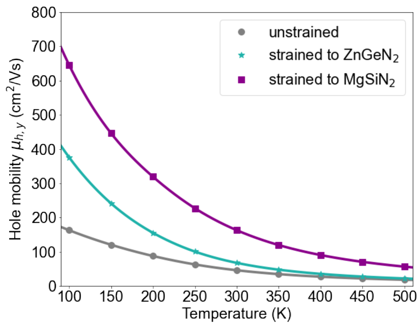
Our aiBTE calculations yield room-temperature hole mobilities along the and directions cm2/Vs, and direction cm2/Vs for unstrained GaN, in agreement with previous calculationsPoncé, Jena, and Giustino (2019a). Our results slightly exceed the mobility of 31 cm2/Vs measured on -type, ultra-low defect-density GaN samplesHorita et al. (2017). Upon application of strain, the mobility increases to cm2/Vs for GaN@ZnGeN2 (47% increase) and to cm2/Vs for GaN@MgSiN2 (255% increase). Temperature-dependent mobilities for all three cases are shown in Fig. 3.
Along the and directions, where the material experiences tensile strain, the hole mobility is only slightly changed: in the case of GaN@ZnGeN2, the mobility decreases by 12% along the direction and by 1% along the direction; in the case of GaN@MgSiN2, the mobility increases by 4% along and decreases by 7% along . The temperature-dependent mobilities along the and directions are shown in Figs. S4 and S5. We have also analyzed electron mobilities, but due to the largely isotropic nature of the conduction band, the values for GaN@ZnGeN2and GaN@MgSiN2 show only minor deviations from the values in unstrained GaN (see supplementary material).
The mobility is mostly dictated by the band dispersions, which have been discussed above, and the carrier scattering rates. We analyze the most representative electron-phonon scattering ratesPoncé, Schlipf, and Giustino (2019) by considering holes located at meV below the valence-band maximum, with K. To do so, we perform a spectral decomposition of the angular-averaged scattering rate by phonon energy (see Fig. S6). For unstrained and strained GaN the trends are consistent: we find that 80% of the scattering rate originates from acoustic phonon scattering, and in particular piezoacoustic scattering. Scattering by longitudinal-optical phonons account for 15% of the total scattering rate, and scattering by transverse-optical phonons accounts for the remaining 5%. The scattering rates as a function of energy from the valence band edge are reported in Supplemental Fig. S7, and their values at are reported in Table 3. We see that the scattering rates are much less sensitive to strain than the effective masses, therefore the main source of mobility enhancement is the decrease in the hole mass.
It is instructive to compare our mobility in the compressive direction from aiBTE calculations with the trends that one obtains from a simple Drude model, with values reported in Table 3. While the trends in the Drude mobilities are similar to the aiBTE results, the Drude values are off by a factor of two. We attribute this to the fact that the valence-band structures of GaN@ZnGeN2 and GaN@MgSiN2 display significant anisotropy and a complex, non-parabolic structure; a first-principles treatment is therefore required to accurately describe hole transport in strained GaN systems.
| GaN | GaN@ZnGeN2 | GaN@MgSiN2 | ||
| () | 0.48 | 0.21 | 0.18 | |
| (THz) | 54.0 | 59.2 | 43.9 | |
| (cm2/Vs) | Drude | 68 | 141 | 223 |
| aiBTE | 46 | 67 | 163 |
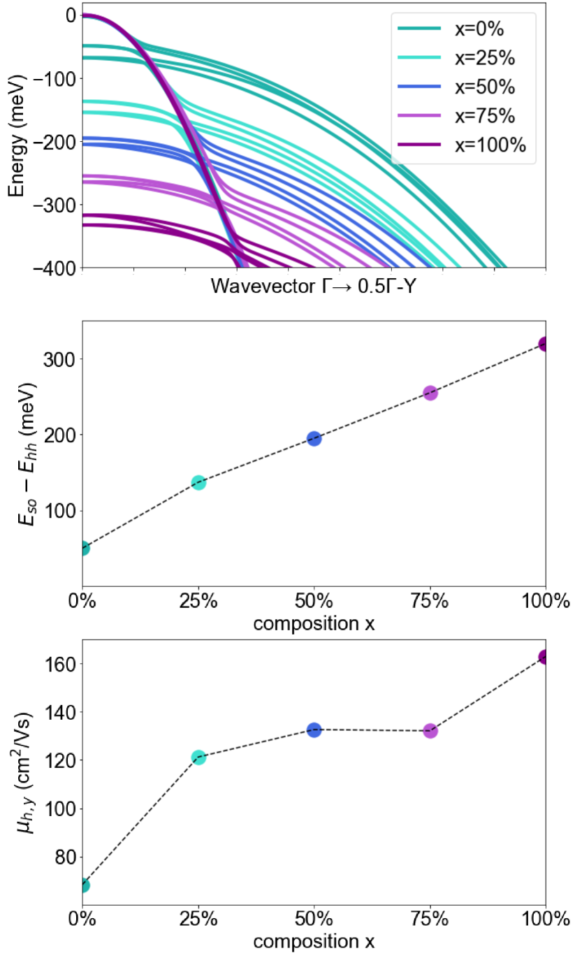
The strain values for GaN@ZnGeN2 are modest and should allow for pseudomorphic growth of GaN layers of sufficient thickness for device structures. The GaN@MgSiN2 values are probably too large to allow for growth of device structures; we are including MgSiN2 to establish trends, and in the eventuality that partially relaxed or alloyed layers based on MgSiN2 could be used in structures with a smaller mismatch. Given that the mobility enhancement in GaN@ZnGeN2 is modest, and that the more appealing GaN@MgSiN2 may be difficult to realize due to the high strain, we also considered the possibility of modifying the lattice parameters of ZnGeN2 through alloying. In this context, we assess the potential of hypothetical solid solutions of Zn1-xGe1-xMgxSixN2. Figure 4(a) shows how the band structure of GaN evolves under increasing strain from to . As expected, with increasing compressive strain the heavy hole band is further lowered in energy, thereby increasing the energy separation between the split-off holes and the heavy holes, as shown in Fig. 4(b). However, while the energy separation between split-off holes and heavy holes is linear in the strain, we find that the hole mobility varies nonlinearly, and tends to saturate near . At the hole mobility in the direction is already as high as 121 cm2/Vs, which is more than 160% higher than in unstrained GaN.
Finally, the effects of including the long-range quadruple moment, omitted in this work, in interpolating the electron-phonon matrix elements in GaN have been previously exploredJhalani et al. (2020); Park et al. (2020); Brunin et al. (2020); Poncé et al. (2021). It was shown that the mobility of GaN increases from 45 cm2/Vs to 55 cm2/Vs when including quadrupole corrections (22% increase). We demonstrate that the scattering physics across strain states remains consistent, and the increase in hole mobilities is driven by the change in band dispersions under strain. The inclusion of the long-range quadruple would thus scale the mobilities upwards, but we anticipate the trends with strain to remain the same. We have additionally tested the influence of including long-range quadruples moments in the interpolation on the calculated hole mobility in unstrained GaN and found an increase to 53 cm2/Vs from 47 cm2/Vs, in agreement with previous studies.
In summary, using state-of-the-art first-principles calculations and the ab initio Boltzmann transport equation, we investigated the possibility of increasing the room-temperature hole mobility of GaN through anisotropic in-plane strain via pseudomorphic epitaxial growth on ZnGeN2 and MgSiN2. We found that GaN@ZnGeN2 can lead to an increase in the hole mobility along the direction of compression from 46 cm2/Vs in unstrained GaN to 76 cm2/Vs, and GaN@MgSiN2 can increase the mobility up to 163 cm2/Vs. Due to the nonlinear dependence of mobility on strain, a hypothetical solid solution of 25% MgSiN2 added to ZnGeN2 would already increase the hole mobility to 121 cm2/Vs. Beyond strain engineering -channel GaN devices, growth of effectively uniaxial compressed GaN on II-IV nitrides could pose a promising route for engineering monolithic GaN complementary metal–oxide–semiconductor (CMOS) devices. We hope that the present study will motivate renewed experimental efforts toward the realization of high-mobility -type GaN.
This research is supported by the Computational Materials Sciences Program funded by the U.S. Department of Energy (DOE), Office of Science, Basic Energy Sciences BES), under Award No. DE-SC0020129 (J.L.: calculations and data analysis, manuscript preparation; F.G.: project supervision, manuscript preparation). S.P. acknowledges support from the F.R.S.-FNRS and the Consortium des Équipements de Calcul Intensif (CÉCI). Work by N.L.A. was supported by the Army Research Office (W911NF-16-1-0538). Work by C.G.VdW. was supported by the US DOE, Office of Science, BES, under Award No. DE-SC0010689. The authors acknowledge the Texas Advanced Computing Center (TACC) at The University of Texas at Austin for providing HPC resources, including the Frontera and Lonestar5 systems, that have contributed to the research results reported within this paper. URL: http://www.tacc.utexas.edu. This research used resources of the National Energy Research Scientific Computing Center, a DOE Office of Science User Facility supported by the Office of Science of the U.S. Department of Energy under Contract No. DE-AC02-05CH11231. Finally, this material is based upon work supported by the National Science Foundation under OAC Grant No. 2103991 (software development, J.L.).
I Supplementary Material
Supporting information, including full calculation details and additional data, can be found in the Supplementary Materials document.
Conflicts of Interest
The authors have no conflicts of interest to disclose
Data Availability Statement
The data that support the findings of this study are available from the corresponding author upon reasonable request.
References
- Runton et al. (2013) D. W. Runton, B. Trabert, J. B. Shealy, and R. Vetury, “History of GaN: high-power rf gallium nitride (GaN) from infancy to manufacturable process and beyond,” IEEE Microw. Mag 14, 82–93 (2013).
- Zhang et al. (2021) Y. Zhang, A. Zubair, Z. Liu, M. Xiao, J. Perozek, Y. Ma, and T. Palacios, “GaN FinFETs and trigate devices for power and RF applications: review and perspective,” Semicond. Sci. Technol. 36, 054001 (2021).
- Amano et al. (2018) H. Amano, Y. Baines, E. Beam, M. Borga, T. Bouchet, P. R. Chalker, M. Charles, K. J. Chen, N. Chowdhury, R. Chu, C. D. Santi, M. M. D. Souza, S. Decoutere, L. D. Cioccio, B. Eckardt, T. Egawa, P. Fay, J. J. Freedsman, L. Guido, O. Häberlen, G. Haynes, T. Heckel, D. Hemakumara, P. Houston, J. Hu, M. Hua, Q. Huang, A. Huang, S. Jiang, H. Kawai, D. Kinzer, M. Kuball, A. Kumar, K. B. Lee, X. Li, D. Marcon, M. März, R. McCarthy, G. Meneghesso, M. Meneghini, E. Morvan, A. Nakajima, E. M. S. Narayanan, S. Oliver, T. Palacios, D. Piedra, M. Plissonnier, R. Reddy, M. Sun, I. Thayne, A. Torres, N. Trivellin, V. Unni, M. J. Uren, M. V. Hove, D. J. Wallis, J. Wang, J. Xie, S. Yagi, S. Yang, C. Youtsey, R. Yu, E. Zanoni, S. Zeltner, and Y. Zhang, “The 2018 GaN power electronics roadmap,” J. Phys. D Appl. Phys. 51, 163001 (2018).
- Nakamura, Senoh, and Mukai (1993) S. Nakamura, M. Senoh, and T. Mukai, “p-GaN/n-InGaN/n-GaN double-heterostructure blue-light-emitting diodes,” Jpn. J. Appl. Phys. 32, L8–L11 (1993).
- Nakamura et al. (1995) S. Nakamura, M. Senoh, N. Iwasa, and S. Nagahama, “High-brightness InGaN blue, green and yellow light-emitting diodes with quantum well structures,” Jpn. J. Appl. Phys. 34, L797–L799 (1995).
- Li et al. (2016) G. Li, W. Wang, W. Yang, Y. Lin, H. Wang, Z. Lin, and S. Zhou, “GaN-based light-emitting diodes on various substrates: a critical review,” Rep. Prog. Phys 79, 056501 (2016).
- Barker and Ilegems (1973) A. S. Barker and M. Ilegems, “Infrared lattice vibrations and free-electron dispersion in GaN,” Phys. Rev. B 7, 743–750 (1973).
- Madelung (1991) O. Madelung, ed., Semiconductors: group IV elements and III-V compounds (Springer-Verlag Berlin Heidelberg, 1991).
- Wu et al. (2004) S. Wu, V. Adivarahan, M. Shatalov, A. Chitnis, W.-H. Sun, and M. A. Khan, “Micro-pixel design milliwatt power 254 nm emission light emitting diodes,” Jpn. J. Appl. Phys. 43, L1035–L1037 (2004).
- Taniyasu, Kasu, and Makimoto (2006) Y. Taniyasu, M. Kasu, and T. Makimoto, “An aluminium nitride light-emitting diode with a wavelength of 210 nanometres,” Nature 441, 325–328 (2006).
- Arif, Ee, and Tansu (2007) R. A. Arif, Y.-K. Ee, and N. Tansu, “Polarization engineering via staggered InGaN quantum wells for radiative efficiency enhancement of light emitting diodes,” Appl. Phys. Lett. 91, 091110 (2007).
- Neufeld et al. (2008) C. J. Neufeld, N. G. Toledo, S. C. Cruz, M. Iza, S. P. DenBaars, and U. K. Mishra, “High quantum efficiency InGaN/GaN solar cells with 2.95 eV band gap,” Appl. Phys. Lett. 93, 143502 (2008).
- Nakamura, Mukai, and Senoh (1992) S. Nakamura, T. Mukai, and M. Senoh, “Si- and Ge-doped GaN films grown with GaN buffer layers,” Jpn. J. Appl. Phys. 31, 2883–2888 (1992).
- Götz et al. (1996) W. Götz, N. M. Johnson, C. Chen, H. Liu, C. Kuo, and W. Imler, “Activation energies of Si donors in GaN,” Appl. Phys. Lett. 68, 3144–3146 (1996).
- Götz et al. (1998) W. Götz, L. T. Romano, J. Walker, N. M. Johnson, and R. J. Molnar, “Hall-effect analysis of GaN films grown by hydride vapor phase epitaxy,” Appl. Phys. Lett. 72, 1214–1216 (1998).
- Kyle et al. (2014) E. C. H. Kyle, S. W. Kaun, P. G. Burke, F. Wu, Y.-R. Wu, and J. S. Speck, “High-electron-mobility GaN grown on free-standing GaN templates by ammonia-based molecular beam epitaxy,” J. Appl. Phys. 115, 193702 (2014).
- Poncé, Jena, and Giustino (2019a) S. Poncé, D. Jena, and F. Giustino, “Hole mobility of strained GaN from first principles,” Phys. Rev. B 100, 085204 (2019a).
- Poncé, Jena, and Giustino (2019b) S. Poncé, D. Jena, and F. Giustino, “Route to high hole mobility in GaN via reversal of crystal-field splitting,” Phys. Rev. Lett. 123, 096602 (2019b).
- Jhalani et al. (2020) V. A. Jhalani, J.-J. Zhou, J. Park, C. E. Dreyer, and M. Bernardi, “Piezoelectric electron-phonon interaction from ab initio dynamical quadrupoles: impact on charge transport in wurtzite GaN,” Phys. Rev. Lett. 125, 136602 (2020).
- Rubin et al. (1994) M. Rubin, N. Newman, J. S. Chan, T. C. Fu, and J. T. Ross, “P-type gallium nitride by reactive ion-beam molecular beam epitaxy with ion implantation, diffusion, or coevaporation of Mg,” Appl. Phys. Lett. 64, 64–66 (1994).
- Kozodoy et al. (1998) P. Kozodoy, S. Keller, S. DenBaars, and U. Mishra, “MOVPE growth and characterization of Mg-doped GaN,” J. Cryst. Growth 195, 265–269 (1998).
- Kozodoy et al. (2000) P. Kozodoy, H. Xing, S. P. DenBaars, U. K. Mishra, A. Saxler, R. Perrin, S. Elhamri, and W. C. Mitchel, “Heavy doping effects in Mg-doped GaN,” J. Appl. Phys. 87, 1832–1835 (2000).
- Arakawa et al. (2016) Y. Arakawa, K. Ueno, A. Kobayashi, J. Ohta, and H. Fujioka, “High hole mobility p-type GaN with low residual hydrogen concentration prepared by pulsed sputtering,” APL Materials 4, 086103 (2016).
- Horita et al. (2017) M. Horita, S. Takashima, R. Tanaka, H. Matsuyama, K. Ueno, M. Edo, T. Takahashi, M. Shimizu, and J. Suda, “Hall-effect measurements of metalorganic vapor-phase epitaxy-grown p-type homoepitaxial GaN layers with various mg concentrations,” Jpn. J. Appl. Phys. 56, 031001 (2017).
- McLaurin and Speck (2007) M. McLaurin and J. S. Speck, “p-type conduction in stacking-fault-free m -plane gan,” Phys. Status Solidi RRL 1, 110–112 (2007).
- Bader et al. (2020) S. J. Bader, H. Lee, R. Chaudhuri, S. Huang, A. Hickman, A. Molnar, H. G. Xing, D. Jena, H. W. Then, N. Chowdhury, and T. Palacios, “Prospects for wide bandgap and ultrawide bandgap cmos devices,” IEEE Transactions on Electron Devices 67, 4010–4020 (2020).
- Suzuki and Uenoyama (1996) M. Suzuki and T. Uenoyama, “Strain effect on electronic and optical properties of GaN/AlGaN quantum-well lasers,” J. Appl. Phys. 80, 6868–6874 (1996).
- Yeo, Chong, and Li (1998) Y. Yeo, T. Chong, and M. Li, “Effect of the (100) crystal orientation on the optical gain of wurtzite GaN-AlGaN quantum-well lasers,” IEEE J. Quantum Electron. 34, 1270–1279 (1998).
- Gupta et al. (2019) C. Gupta, Y. Tsukada, B. Romanczyk, S. S. Pasayat, D.-A. James, E. Ahmadi, S. Keller, and U. K. Mishra, “First demonstration of improvement in hole conductivity in c-plane III-nitrides through application of uniaxial strain,” Jpn. J. Appl. Phys. 58, 030908 (2019).
- Blanton et al. (2017) E. W. Blanton, K. He, J. Shan, and K. Kash, “Characterization and control of ZnGeN2 cation lattice ordering,” J. Cryst. Growth 461, 38–45 (2017).
- Tellekamp et al. (2020) M. B. Tellekamp, C. L. Melamed, A. G. Norman, and A. Tamboli, “Heteroepitaxial integration of ZnGeN2 on GaN buffers using molecular beam epitaxy,” Cryst. Growth Des. 20, 1868–1875 (2020).
- Bruls et al. (2000) R. Bruls, H. Hintzen, R. Metselaar, and C.-K. Loong, “Anisotropic thermal expansion of MgSiN2 from 10 to 300k as measured by neutron diffraction,” J. Phys. Chem. Solids 61, 1285–1293 (2000).
- Gian, Skowronski, and Rohrer (1996) W. Gian, M. Skowronski, and G. S. Rohrer, “Structural defects and their relationship to nucleation of GaN thin films,” MRS Proceedings 423, 475 (1996).
- Rode and Gaskill (1995) D. L. Rode and D. K. Gaskill, “Electron hall mobility of n-GaN,” Appl. Phys. Lett. 66, 1972–1973 (1995).
- Look et al. (1997) D. C. Look, D. C. Reynolds, J. W. Hemsky, J. R. Sizelove, R. L. Jones, and R. J. Molnar, “Defect donor and acceptor in GaN,” Phys. Rev. Lett. 79, 2273–2276 (1997).
- Look and Molnar (1997) D. C. Look and R. J. Molnar, “Degenerate layer at GaN/sapphire interface: influence on hall-effect measurements,” Appl. Phys. Lett. 70, 3377–3379 (1997).
- Abdel-Motaleb and Korotkov (2005) I. M. Abdel-Motaleb and R. Y. Korotkov, “Modeling of electron mobility in GaN materials,” J. Appl. Phys. 97, 093715 (2005).
- Poncé, Margine, and Giustino (2018) S. Poncé, E. R. Margine, and F. Giustino, “Towards predictive many-body calculations of phonon-limited carrier mobilities in semiconductors,” Phys. Rev. B 97, 121201 (2018).
- Giannozzi et al. (2017) P. Giannozzi, O. Andreussi, T. Brumme, O. Bunau, M. B. Nardelli, M. Calandra, R. Car, C. Cavazzoni, D. Ceresoli, M. Cococcioni, N. Colonna, I. Carnimeo, A. D. Corso, S. de Gironcoli, P. Delugas, R. A. DiStasio, A. Ferretti, A. Floris, G. Fratesi, G. Fugallo, R. Gebauer, U. Gerstmann, F. Giustino, T. Gorni, J. Jia, M. Kawamura, H.-Y. Ko, A. Kokalj, E. Küçükbenli, M. Lazzeri, M. Marsili, N. Marzari, F. Mauri, N. L. Nguyen, H.-V. Nguyen, A. O. de-la Roza, L. Paulatto, S. Poncé, D. Rocca, R. Sabatini, B. Santra, M. Schlipf, A. P. Seitsonen, A. Smogunov, I. Timrov, T. Thonhauser, P. Umari, N. Vast, X. Wu, and S. Baroni, “Advanced capabilities for materials modelling with quantum ESPRESSO,” J. Phys. Condens. Matter 29, 465901 (2017).
- Mostofi et al. (2014) A. A. Mostofi, J. R. Yates, G. Pizzi, Y.-S. Lee, I. Souza, D. Vanderbilt, and N. Marzari, “An updated version of wannier90: A tool for obtaining maximally-localised Wannier functions,” Comput. Phys. Commun. 185, 2309–2310 (2014).
- Giustino, Cohen, and Louie (2007) F. Giustino, M. L. Cohen, and S. G. Louie, “Electron-phonon interaction using Wannier functions,” Phys. Rev. B 76, 165108 (2007).
- Noffsinger et al. (2010) J. Noffsinger, F. Giustino, B. D. Malone, C.-H. Park, S. G. Louie, and M. L. Cohen, “Epw: A program for calculating the electron–phonon coupling using maximally localized Wannier functions,” Comput. Phys. Commun. 181, 2140–2148 (2010).
- Verdi and Giustino (2015) C. Verdi and F. Giustino, “Fröhlich electron-phonon vertex from first principles,” Phys. Rev. Lett. 115, 176401 (2015).
- Poncé et al. (2016) S. Poncé, E. Margine, C. Verdi, and F. Giustino, “EPW: electron–phonon coupling, transport and superconducting properties using maximally localized Wannier functions,” Comp. Phys. Comm. 209, 116 – 133 (2016).
- Ceperley and Alder (1980) D. M. Ceperley and B. J. Alder, “Ground state of the electron gas by a stochastic method,” Phys. Rev. Lett. 45, 566–569 (1980).
- Perdew and Zunger (1981) J. P. Perdew and A. Zunger, “Self-interaction correction to density-functional approximations for many-electron systems,” Phys. Rev. B 23, 5048–5079 (1981).
- Hamann (2013) D. R. Hamann, “Optimized norm-conserving vanderbilt pseudopotentials,” Phys. Rev. B 88, 085117 (2013).
- Schlipf and Gygi (2015) M. Schlipf and F. Gygi, “Optimization algorithm for the generation of oncv pseudopotentials,” Computer Physics Communications 196, 36–44 (2015).
- Marini et al. (2009) A. Marini, C. Hogan, M. Grüning, and D. Varsano, “yambo: an ab initio tool for excited state calculations,” Comput. Phys. Commun. 180, 1392–1403 (2009).
- Sangalli et al. (2019) D. Sangalli, A. Ferretti, H. Miranda, C. Attaccalite, I. Marri, E. Cannuccia, P. Melo, M. Marsili, F. Paleari, A. Marrazzo, G. Prandini, P. Bonfà, M. O. Atambo, F. Affinito, M. Palummo, A. Molina-Sánchez, C. Hogan, M. Grüning, D. Varsano, and A. Marini, “Many-body perturbation theory calculations using the yambo code,” J. Phys. Condens. Matter 31, 325902 (2019).
- Godby and Needs (1989) R. W. Godby and R. J. Needs, “Metal-insulator transition in kohn-sham theory and quasiparticle theory,” Phys. Rev. Lett. 62, 1169–1172 (1989).
- Li (2015) W. Li, “Electrical transport limited by electron-phonon coupling from Boltzmann transport equation: an ab initio study of Si, Al, and MoS2,” Phys. Rev. B 92, 075405 (2015).
- Madsen, Carrete, and Verstraete (2018) G. K. Madsen, J. Carrete, and M. J. Verstraete, “Boltztrap2, a program for interpolating band structures and calculating semi-classical transport coefficients,” Comput. Phys. Commun. 231, 140–145 (2018).
- Poncé et al. (2020) S. Poncé, W. Li, S. Reichardt, and F. Giustino, “First-principles calculations of charge carrier mobility and conductivity in bulk semiconductors and two-dimensional materials,” Rep. Prog. Phys. 83, 036501 (2020).
- Poncé et al. (2021) S. Poncé, F. Macheda, E. R. Margine, N. Marzari, N. Bonini, and F. Giustino, “First-principles predictions of Hall and drift mobilities in semiconductors,” Phys. Rev. Research 3, 043022 (2021).
- Brunin et al. (2020) G. Brunin, H. P. C. Miranda, M. Giantomassi, M. Royo, M. Stengel, M. J. Verstraete, X. Gonze, G.-M. Rignanese, and G. Hautier, “Electron-phonon beyond Fröhlich: dynamical quadrupoles in polar and covalent solids,” Phys. Rev. Lett. 125, 136601 (2020).
- Rinke et al. (2008) P. Rinke, M. Winkelnkemper, A. Qteish, D. Bimberg, J. Neugebauer, and M. Scheffler, “Consistent set of band parameters for the group-iii nitrides aln, gan, and inn,” Phys. Rev. B 77, 075202 (2008).
- Poncé, Schlipf, and Giustino (2019) S. Poncé, M. Schlipf, and F. Giustino, “Origin of low carrier mobilities in halide perovskites,” ACS Energy Letters 4, 456–463 (2019).
- Park et al. (2020) J. Park, J.-J. Zhou, V. A. Jhalani, C. E. Dreyer, and M. Bernardi, “Long-range quadrupole electron-phonon interaction from first principles,” Phys. Rev. B 102, 125203 (2020).