Massively Scalable Wavelength Diverse Integrated Photonic Linear Neuron
Abstract
As computing resource demands continue to escalate in the face of big data, cloud-connectivity and the internet of things, it has become imperative to develop new low-power, scalable architectures. Neuromorphic photonics, or photonic neural networks, have become a feasible solution for the physical implementation of efficient algorithms directly on-chip. This application is primarily due to the linear nature of light and the scalability of silicon photonics, specifically leveraging the wide-scale complementary metal-oxide-semiconductor (CMOS) manufacturing infrastructure used to fabricate microelectronics chips. Current neuromorphic photonic implementations stem from two paradigms: wavelength coherent and incoherent. Here, we introduce a novel architecture that supports coherent and incoherent operation to increase the capability and capacity of photonic neural networks with a dramatic reduction in footprint compared to previous demonstrations. As a proof-of-principle, we experimentally demonstrate simple addition and subtraction operations on a foundry-fabricated silicon photonic chip. Additionally, we experimentally validate an on-chip network to predict the logical 2-bit gates AND, OR, and XOR to accuracies of and , respectively. This architecture is compatible with highly wavelength parallel sources, enabling massively scalable photonic neural networks.
1 Introduction
In recent years, integrated photonics has emerged as a viable and highly appealing candidate for neural network hardware implementation. Photonic neural networks (PNN) hold particular promise compared to traditional electronic implementations due to the highly favorable physical properties of photons compared to electrons for performing linear operations; namely, (i) the bosonic nature of light permits high degrees of parallelism in spatial mode and wavelength, (ii) such linear transformations are naturally implemented using standard photonic elements (i.e., beamsplitters and phase shifters) at the speed of light, and (iii) these operations can consume orders of magnitude less energy than their electronic counterparts [1, 2, 3, 4, 5]. In particular, silicon photonics provides an ideal platform for PNNs due to its compatibility with the standard complementary metal-oxide-semiconductor (CMOS) infrastructure used to fabricate microelectronic chips and the high index contrast between silicon and silicon dioxide which permits unparalleled device density [3]. Numerous approaches to optical neural networks have been demonstrated in various platforms, including as spiking [6, 7], phase-change materials [8, 9, 10], metal-sulfide microfibers [11, 12], photoelectric multiplication [13, 10], and semiconductor optical amplifiers [14, 15]. However, two primary categories have emerged for PNNs in the silicon photonics platform: wavelength coherent and incoherent [3].
Wavelength coherent designs rely on careful placement and tuning of Mach-Zehnder interferometers (MZI), such that optical interference provides the multiplication and summation operations. Carefully designed MZI mesh circuits can implement any real-valued matrix on-chip by reconfiguring phase shifters according to singular value decomposition [1, 16]. The coherent optical linear neuron (COLN) architecture implements vector-vector multiplication and summation by leveraging MZIs as inputs and weights for multiplication and coherent interference as the summation operator [17, 18]. Wavelength incoherent designs rely on multi-wavelength operation, often employing a broadband photodetector to perform summation, but through this method the phase of the signal is lost to optical-electrical conversion. For example, in the “Broadcast & Weight” protocol, multiple wavelength channels are launched as inputs along the same waveguide, which allows for parallel weighting with micro-ring resonator weight banks [19]. A balanced photodetector pair sums the vector-vector multiplication; however, multiple micro-ring weight banks can operate in parallel for vector-matrix operation, as demonstrated in [20].
In this work, we present a novel architecture that leverages both coherent and incoherent aspects to create a massively scalable PNN specific linear operator. This architecture requires fewer components, provides orders-of-magnitude footprint reduction, and consumes substantially less power than comparable designs. As an initial proof-of-principle, we experimentally demonstrate simple addition and subtraction on-chip. Additionally, we implement and demonstrate a neural network task on-chip, designed to perform logic gate operations (AND, OR, and XOR). Due to the compact footprint, low energy consumption, and scalability of the demonstrated linear neuron, these results pave the way toward large-scale PNNs with hundreds to thousands of neurons on a single silicon chip.
2 Proposed Architecture
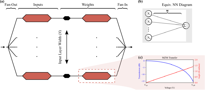
We begin our design derivation with inspiration from the COLN [17]. The operating principle of the COLN employs four key stages: Fan-Out, Input, Weighting, and Fan-In, as shown in Figure 1(a). At the Fan-Out, a continuous-wave (CW) optical carrier signal is split onto copies. Here, the Input and Weight stage is represented by amplitude modulators, which are implemented in hardware as Mach-Zehnder Modulators (MZM) and impose the inputs and weights onto the CW carrier signal. This signal is recombined from paths down to 1 path, performing summation of the input/weight products at the Fan-In through constructive interference. Figure 1(b) demonstrates the equivalent neural network (NN) diagram for this circuit, which performs the linear summation of the inputs multiplied by the synaptic weights, preparing the carrier signal for the activation stage. This optical circuit and the NN both reduce to the general form:
| (1) |
where, for the optical circuit, is the electric field output, as the number of layers in the width (or Fan-Out), is the weight vector, and is the input vector. In this formulation, and are represented by the electro-optic transfer function of the MZM in each layer similar to that seen in Figure 1(c). A key feature of the COLN circuit is that the output is in a state which, with minimal additional passive circuitry, is fully compatible both with an activation based on optical-electrical (OE), electrical processing, and electrical-optical (EO) conversion [21], direct optical-electrical-optical (OEO) activation [22] or all-optical, non-linear activation [23, 24].
In a fiber-optic based system, phase-shifters and splitters are readily available off-the-shelf [17]. However, when attempting to scale these down for an integrated photonic system, the size of MZM translates into a practical barrier. Current PN diode, free-carrier MZM devices each occupy a physical space of mm2 in on-chip area, severely limiting the scalabilty of this architecture. The first on-chip demonstration of the COLN in a silicon photonic chip utilizes a mm2 chip to implement a input/weight linear neuron, implementing the weights with thermal phase shifters, which are dramatically smaller at the cost of update speed [25, 26].
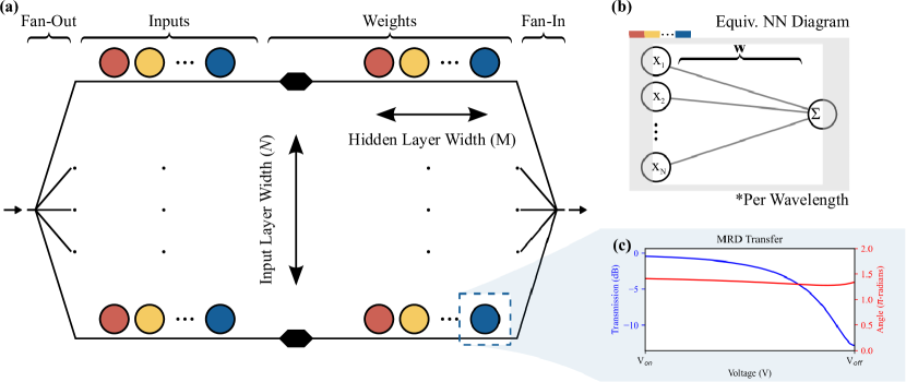
Our circuit architecture, which we subsequently refer to as Wavelength Diverse Integrated Photonic Linear Neuron (WDIPLN), begins as a COLN with naïve replacement of MZMs with micro-resonant devices (MRD), either micro-ring resonators or a micro-disks, as shown in Figure 2(a). With MRDs, we immediately benefit from the decrease in footprint. Single-channel MRDs are commonly m2 in size [27]. In addition, careful design of the MRD allows for a desirable adaptation of the previous electro-optic transfer function, displayed in Figure 2(c). The MRD acts as an amplitude filter both in the input and weight stage of the network, for each bus in the layer width. MRDs are sensitive, but if the coupling condition is designed to be slightly under-coupled, it is possible to mitigate some of the phase sensitivity (for example, a depletion biased MRD would remain under-coupled during operation). This enables the coherent summation at the Fan-In stage to remain relatively stable for each channel.
Naïve WDIPLN introduces a feature beyond the COLN, namely wavelength diversity. For sufficiently small radii MRD (or, conversely, sufficiently large free-spectral-range (FSR)), we can place additional MRDs at new resonant wavelengths (or along specific channels, similar to wavelength-division-multiplexing (WDM) in optical communications). For example, in silicon photonics a suffiently large channel spacing has been demonstrated with a m radius microdisk modulator, with m, full width at half maximum of nm, and high quality factor (), which indicates high channel isolation [27].
Recently, a similar WDM scheme was proposed using MZMs, but the WDIPLN implementation with ring resonators have the advantage that the wavelength multiplexing/de-multiplexing is done intrinsically using the single device in a compact footprint [18]. We show a schematic for the naïve WDIPLN in Figure 2(a). This enables wavelength diverse operation of the coherent circuit at each wavelength channel, such that we have an incoherent circuit which acts like a coherent operator at each channel (), with a slight adaptation of Equation 1 to
| (2) |
We can claim Equation 2 for WDIPLN design with sufficiently isolated channels, where the interaction of each resonance occurs only in and around that wavelength. As discussed above, this is achieved by using sufficiently small MRDs with large FSRs. Using isolated wavelength channels enables the resonant based circuit to act as any individual COLN circuit for where here represents the number of wavelength channels in operation and the number of COLN circuits represented by a single WDIPLN circuit. Therefore, this design not only leverages smaller footprint devices, but enables further footprint reduction of a given system of linear neurons from the limit of one optical circuit per preceptron to one optical circuit per fully connected multi-layer perceptron (MLP) by using the input/weight pairs at each wavelength as shown in Figure 2(b).
In the naïve case, we have simply swapped each MZM with an MRD, such that the circuit requires MRDs, for layer width and wavelength channels (or layer depth) . This case is the same as using COLN circuits, which is equivalent only in abstracted device count complexity. Thus, an actual network with COLNs would require copies of the circuit resulting in a larger implementation.
| Architecture | COLN | COLN | WDIPLN | WDIPLN |
|---|---|---|---|---|
| (variation) | (nominal) | (w/ thermal MZI) | (naïve) | (nominal) |
| Input Element | MZM | MZM | Small MRD | Large MRD |
| Approx. Element Size (mm2) | ||||
| Weight Element | MZM | Thermal MZI | Small MRD | Small MRD |
| Approx. Element Size (mm2) | ||||
| Scaling Rule | ||||
| Physical Size (mm2) | Component Size Only (no routing considered) | |||
| Electrical I/O | Consider 4 Electrical I/O per element (2 EO, 2 Thermal) | |||
| Power Consumption (mW) | Same Configuration (2 EO, 2 Thermal) | |||
| EO Power - () | ||||
| Thermal Power - () | ||||
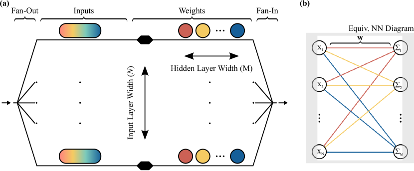
However, we recognize that the input stage MRDs are redundant. Therefore, to realize full WDIPLN we replace all input MRDs for a given layer with a carefully designed, larger radius MRD with an FSR that matches the channel spacing, as outlined in Figure 3(a). This adjustment lowers the total device count to which represents a dramatic improvement in device count scalability in addition to the physical size. As seen in Figure 3(b), the WDIPLN circuit in this form represents the linear weighting and summation stage of a fully connected MLP. A caveat of the fully-realized WDIPLN architecture is the inability to realize phase shifting per weight. In this way, we must limit the weight attribution to or . The phase shifters in this architecture are here as a global change to all weights simultaneously, serving both as path balancing and switching between subtractive or additive behavior. Table 1 summarizes the key differences between the COLN and WDIPLN, including scaling rules, physical size, electrical I/O, and power consumption estimates from available foundry process design kits (PDKs) [28, 29, 30]. We note that the physical size is calculated purely as fundamental device area, although both the COLN and WDIPLN require additional optical and electrical routing to connect to the outside world. This routing footprint was omitted from the total since it is highly implementation-specific and depends heavily on packaging constraints (i.e., edge coupled versus grating coupled, flip-chip bonded or wire-bonded, etc.). However, is is clear that the extremely small device footprint of the WDIPLN architectures leave ample room for additional circuitry, such that optical couplers and electrical bond pads will dominate the final device area. For example, electrical pads (m m) on a grid at m spacing take up 6.48 mm2 in on-chip area. If we add optical couplers (m m) on the edge of the chip at a large pitch for ease of packaging, the total on-chip area is mm2 for the WDIPLN of . In addition, we note the power consumption values are also simply estimated from available information in [29], which utilize thermal isolation methods to achieve a mW. Importantly, these values serve to illustrate the improved power budget of the WDIPLN archiecture – regardless of technology implementation.
3 Experimental Demonstration of Simple Addition
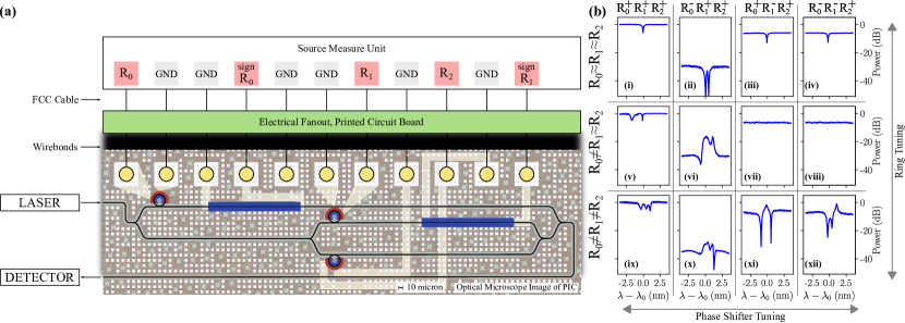
As an initial demonstration, we show the ability of WDIPLN to add and subtract in a simplified form. This represents a fundamental building block of the architecture. While tuning the MRDs ultimately imposes the input/weight onto the circuit, each of the buses in the circuit are additionally reconfigurable via a phase shifter. The phase shifter rotates the phase of a given bus so that we are able to express the sign coefficient of the weights as either or . Bias plays a role in many NN architectures, effectively shifting the set point of the linear fit. Similarly, in this architecture, we can introduce a bias to change our set point. From an optical perspective, this allows us to validate the operation of the circuit via direct measurement through a photodetector at the output [17]. The summation operator occurs as optical interference, which will “add” (constructively interfere) when the phase is the same, and “subtract” (destructively interfere) when the phase is opposite. For an initial demonstration, we consider the optical experiment in Figure 4(a). We designed an WDIPLN circuit with an added bias. There are five active circuit elements: the bias ring, , bias phase shifter, , top arm ring , top arm phase shifter and bottom arm ring . Each element is electrically connected via a wirebond to an electrical fanout, which is in turn wirebonded to a printed circuit board (PCB) and connected to a source measure unit (SMU). The circuit is optically coupled from two single mode fibers (SMF28) embedded in a titled fiber array to two grating couplers on either side of the circuit. A laser and detector pair are connected to the other ends of the respective SMF28 fibers. The MRD we employ is a carrier injection-based PIN micro-ring resonator. We employ a PIN for proof of principle due to the large wavelength change, however, future systems will utilize application specific, optimized MRDs operating in carrier depletion mode. The photonic integrated circuit (PIC) was fabricated in American Institute for Manufacturing (AIM) Photonics’ 300 mm silicon photonics process [28].
We demonstrate a variety of circuit configurations as summarized in Figure 4(b). We achieve these configurations by tuning the phase shifters to or (columns) and setting the rings at various resonant wavelengths (rows), for which we indicate the state of each ring by the label of or . The bias path is slightly shorter than the internal WDILPN, which means we can utilize the phase shifter and the natural wavelength-dependent interference to extract the set-point behavior. Sub-figures (i, v, ix) show three states of addition with phase shifters tuned to where the rings are all aligned to a single resonance (, i), is tuned off (, v), and all the rings are at different resonances (, ix). These states manifest as one, two, or three resonance peaks, respectively. Sub-figures (ii, vi, x) demonstrate the corresponding states where the bias phase is at rather than . Due to manufacturing variations, we observe behavior that deviates from the designed point. In (ii), we expect no signal to pass through; however, due to path and y-branch imbalance, the circuit floor is dB—additionally, small differences in the ring are seen in the transmission. Therefore, the maximum value in (ii) is dB at , where the resonant wavelength sits, which indicates a slight imbalance but overall high suppression of any difference in the rings. Sub-figure (vi) shows two peaks above the minimum, as , and (x) shows three distinguishable peaks as . The peaks are overlapping such that distinguishing individual peaks is difficult. Sub-figures (iii, iv) demonstrate a single resonance, similar to (i); however, note the maximum power is roughly dB since no light passes through in the lower path and each y-branch contributes additional loss of dB. Sub-figures (vii, viii) show detuned , and , where these rings fully cancel out each others’ magnitudes (subtraction). Sub-figures (xi, xii) demonstrate for the subtraction operator, which is seen by the distinct peak difference above and below the bias line. Finally, each flip signs between (xi, xii) due to the phase control of the bias line.
4 Experimental Demonstration of Logic Gates
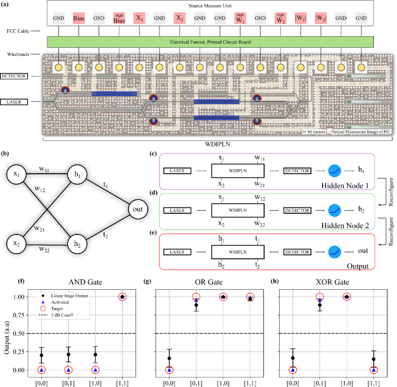
We designed a second circuit in order to demonstrate a learning task. This design reflects the WDIPLN architecture for , as seen in Figure 5(a). This circuit places both input and weight rings along the inner buses, along with a bias branch that also contains a ring. We wirebond out to an electrical carrier, which we then connect to programmable SMU channels in order to electrically control each element. We optically couple the laser and detector through fiber to grating couplers on the input and output waveguides, respectively.
We selected a simple network architecture that is able to reconfigure the weights in order to represent AND, OR and XOR gates, shown in Figure 5(b). We trained these networks on a CPU using PyTorch [31]. For the activation function we employ the rectified linear-unit (ReLU) for all stages. We can create a simple map from the trained model to our physical chip by reconfiguring the chip in between the three linear stages, leading to the three non-input nodes and . For the ring resonators, we define a value of “0” as V and “1” as V. This ensures we are operating in the slightly undercoupled regime for both “0” and “1”. We note that for this demonstration, the and values are globally set for all rings. In addition, the bias ring is set to and the bias phase shifter is set to , specifically for visibility of the full range of through direct detection as opposed to inference [17].
The process of reconfiguration and implementation of the two hidden nodes and the output is shown in Figure 5(c–e). For the two hidden nodes, and , we configure the weights of the optical circuit, namely and , according to the pairs of and , respectively. In addition, if the sign of the weight is negative, we adjust the corresponding phase shifter, namely and from to . Once we configure the chip for , we feed the four input pairs into . For each input, we measure the output from the detector, apply the (ReLU) activation function used in training with a “ dB cutoff”, and record the result. After the two hidden nodes are measured, we reconfigure the circuit for the final stage, according to the final weight stage from training . Finally, we feed the four recorded pairs of into the circuit as inputs, measure the output, apply the activation function and record the result.
According to the training-to-implementation scheme described above and in Figure 5(c–e), we demonstrate the circuit’s performance for three different 2-bit logic gates, namely AND, OR and XOR. In training, the accuracy of this simple network reaches . The resulting outputs of the three gates are shown in Figure 5(f–h). The black dots are the square root (i.e. magnitude) of the output values measured by the detector at the laser probe wavelength, which in this experiment was globally set to nm. The error bars represent the standard output deviation for a pm window around, pm. The blue triangles show the outputs of the circuit after activation, and the red circles show the target for the gates. The AND, OR and XOR gates achieve predictive accuracy of and , respectively.
5 Conclusion
Silicon photonics holds promise for implementing large-scale PNNs directly on chip with substantially improved performance compared to electronic implementations. In this work, we propose and demonstrate a novel PNN architecture, WDIPLN, which exhibits highly favorable characteristics compared to previous literature. The WDIPLN derives from the COLN architecture detailed in [17], enabling similar vector-vector multiplication and summation using an optical carrier signal with the additional benefits of wavelength parallelism, drastically reduced device footprint, and significantly lower energy consumption. The majority of these beneficial properties come from exchanging large, power-hungry MZMs with compact MRDs. While we can trivially exchange the fundamental elements (MRDs for MZMs) in a one-to-one manner to enable multi-channel operation, we show that by replacing the input MRDs with a single, multi-channel MRD with an FSR equal to the weighting channel spacing we can reduce the total device count significantly. As a first proof-of-principle, we experimentally demonstrated simple addition and subtraction between rings in a WDIPLN circuit. We then show a WDIPLN configured with and , which we configure and recycle to perform 2-bit logic gates (AND, OR and XOR). We observe the implementation accuracy for each gate to be and , respectively. Furthermore, the natural wavelength parallelism of the proposed WDIPLN architecture can be exploited using chip-based Kerr frequency comb sources [32] for massive scaling in the frequency domain, similar to recent demonstrations in the silicon photonics platform for high bandwidth data communications [33]. This demonstration opens new opportunities in massively parallel silicon photonic PNNs and paves the way to large-scale systems in the thousand-neuron regime on a single chip with minimal energy consumption.
Data Availability
The data that support the findings of this study are available upon request from the authors.
Appendix A Operating Conditions and Variation of MRDs
The mechanism of tuning for MRDs here is assumed to be electro-optic (where thermo-optic is an accepted simplification) and well defined by free-carrier plasma dispersion [34]. The transfer function from the electrical to optical domain is defined as
| (3) |
where the voltage (V) dependent absorption (or loss) in the cavity lumped with intrinsic cavity loss, is the wavelength- and voltage-dependent phase shift, is the self-coupling coefficient (with a corresponding cross coupling coefficient, , such that ). Equation 3 depicts the coupled effect of tuning, which both changes the loss and the relative cavity size (i.e. phase shift).
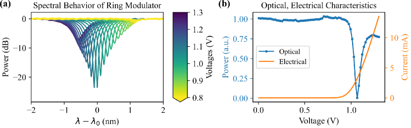
In this work, we employ carrier injection-based ring resonators through the well-known free carrier plasma dispersion effect in silicon. These rings demonstrate a large spectral tuning range, as seen in Figure 6(a). However, this shift comes at the cost of change of coupling conditions due to the strongly voltage-dependent round-trip loss. Changing the coupling conditions from over coupled to critically coupled to under coupled has a large impact on the phase shift associated the ring. It is precisely this phase that we aim to leverage in this architecture. Therefore, we operate the rings in the slightly-to-moderately under coupled regime in this experiment, which corresponds to voltages , as seen in Figure 6(b).
Additionally, this demonstration did not employ thermal tuners to shift the rings coarsely. This leaves the demonstration susceptible to fabrication variations. For large-scale demonstrations, these thermal phase shifters can be implemented with isolated heaters with high efficiency [35, 36] in concert with reverse-biased MRDs for low-power electro-optic configuration [27, 37].
Appendix B Hidden Layer Demonstration Results
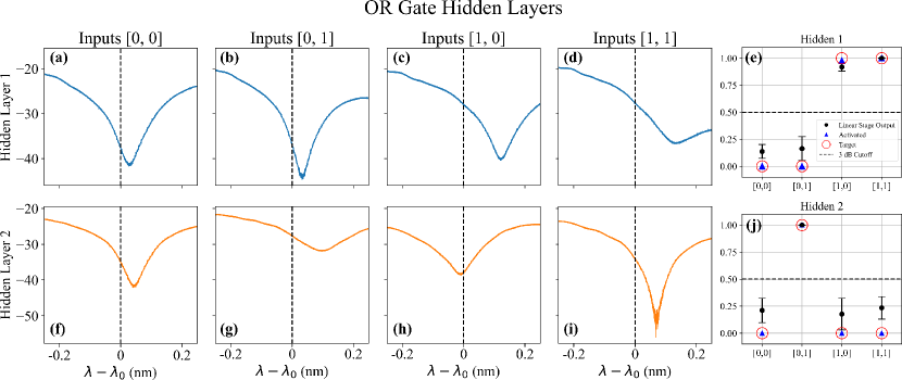
The hidden layers are not explicitly necessary in order to run the network since the final stage weights are known. However, they are important in demonstrating the full generality of the WDIPLN architecture, including the ability to reconfigure. In Figure 7, we show an in-depth look at the procedure of validating the hidden nodes, and . First, we configure the circuit to measure as shown in Figure 5(c). Figure 7(a–d) show the optical circuit response in the Hidden 1 configuration for the four logic inputs, with (e) showing the outputs at the probe wavelength. Figure 7(f–i) shows the optical circuit response in the Hidden 2 configuration for the four logic inputs, with (j) showing the outputs at the probe wavelength.
References
References
- [1] Shen Y, Harris N C, Skirlo S, Prabhu M, Baehr-Jones T, Hochberg M, Sun X, Zhao S, Larochelle H, Englund D et al. 2017 Nature Photonics 11 441–446
- [2] Totović A R, Dabos G, Passalis N, Tefas A and Pleros N 2020 IEEE Journal of Selected Topics in Quantum Electronics 26 1–15
- [3] Shastri B J, Tait A N, Ferreira de Lima T, Pernice W H, Bhaskaran H, Wright C D and Prucnal P R 2021 Nature Photonics 15 102–114
- [4] Nahmias M A, De Lima T F, Tait A N, Peng H T, Shastri B J and Prucnal P R 2019 IEEE Journal of Selected Topics in Quantum Electronics 26 1–18
- [5] Cheng Q, Kwon J, Glick M, Bahadori M, Carloni L P and Bergman K 2020 Proceedings of the IEEE 108 1261–1282
- [6] Nahmias M A, Shastri B J, Tait A N and Prucnal P R 2013 IEEE journal of selected topics in quantum electronics 19 1–12
- [7] Shastri B J, Tait A N, Nahmias M A and Prucnal P R 2014 arXiv preprint arXiv:1407.2917
- [8] Cheng Z, Ríos C, Pernice W H, Wright C D and Bhaskaran H 2017 Science advances 3 e1700160
- [9] Wu C, Yu H, Lee S, Peng R, Takeuchi I and Li M 2021 Nature communications 12 1–8
- [10] Feldmann J, Youngblood N, Karpov M, Gehring H, Li X, Stappers M, Le Gallo M, Fu X, Lukashchuk A, Raja A S et al. 2021 Nature 589 52–58
- [11] Gholipour B, Bastock P, Craig C, Khan K, Hewak D and Soci C 2015 Advanced Optical Materials 3 635–641
- [12] Sun J, Oh S, Choi Y, Seo S, Oh M J, Lee M, Lee W B, Yoo P J, Cho J H and Park J H 2018 Advanced Functional Materials 28 1804397
- [13] Hamerly R, Bernstein L, Sludds A, Soljačić M and Englund D 2019 Physical Review X 9 021032
- [14] Shi B, Calabretta N and Stabile R 2019 IEEE Journal of Selected Topics in Quantum Electronics 26 1–11
- [15] Fouskidis D E, Zoiros K E and Hatziefremidis A 2020 IEEE Journal of Selected Topics in Quantum Electronics 27 1–15
- [16] Zhang H, Gu M, Jiang X, Thompson J, Cai H, Paesani S, Santagati R, Laing A, Zhang Y, Yung M et al. 2021 Nature Communications 12 1–11
- [17] Mourgias-Alexandris G, Totović A, Tsakyridis A, Passalis N, Vyrsokinos K, Tefas A and Pleros N 2019 Journal of Lightwave Technology 38 811–819
- [18] Totovic A, Giamougiannis G, Tsakyridis A, Lazovsky D and Pleros N 2022 Scientific Reports 12 1–13
- [19] Tait A N, Nahmias M A, Shastri B J and Prucnal P R 2014 Journal of Lightwave Technology 32 3427–3439
- [20] Tait A N, De Lima T F, Zhou E, Wu A X, Nahmias M A, Shastri B J and Prucnal P R 2017 Scientific reports 7 1–10
- [21] Williamson I A, Hughes T W, Minkov M, Bartlett B, Pai S and Fan S 2019 IEEE Journal of Selected Topics in Quantum Electronics 26 1–12
- [22] Tait A N, De Lima T F, Nahmias M A, Miller H B, Peng H T, Shastri B J and Prucnal P R 2019 Physical Review Applied 11 064043
- [23] Jha A, Huang C and Prucnal P R 2020 Optics Letters 45 4819–4822
- [24] Mourgias-Alexandris G, Tsakyridis A, Passalis N, Tefas A, Vyrsokinos K and Pleros N 2019 Optics express 27 9620–9630
- [25] Giamougiannis G, Tsakyridis A, Mourgias-Alexandris G, Moralis-Pegios M, Totovic A, Dabos G, Passalis N, Kirtas M, Bamiedakis N, Tefas A et al. 2021 Silicon-integrated coherent neurons with 32gmac/sec/axon compute line-rates using eam-based input and weighting cells 2021 European Conference on Optical Communication (ECOC) (IEEE) pp 1–4
- [26] Mourgias-Alexandris G, Totovic A, Passalis N, Dabos G, Tefas A and Pleros N 2020 Neuromorphic computing through photonic integrated circuits Smart Photonic and Optoelectronic Integrated Circuits XXII vol 11284 (International Society for Optics and Photonics) p 1128403
- [27] Timurdogan E, Sorace-Agaskar C M, Sun J, Shah Hosseini E, Biberman A and Watts M R 2014 Nature communications 5 1–11
- [28] Fahrenkopf N M, McDonough C, Leake G L, Su Z, Timurdogan E and Coolbaugh D D 2019 IEEE Journal of Selected Topics in Quantum Electronics 25 1–6
- [29] Giewont K, Nummy K, Anderson F A, Ayala J, Barwicz T, Bian Y, Dezfulian K K, Gill D M, Houghton T, Hu S, Peng B, Rakowski M, Rauch S, Rosenberg J C, Sahin A, Stobert I and Stricker A 2019 IEEE Journal of Selected Topics in Quantum Electronics 25 1–11
- [30] Littlejohns C G, Rowe D J, Du H, Li K, Zhang W, Cao W, Dominguez Bucio T, Yan X, Banakar M, Tran D et al. 2020 Applied Sciences 10 8201
- [31] Paszke A, Gross S, Massa F, Lerer A et al. 2019 Pytorch: An imperative style, high-performance deep learning library Advances in Neural Information Processing Systems 32 ed Wallach H, Larochelle H, Beygelzimer A, d'Alché-Buc F, Fox E and Garnett R (Curran Associates, Inc.) pp 8024–8035
- [32] Gaeta A L, Lipson M and Kippenberg T J 2019 Nature Photonics 13 158–169
- [33] Rizzo A, Novick A, Gopal V, Kim B Y, Ji X, Daudlin S, Okawachi Y, Cheng Q, Lipson M, Gaeta A L et al. 2021 arXiv preprint arXiv:2109.10297
- [34] Soref R and Bennett B 1987 IEEE journal of quantum electronics 23 123–129
- [35] Coenen D, Oprins H, Ban Y, Ferraro F, Pantouvaki M, Van Campenhout J and De Wolf I 2022 Journal of Lightwave Technology
- [36] van Niekerk M, Deenadalayan V, Rizzo A et al. 2022 Wafer-scale-compatible substrate undercut for ultra-efficient soi thermal phase shifters Submitted and Accepted to CLEO: Science and Innovations (Optical Society of America)
- [37] van Niekerk M, Cheng C et al. 2022 High extinction micro-ring modulator Submitted and Accepted to CLEO: Science and Innovations (Optical Society of America)