Degenerate Distributed Feedback Photonic Structure with Double Grating Exhibiting Degenerate Band Edge
Abstract
We propose a degenerate version of the Bragg condition, associated to a degenerate band edge (DBE). A standard Bragg condition can be implemented using a periodic grating that operates at the regular band edge. The structure we propose to realize a DBE is made of two stacked identical gratings that form two coupled periodic waveguides with broken mirror symmetry. The occurrence of the DBE is verified by using both an eigenmode solver and the calculations of scattering parameters, using full-wave simulations. The proposed structure is a good candidate to conceive a degenerate distributed feedback lasers operating at the DBE.
Index Terms:
Exceptional point of degeneracy; Double grating waveguide; Degenerate band edge laser; Distributed feedback laser.We present a degenerate version of the Bragg condition in a double grating, leading to a 4th order degeneracy, namely a degenerate band edge (DBE), where four eigenmodes coalesce forming a single degenerate eigenmode. Compared to previous studies [1, 2, 3, 4, 5, 6, 7] devoted to the fundamental aspects of the DBE, here we build on those concepts and specifically show a realistic structure that supports a DBE, based on two coupled dielectric layers with periodic gratings, shown in Fig. 1. The standard Bragg condition for a periodic waveguide, where is the Bloch wavenumber, is the waveguide period, and is an integer, is associated with the regular band edge (RBE) [8, 9]. A Bragg condition implies that two modes with power flux in opposite directions merge at a band edge to form a degenerate mode with vanishing group velocity. The Bragg condition is used in distributed feedback (DFB) lasers so that light is reflected in a distributed fashion within a cavity rather than only at the end mirrors [8, 10, 11, 9]. The Bragg condition is implemented through a periodic grating that acts as a dielectric waveguide. DFB lasers require the presence of an active medium in addition to satisfying the Bragg condition to form a self sustained resonant mode that keeps oscillating [9]. The “degenerate DFB” concept presented here could improve laser properties.
The DBE is a particular kind of exceptional point of degeneracy (EPD) of order in a waveguide without loss and gain, where eigenmodes coalesce in their wavenumbers and polarization states. The concept of degeneracy of the eigenvalues and eigenvectors and their perturbation was discussed in [12, 13, 14, 15], and more recently also in [1, 2, 16, 7, 17, 18]. Here, we use those concepts to show that the double grating in Fig. 1 exhibits a DBE (i.e., an EPD of order four) by engineering the structure’s geometrical dimensions. At a DBE the dispersion diagram is locally represented as , where and are the DBE angular frequency and wavenumber, respectively, and the parameter describes the flatness of the dispersion curve. Therefore, because of the very flat dispersion, not only the degenerate mode has a vanishing group velocity , but also its second and third derivatives vanish. Photonic devices operating at the DBE have the potential to exhibit better performance than those operating at the RBE [3, 4, 5, 6, 19, 7, 20, 21].
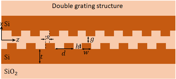
The waveguide with double grating in Fig. 1 consists of a standard grating over a dielectric layer, coupled to another grating obtained by a mirror operation in the direction, followed by a translation along . The shift breaks mirror symmetry, because mirror symmetry prohibits the existence of a DBE in two coupled waveguides due to the existence of even and odd modes that are always decoupled from each other. The double grating in Fig. 1 is made of two silicon on insulator (SOI) waveguides with silicon refractive index , and with a cladding material of silicon dioxide with refractive index .
The modal dispersion relation in Fig. 2 is obtained using the full-wave eigenmode solver implemented in CST Studio Suite. We used periodic boundaries at two virtual cross sections at a distance of a period We look for modes polarized along , hence we use perfect electric conductor (PEC) walls at planes with constant y to account for field invariance in the direction. The computational domain is truncated by PEC also at , where is the dielectric layer thickness as illustrated in Fig. 1, and it is sufficiently large not to affect the field in the grating area, to ensure that the studied modes decay away from the waveguide in the positive and negative directions.
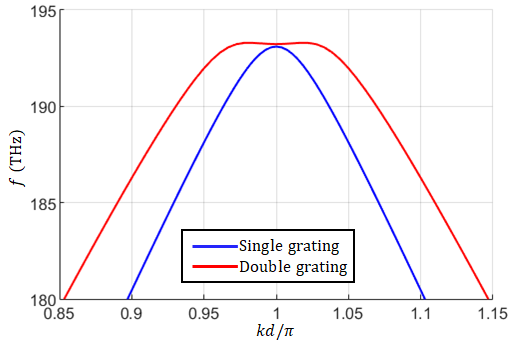
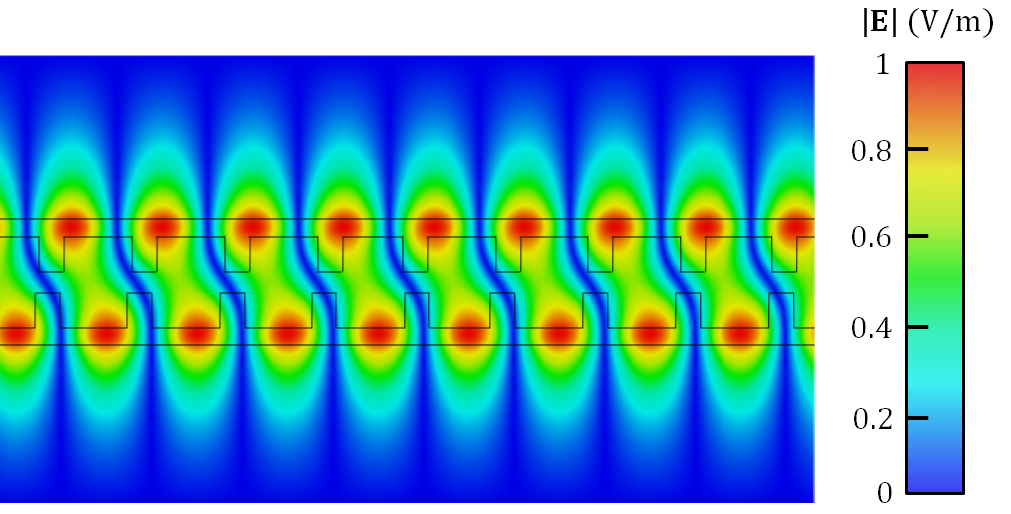
The dielectric waveguide has thickness nm, the gratings has period 335 nm, width nm, and height nm. The rest of parameters, the coupling gap and the shift between the waveguides , are left to be optimized to achieve a DBE. An optimization procedure based on having a DBE in the dispersion relation leads to nm and nm. The dispersion relation obtained from the eignmode solver for the optimized unit cell in the Fig. 1 shows a DBE at around 193 THz (red curve). The flatness of the DBE is compared to that of the the dispersion of modes in the single grating structure (blue curve) with the same waveguide and grating parameters except for the grating height that is now 42 nm in order to have a regular band edge more or less at the DBE frequency of 193 THz. It is clear from the figure that the dispersion relation for the double grating structure (red curve) is flatter than that of single grating structure (blue curve). The field distribution of the DBE mode at is shown in Fig. 1.
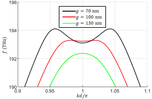
Figure 2 shows the dispersion relation of three distinct designs of the double grating structure in Fig. 1 based on three distinct values of the coupling gap , the rest of the dimensions are the same as the ones mentioned for the case above. Note that for nm the dispersion shows a split band edge [22], with four modes around THz (black curve), which coalesce when using nm. For larger values of , the green curve shows a RBE. Indeed, when a parameter is swept (e.g., ) and one finds both a RBE and a split band edge, there is a proper intermediate value (here, nm) that leads to a DBE [22].
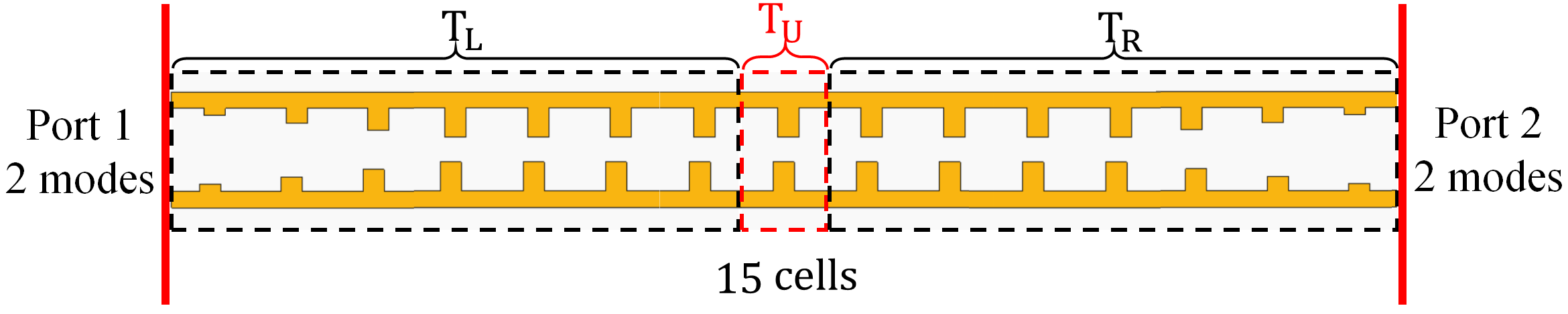
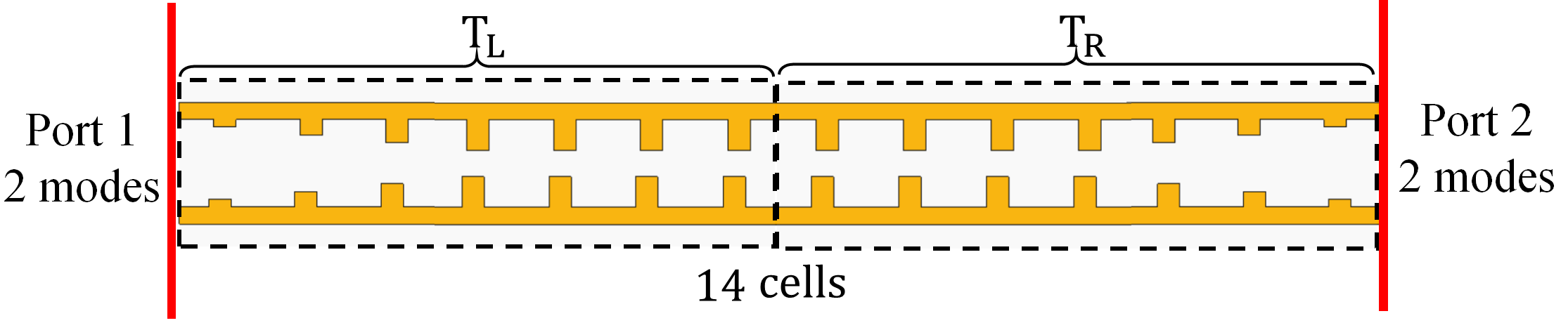
We also verify the existence of the DBE in the proposed double grating structure by finding the scattering matrix using frequency-domain full-wave simulations. Open (radiation) boundaries are used in this simulation and we use waveports as shown in Fig. 3 where two modes (even and odd) are excitable on each port. Note that simulating one unit cell would not lead to an accurate transfer matrix because it would not fully account for the structure periodicity since a waveport supports a waveguide mode and not a Bloch mode. Therefore, in the simulation we include two segments, on the left and right sides of the unit cell, that act as adiabatic transitions between the dielectric waveguide mode and the grating, as shown in Fig. 3. The transition is a chirped grating with height steps of 30 nm, until we reach the whole grating height nm. However our goal is to find the transfer matrix only. Therefore, we also simulated another structure with two chirped gratings as shown in Fig. 3, which is the same structure as in Fig. 3 but without the unit cell at the center. The structure in Fig. 3 is used to deembed the effect of the two transition segments from the results relative to Fig. 3, similarly to what was done in [23, 24].
Using even and odd modes in the ports shown in Fig. 3 and 3, and defining their associated incident and reflected waves
| (1) |
such that . Using full-wave simulations, we find the scattering matrix expressed as
| (2) |
It is convenient to define the state vectors and , relative to port 1 and port 2, respectively. They are defined in way that the first two elements represent the amplitudes of waves propagating in the positive direction, whereas the second two elements represent the amplitudes of waves propagating in the negative direction. As a consequence, the transfer matrix relating them, , is found as [25]
| (3) |
The T-matrices of the two structures shown in Figs. 3 and 3 are and , respectively, where and are the T-matrices of the two chirped grating structures. The chirped structure represented by is a flipped version, in the direction, of the other one represented by , and therefore they satisfy , if is not singular, where is a transformation matrix that flips the direction of wave propagation, made by two in the diagonal blocks and two identity matrices in the codiagonal blocks.
Hence, we calculate the new T-matrix whose eigenvalues are the same of those of the unit-cell T-matrix , similarly to what is done in [23, 24]. The T-matrices and are obtained by transformation of the scattering matrices associated to the 4-port structures in Figs. 3 and Fig. 3 based on3.
According to Floquet-Bloch theory, we look for periodic solutions of the state vector as where is the Floquet-Bloch complex wavenumber, that satisfy , with , where and are the state vectors at the input and output of a unit cell. The eigenvalue problem is then formulated as
| (4) |
where the eigenvalues , with , are obtained by solving the dispersion characteristic equation , with being the identity matrix.
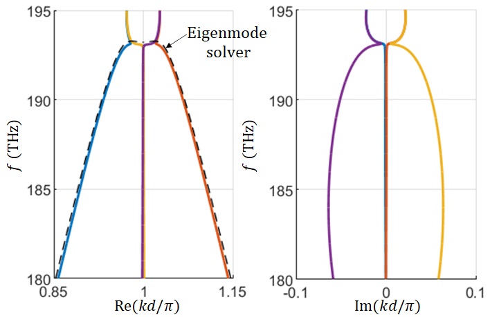
We show in Fig. 3 the Floquet-Bloch complex-valued wavenumber dispersion diagram of the four eigenmodes of the structure in Fig. 1. The dispersion diagram confirms the existence of the DBE at a frequency THz, where four branches coalesce. The black-dashed curve is the dispersion diagram with a purely real wavenumber obtained via the eigenmode solver using phase-shift boundary conditions, shown here for comparison purposes. Indeed, a good matching is found for the curve with purely real wavenumber, which validates the method described above based in the dembedding procedure, that confirms the existence of the DBE.
In conclusion, we have proposed a photonic structure with double grating that exhibits a DBE in its dispersion diagram where a degenerate Bragg condition occurs at . We have demonstrated the occurrence of the DBE using two methods: (i) by finding the dispersion relation of modes with purely real wavenumbers using an eigenmode solver and observing the very flat dispersion, and (ii) by finding the four complex-valued wavenumbers from the scattering parameters by using full-wave simulations. The degenerate Bragg condition we have found in the double grating structure can be used to conceive a “degenerate distributed feedback laser”, that may lead to interesting properties, even augmented when compared to a DFB laser. The first DBE laser analysis was carried out in [19] using a transmission line method for an ideal structure. Interesting properties were found in that ideal DBE structure like stability of the lasing oscillation frequency when varying the load, and lower threshold than the one in the RBE laser, even in the case when the RBE cavity has the same quality factor of the DBE cavity. Future studies shall be devoted to study the cavity effect and the lasing properties of the double grating with degenerate Bragg condition presented in this letter.
Acknowledgment
This material is based on work supported by the Air Force Office of Scientific Research award number FA9550-18-1-0355, and by the National Science Foundation under award NSF ECCS-1711975. The authors are thankful to DS SIMULIA for providing CST Studio Suite that was instrumental in this study.
References
- [1] A. Figotin and I. Vitebskiy, “Gigantic transmission band-edge resonance in periodic stacks of anisotropic layers,” Physical Review E, vol. 72, no. 3, p. 036619, 2005.
- [2] A. Figotin and I. Vitebskiy, “Slow wave phenomena in photonic crystals,” Laser & Photonics Reviews, vol. 5, no. 2, pp. 201–213, 2011.
- [3] A. A. Sukhorukov, C. J. Handmer, C. M. de Sterke, and M. J. Steel, “Slow light with flat or offset band edges in few-mode fiber with two gratings,” Optics Express, vol. 15, no. 26, pp. 17954–17959, 2007.
- [4] N. Gutman, L. C. Botten, A. A. Sukhorukov, and C. M. de Sterke, “Degenerate band edges in optical fiber with multiple grating: efficient coupling to slow light,” Optics Letter, vol. 36, no. 16, pp. 3257–3259, 2011.
- [5] J. R. Burr, N. Gutman, C. M. de Sterke, I. Vitebskiy, and R. M. Reano, “Degenerate band edge resonances in coupled periodic silicon optical waveguides,” Optics Express, vol. 21, no. 7, pp. 8736–8745, 2013.
- [6] M. G. Wood, J. R. Burr, and R. M. Reano, “Degenerate band edge resonances in periodic silicon ridge waveguides,” Optics Letters, vol. 40, no. 11, pp. 2493–2496, 2015.
- [7] M. Y. Nada, M. A. Othman, O. Boyraz, and F. Capolino, “Giant resonance and anomalous quality factor scaling in degenerate band edge coupled resonator optical waveguides,” Journal of Lightwave Technology, vol. 36, no. 14, pp. 3030–3039, 2018.
- [8] H. Kogelnik and C. Shank, “Coupled-wave theory of distributed feedback lasers,” Journal of Applied Physics, vol. 43, no. 5, pp. 2327–2335, 1972.
- [9] H. Ghafouri-Shiraz, Distributed feedback laser diodes and optical tunable filters. John Wiley & Sons: Chichester, England, 2003.
- [10] S. Wang, “Principles of distributed feedback and distributed bragg-reflector lasers,” IEEE Journal of Quantum Electronics, vol. 10, no. 4, pp. 413–427, 1974.
- [11] J. J. Degnan, “The waveguide laser: A review,” Applied physics, vol. 11, no. 1, pp. 1–33, 1976.
- [12] M. I. Vishik and L. A. Lyusternik, “The solution of some perturbation problems for matrices and selfadjoint or non-selfadjoint differential equations i,” Russian Mathematical Surveys, vol. 15, no. 3, pp. 1–73, 1960.
- [13] P. Lancaster, “On eigenvalues of matrices dependent on a parameter,” Numerische Mathematik, vol. 6, no. 1, pp. 377–387, 1964.
- [14] T. Kato, Perturbation Theory for Linear Operators. Springer-Verlag New York Inc., New York, 1966, doi: 10.1007/978-3-662-12678-3.
- [15] A. P. Seyranian, “Sensitivity analysis of multiple eigenvalues,” Journal of Structural Mechanics, vol. 21, pp. 261–284, jan 1993, doi: 10.1080/08905459308905189.
- [16] N. Gutman, C. M. de Sterke, A. A. Sukhorukov, and L. C. Botten, “Slow and frozen light in optical waveguides with multiple gratings: Degenerate band edges and stationary inflection points,” Physical Review A, vol. 85, no. 3, p. 033804, 2012.
- [17] A. F. Abdelshafy, M. A. Othman, D. Oshmarin, A. T. Almutawa, and F. Capolino, “Exceptional points of degeneracy in periodic coupled waveguides and the interplay of gain and radiation loss: Theoretical and experimental demonstration,” IEEE Transactions on Antennas and Propagation, vol. 67, no. 11, pp. 6909–6923, 2019.
- [18] T. Mealy and F. Capolino, “General conditions to realize exceptional points of degeneracy in two uniform coupled transmission lines,” IEEE Transactions on Microwave Theory and Techniques, vol. 68, no. 8, pp. 3342–3354, 2020.
- [19] M. Veysi, M. A. Othman, A. Figotin, and F. Capolino, “Degenerate band edge laser,” Physical Review B, vol. 97, no. 19, p. 195107, 2018.
- [20] A. F. Abdelshafy, D. Oshmarin, M. A. Othman, M. M. Green, and F. Capolino, “Distributed degenerate band edge oscillator,” IEEE Transactions on Antennas and Propagation, vol. 69, no. 3, pp. 1821–1824, 2020.
- [21] D. Oshmarin, A. F. Abdelshafy, A. Nikzamir, M. M. Green, and F. Capolino, “Experimental demonstration of a new oscillator concept based on degenerate band edge in microstrip circuit,” arXiv preprint arXiv:2109.07002, 2021.
- [22] H. Noh, J.-K. Yang, I. Vitebskiy, A. Figotin, and H. Cao, “Giant resonances near the split band edges of two-dimensional photonic crystals,” Physical Review A, vol. 82, no. 1, p. 013801, 2010.
- [23] N. Apaydin, L. Zhang, K. Sertel, and J. L. Volakis, “Experimental validation of frozen modes guided on printed coupled transmission lines,” IEEE transactions on Microwave Theory and Techniques, vol. 60, no. 6, pp. 1513–1519, 2012.
- [24] M. Y. Nada, T. Mealy, and F. Capolino, “Frozen mode in three-way periodic microstrip coupled waveguide,” IEEE Microwave and Wireless Components Letters, vol. 31, no. 3, pp. 229–232, 2020.
- [25] M. Y. Nada, M. A. Othman, and F. Capolino, “Theory of coupled resonator optical waveguides exhibiting high-order exceptional points of degeneracy,” Physical Review B, vol. 96, no. 18, p. 184304, 2017.