Polarizability, plasmons, and screening in 1T′-MoS2 with tilted Dirac bands
Abstract
In the presence of an external vertical electric field and strain, it is evident that 1T′-MoS2 exhibits tilted Dirac bands which are valley-spin-polarized. Additionally, this material experiences a topological phase change between a topological insulator and band insulator for a critical value of the electric field. Using linear response theory, we calculated the polarization function which is in turn employed to obtain the dielectric function. This latter quantity is subsequently utilized in calculations to determine the plasmons dispersion relation, their decay rate and impurity screening corresponding to various levels of doping, the critical applied vertical electric field strengths and the spin-orbit coupling gap in 1T′-MoS2 with tilted Dirac bands.
I Introduction
Massive anisotropic tilted Dirac systems have been gaining an increasing degree of attention among two-dimensional (2D) materials due to their intriguing properties.[1, 2, 3, 4, 5, 6] These include their distinctive anisotropic optical response. [2] Materials like graphene and silicene have an isotropic relativistic spectrum in momentum space. [7, 8] However, it has been found that some of these new materials under consideration have anisotropic linear spectra, namely, tilted anisotropic linear Dirac cones, which is the case for 1T′-MoS2 [1, 2] and 8-Pmmn borophene, [9, 10, 11, 12] partially hydrogenated graphene [13] as well as transition metal dichalcogenides. [2, 14] In effect, the existence of a tilted cone gives rise to fundamentally different electronic and optical behaviors compared with systems whose cones are not tilted. [15] For example, anisotropic plasmon dispersion was reported in Ref. [16] as well as a unique intervalley damping effect. [17, 18]
These materials are semimetals and have no intrinsic band gap, but a gap can be generated by breaking the symmetry, for example. In the case of graphene, the semimetalic behavior can be changed by breaking the inversion symmetry and the opening of a band gap, as demonstrated in Refs. [19, 20], and which leads to the valley Hall effect. It has been found that in the presence of external vertical electric field, 1T′-MoS2 presents valley-spin-polarized tilted Dirac bands. Additionally, for a critical value of the electric field, the system undergoes a topological transition between the topological insulator and band insulator phases. We investigate the effects due to the vertical electric field and doping on the anisotropic polarization function, plasmon excitations and their decay rates as well as impurity screening for tilted Dirac bands for 1T′-MoS2 at T=0 K. These calculations, done using linear response theory, reveal the role played by the combined effect due to spin-orbit coupling, band tilting, and vertical electric field on an important collective property with potential device applications. Our results for 1T′-MoS2 are compared with 8-Pmmn borophene, a polymorph of borophene which has an anisotropic tilted Dirac cone [16], and other monolayer tilted gapped Dirac materials, including SnS2, TaCoTe2, and TaIrTe4, based on the similarity of their band structure.
The rest of this paper is organized as follows. For our theory, we introduce in Sec. II a low-energy model Hamiltonian for 1T′-MoS2. We analytically derive the eigenstates. In Sec. III, we derive the frequency-dependent polarization function and present our numerical results. Section IV is devoted to an investigation of the plasmon excitations and their decay rates for chosen doping and vertical electric field strength. The static shielding of a dilute distribution of impurities is presented in Sec. V. We conclude with a summary in Sec. VI.
II Anisotropic Tilted Dirac Bands Formalism
Within the approximation the low-energy Hamiltonian for a 2D anisotropic tilted Dirac system representing 1T′ -MoS2 in the vicinity of two independent Dirac points located at (0, ) with is given by [2]
| (1) | |||||
In this notation, the 2D wave vector , the spin-orbit coupling parameter eV and the Fermi velocities are given by m/s, m/s, m/s, and m/s. Also, is the unit matrix and we have introduced , , and with, and being unit and Pauli matrices acting in pseudospin space whereas and denote Pauli matrices acting upon real spin space. The normalized electric field is defined via the applied electric field and its critical value .
The energy eigenvalues of Eq. (1) are given by
| (2) |
where for the conduction (valence) band, and is the spin up (down) index. The long wavelength expansion of the energy eigenvalues for applied electric field not close to its critical value, , is
| (3) |
and we see that it depends on both (a linear term) and but only on a quadratic term. Equation (3) also shows that the spin-orbit coupling opens up a gap between spin-subbands and between the valence and conduction bands within a chosen valley. We emphasize that Eq. (3) is not valid in the gapless case.
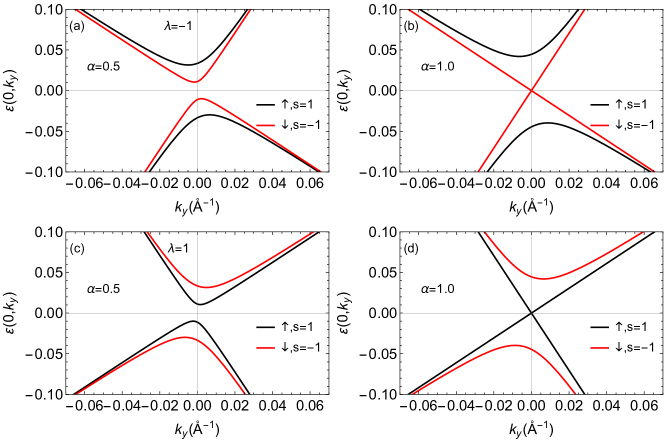
In Fig. 1, we show the spin-polarized bands and the valley-spin polarized gaps in the presence of a vertical electric field (). Notice that an indirect energy gap opens when . The critical points of the energy bands are located at whose coordinate on the -axis for the minima (for ) or maxima (for ) of Eq. (2) are
| (4) |
According to Eq. (4), the critical point is at the origin when which is in agreement with the panels on the right-hand side in Fig. 1 for both spin branches and valleys. We now have an explicit expression for the shifted critical point as well as the tilt by taking the gradient of the expression in Eq. (3).
The wave functions of the Hamiltonian in Eq. (1) are given by the following expression
| (5) |
where is a normalization area and we have introduced .
III Frequency-dependent Polarization function
In the RPA, the polarizability is represented by a particle-hole bubble in the in the Feynman diagram representation. Mathematically, this is for each channel
| (6) |
where is the Fermi-Dirac distribution function under chemical potential and are the energy eigenvalues, can be viewed as an infinitesimal scattering rate. The numerator containing the two statistical functions ensures that the integrand covers only the overlap of particle-hole pairs and (as opposed to particle-particle or hole-hole pairs). The definition of the overlap function is
| (7) |
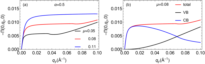
The parameters used in our calculations are the same as before. In Fig. 2, we present the static polarization function versus wave number at zero temperature for various chemical potentials, chosen and . We have included the contributions to the polarizability from both valleys, i.e., . More explicitly, in Figs. 2(a) and 2(b), we set in the sum in Eq. (6) and compare the total value of the polarization function as the chemical potential is varied in Fig. 2(a) whereas Fig. 2(b) shows the individual contributions from the valence (VB) and the conduction (CB) to the total polarizability. These results show that the value of the polarization is increased as the chemical potential is increased but its variation with is not monotonic. Figure 2(b) shows that the contribution to the polarizability is dominated by the conduction band (CB) at longer wavelengths but the valence band (VB) makes the larger contribution as is increased. Our calculations show that the behaviors of the polarizability when are essentially the same as those for in Figs. 2(a) and 2(b). However, we note that at large and high chemical potential, the behavior of the plots is basically linear as it is for monolayer graphene.[21, 22, 23, 24, 25]
IV Anisotropic Plasmon modes
The energy dispersion for the self-sustained plasmon oscillations is determined by the zeros of the dielectric function, , where , with and the plasmon decay rate is
| (8) |
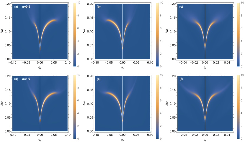
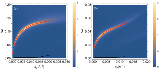
In Fig. 3, we present the plasmon dispersion for whereas in Fig. 4, we present the plasmon dispersion for and . In the former case, the chemical potential crosses both conduction subbands whereas in the latter case, the chemical potential falls just below the minimum of the higher of the two conduction subbands. These results illustrate the anisotropy of the dispersion for both chosen values of , i.e., the plasma frequency depends on the direction of propagation. In all cases, the plasmon modes are Landau damped beyond a critical value of the wave vector which varies with and . As this Landau damping takes place within the particle-hole continuum, we are principally interested in the plasmon branch in the region outside this continuum, where which yields . The presented results also illustrate that the two valleys contribute unequally. Comparing Figs. 3 and 4, we see that the larger has a greater group velocity in the long wavelength limit, thereby accounting for the collective properties of tilted MoS2.
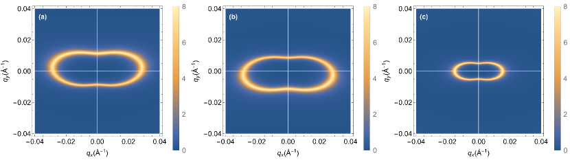
In Fig. 5, we present the plasmon dispersion for where the plasmons isofrequency contours are shown when we sum over both valleys but intervalley terms are not included. Both panels on the left and middle shown in Fig. 5 (a) clearly illustrate the anisotropy of the plasmon dispersion is due to both valleys. Figure 5 demonstrates that the breaking of the symmetry by the electric field leads to a dependence on the direction of propagation of the modes. Choosing a frequency of oscillations in Fig. 5 shows that this value can be achieved in various directions of propagation.
.
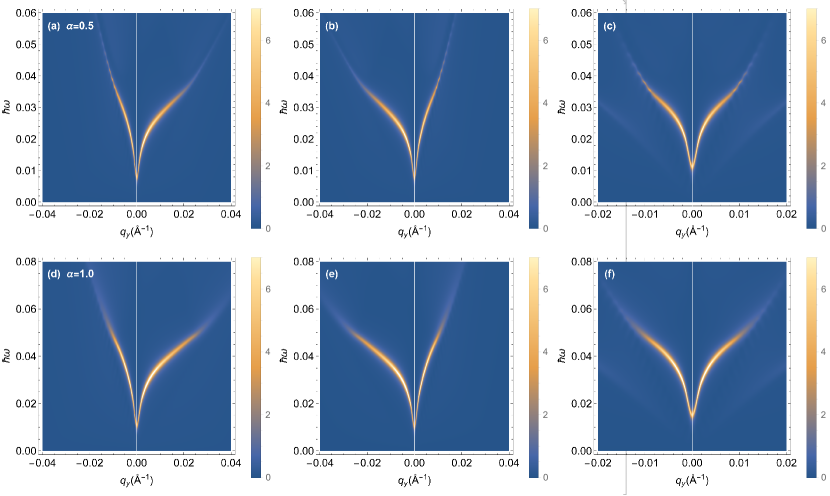
Figure 6 shows the plasmon excitations and corresponding decay rates when and . In Fig. 6(a), the chemical potential is located in the higher conduction subband so that both conduction subbands are partially occupied. However, in Fig. 6(b), the chemical potential is located below the higher conduction subband so that only one conduction sub-bands is partially occupied. The decay rate outside the particle hole region seems enhanced in Fig. 6 shows the plasmon excitations and corresponding decay rates when . In Fig. 6 (a) for the higher chemical potential thereby indicating the tunability of for 1T′-MoS2.
V Static Screening Effects
We now employ the static limit of the polarizability or Lindhard function to calculate the screened Coulomb potential. This means that from the Lindhard function, it is possible to obtain the response of the Dirac fermions in the material to the presence of a magnetic or electric impurity. The potential in the vicinity of a point charge Q is proportional to the Fourier transform of the screened Coulomb interaction
| (9) |
where and since the Lindhard function is anisotropic in -space, we must take into consideration its dependence on the polar angle of integration in Eq. (9).
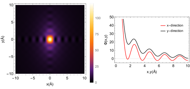
In Fig. 7, we present the static screened potential for a dilute distribution of charge for which Eq. (9) is applicable. The calculated results show evidence of anisotropy along the mutually perpendicular and axes. The screened potential displays Friedel oscillations with directional dependent amplitudes which are phase shifted. This is quite unlike the screened electrostatic potential for graphene and the difference is attributed to the significant variation in their band structures.
VI Concluding Remarks
In conclusion, we have investigated the behavior of the dynamical polarizability, plasmon excitations as well as the static shielding of a dilute distribution of charged impurities for 1T′-MoS2 in the presence of an external vertical electric field and strain. We also demonstrated that the plasmon damping rate generally increases for larger wavevector and larger frequencies along a plasmon branch. Therefore, we expect our damping rate to be monotonically increasing with . The tilted Dirac bands which are valley-spin-polarized cause this material to undergo a topological phase change between a topological insulator and band insulator corresponding to a critical value of the electric field. We employed linear response theory to calculate the polarization function which was obtained numerically at T=0 K. These results were then substituted into the dielectric function for calculating the plasmon dispersion relation, their decay rate and impurity screening. We would like to once again emphasize that here we have calculated both damped and undamped plasmons as zeros of the real part of the dielectric function.
Such distinctive features of 1T′-MoS2 are expected to give rise to a variety of applications which can be used for designing novel multi-functional nanoelectronic and nanoplasmonic devices. Specifically, the control of these collective properties could lead to some important technological applications for electronic and optoelectronic devices.
It is evident that the electron dynamics in1T′-MoS2 under a vertical electric field and strain is significantly different from that in graphene and this variation can be controlled by an electrostatic potential. This further implies that such a difference may be tuned by a structure parameter for 1T′-MoS2. These results presented here are expected to provide very useful information as well as guidance for designing nanoelectronic and nanoplasmonic devices based on innovative low-dimensional 1T′-MoS2 materials
Finally, we observe that the presence of anisotropic plasmons in 1T′-MoS2 like in 8- borophene makes it possible for its use for anisotropic plasma-wave photodetection, in a field-effect transistor–based device.
Acknowledgment(s)
G.G. would like to acknowledge the support from the Air Force Research Laboratory (AFRL) through Grant No. FA9453-21-1-0046
References
- Qian et al. [2014a] X. Qian, J. Liu, L. Fu, and J. Li, Science 346, 1344 (2014a).
- Tan et al. [2021a] C.-Y. Tan, C.-X. Yan, Y.-H. Zhao, H. Guo, H.-R. Chang, et al., Physical Review B 103, 125425 (2021a).
- Mojarro et al. [2021] M. Mojarro, R. Carrillo-Bastos, and J. A. Maytorena, Physical Review B 103, 165415 (2021).
- Ng et al. [2021] R. Ng, A. Wild, M. Portnoi, and R. Hartmann, arXiv preprint arXiv:2111.10760 (2021).
- Tan et al. [2021b] C.-Y. Tan, J.-T. Hou, C.-X. Yan, H. Guo, and H.-R. Chang, arXiv preprint arXiv:2112.09392 (2021b).
- Qi and Zhou [2021] F. Qi and X. Zhou, Chinese Physics B (2021).
- Wehling et al. [2014] T. O. Wehling, A. M. Black-Schaffer, and A. V. Balatsky, Advances in Physics 63, 1 (2014).
- Wang et al. [2015] J. Wang, S. Deng, Z. Liu, and Z. Liu, National Science Review 2, 22 (2015).
- Nakhaee et al. [2018] M. Nakhaee, S. Ketabi, and F. Peeters, Physical Review B 97, 125424 (2018).
- Xu et al. [2016] L.-C. Xu, A. Du, and L. Kou, Physical Chemistry Chemical Physics 18, 27284 (2016).
- Lopez-Bezanilla and Littlewood [2016] A. Lopez-Bezanilla and P. B. Littlewood, Physical Review B 93, 241405 (2016).
- Zhou et al. [2014] X.-F. Zhou, X. Dong, A. R. Oganov, Q. Zhu, Y. Tian, and H.-T. Wang, Physical Review Letters 112, 085502 (2014).
- Lu et al. [2016] H.-Y. Lu, A. S. Cuamba, S.-Y. Lin, L. Hao, R. Wang, H. Li, Y. Zhao, and C. Ting, Physical Review B 94, 195423 (2016).
- Qian et al. [2014b] X. Qian, J. Liu, L. Fu, and J. Li, Science 346, 1344 (2014b).
- Yang et al. [2018] Z.-K. Yang, J.-R. Wang, and G.-Z. Liu, Physical Review B 98, 195123 (2018).
- Sadhukhan and Agarwal [2017] K. Sadhukhan and A. Agarwal, Physical Review B 96, 035410 (2017).
- Islam and Jayannavar [2017] S. F. Islam and A. Jayannavar, Physical Review B 96, 235405 (2017).
- Sári et al. [2014] J. Sári, C. Tőke, and M. O. Goerbig, Physical Review B 90, 155446 (2014).
- Iurov et al. [2019] A. Iurov, G. Gumbs, and D. Huang, Physical Review B 99, 205135 (2019).
- Iurov et al. [2020] A. Iurov, L. Zhemchuzhna, D. Dahal, G. Gumbs, and D. Huang, Physical Review B 101, 035129 (2020).
- Gumbs et al. [2016] G. Gumbs, A. Balassis, D. Dahal, and M. Lawrence Glasser, The European Physical Journal B 89, 1 (2016).
- Roldán et al. [2009] R. Roldán, J.-N. Fuchs, and M. Goerbig, Physical Review B 80, 085408 (2009).
- Roldán et al. [2010] R. Roldán, M. Goerbig, and J. Fuchs, Semiconductor science and technology 25, 034005 (2010).
- Hwang and Sarma [2007] E. Hwang and S. D. Sarma, Physical Review B 75, 205418 (2007).
- Patel et al. [2015] D. K. Patel, S. S. Ashraf, and A. C. Sharma, Physica Status Solidi (b) 252, 1817 (2015).