Intrinsic spin Hall torque in a moiré Chern magnet
In spin torque magnetic memories, electrically actuated spin currents are used to switch a magnetic bit. Typically, these require a multilayer geometry including both a free ferromagnetic layer and a second layer providing spin injection. For example, spin may be injected by a nonmagnetic layer exhibiting a large spin Hall effectHidding and Guimarães (2020); Shao et al. (2021), a phenomenon known as spin-orbit torque. Here, we demonstrate a spin-orbit torque magnetic bit in a single two-dimensional system with intrinsic magnetism and strong Berry curvature. We study AB-stacked MoTe2/WSe2, which hosts a magnetic Chern insulator at a carrier density of one hole per moiré superlattice siteLi et al. (2021). We observe hysteretic switching of the resistivity as a function of applied current. Magnetic imaging using a superconducting quantum interference device reveals that current switches correspond to reversals of individual magnetic domains. The real space pattern of domain reversals aligns precisely with spin accumulation measured near the high-Berry curvature Hubbard band edges. This suggests that intrinsic spin- or valley-Hall torques drive the observed current-driven magnetic switching in both MoTe2/WSe2 and other moiré materialsSharpe et al. (2019); Serlin et al. (2020). The switching current density of is significantly less than reported in other platformsFan et al. (2014); Jiang et al. (2019); Nair et al. (2020) paving the way for efficient control of magnetic order.
To support a magnetic Chern insulator and thus exhibit a quantized anomalous Hall (QAH) effect, a two dimensional electron system must host both spontaneously broken time-reversal symmetry and topologically nontrivial bandsChang et al. (2022). This makes Chern magnets ideal substrates upon which to engineer low-current magnetic switches, because the same Berry curvature responsible for the nontrivial band topology also produces spin- or valley-Hall effects that may be used to effect magnetic switching. Recently, moiré heterostructures emerged as a versatile platform for realizing intrinsic Chern magnetsChen et al. (2020a); Serlin et al. (2020); Polshyn et al. (2020); Li et al. (2021). In these systems, two layers with mismatched lattices are combined, producing a long-wavelength moiré pattern that reconstructs the single particle band structure within a reduced superlattice Brillouin zone. In certain cases, moiré heterostructures host superlattice minibands with narrow bandwidth, placing them in a strongly interacting regime where Coulomb repulsion may lead to one or more broken symmetriesBalents et al. (2020); Andrei et al. (2021). In several such systems, the underlying bands are topologically nontrivialZhang et al. (2019, 2021), setting the stage for the appearance of anomalous Hall effects when combined with time-reversal symmetry breakingSharpe et al. (2019). Notably, in twisted bilayer graphene low current magnetic switching has been observedSharpe et al. (2019); Serlin et al. (2020), though consensus does not exist on the underlying mechanismHe et al. (2020); Su and Lin (2020); Ying et al. (2021).

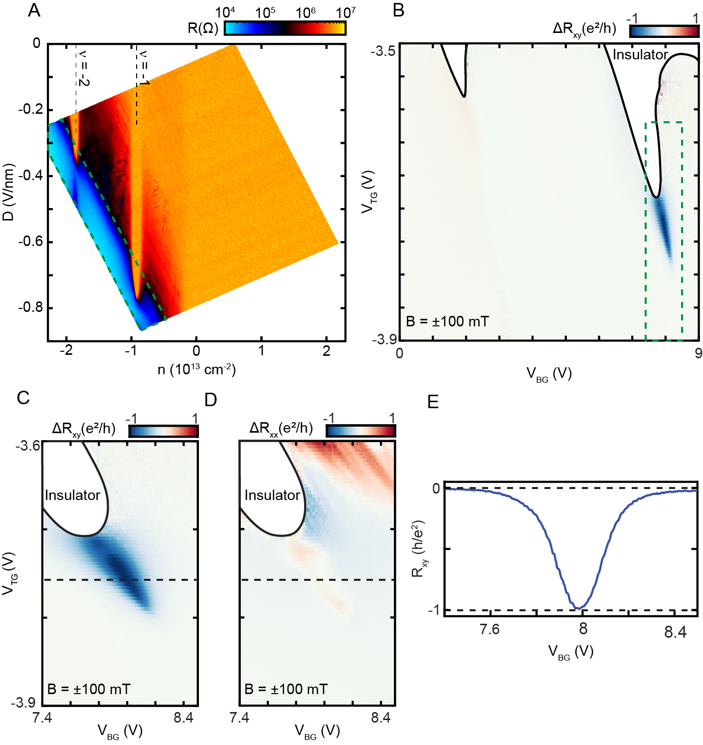
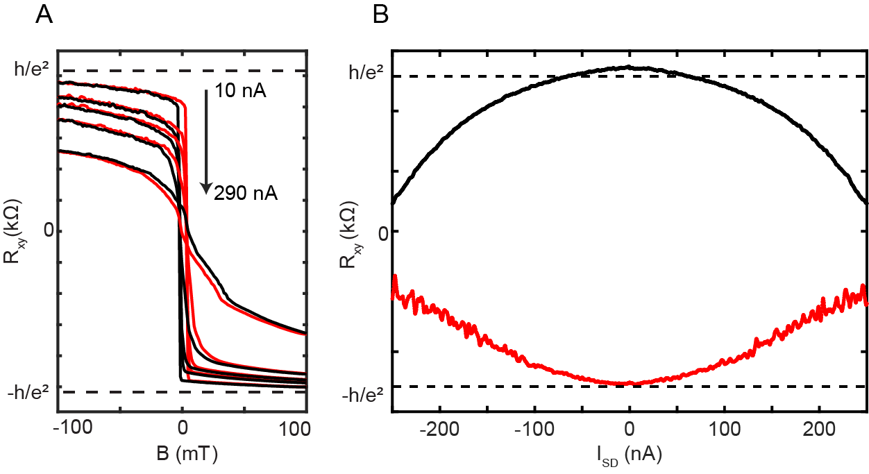
Here, we study a trilayer heterostructure consisting of a MoTe2 bilayer and WSe2 monolayer stacked with 60∘ relative crystal axis alignment (see Methods and Fig. S1), producing a moiré pattern with wavelength nm (Fig. 1a). When subjected to a strong perpendicular electric field, bands from the two semiconducting layers hybridize, producing topologically nontrivial moiré subbandsZhang et al. (2021). At a moiré superlattice filling factor of , corresponding to one hole per superlattice unit cell, we observe a Chern magnet state characterized by a nearly quantized anomalous Hall effect and vanishingly small longitudinal resistance at (Fig. 1b). This is consistent with previous results on AB-stacked MoTe2/WSe2 bilayersLi et al. (2021), where a magnetic Chern insulator arises due to the interplay of strong Coulomb repulsion and underlying Berry curvature of the moiré subbandsPan et al. (2021); Devakul et al. (2021); Xie et al. (2022); Devakul and Fu (2022); Chang and Chang (2022).
Measurements at finite current show hysteretic switching of the resistance in and near the Chern magnet state. Fig. 1c shows the current measured as a function of rising and falling source-drain voltage bias at . We observe hysteretic switching of the current between at least two stable states. The switching current is approximately nA, corresponding to a current density of Acm-2. This is comparable to observations in twisted bilayer grapheneSharpe et al. (2019); Serlin et al. (2020) and significantly less than the lowest observed in spin-orbit torque devicesJiang et al. (2019); Fan et al. (2014). Switching is repeatable, as shown in Fig. 1d.
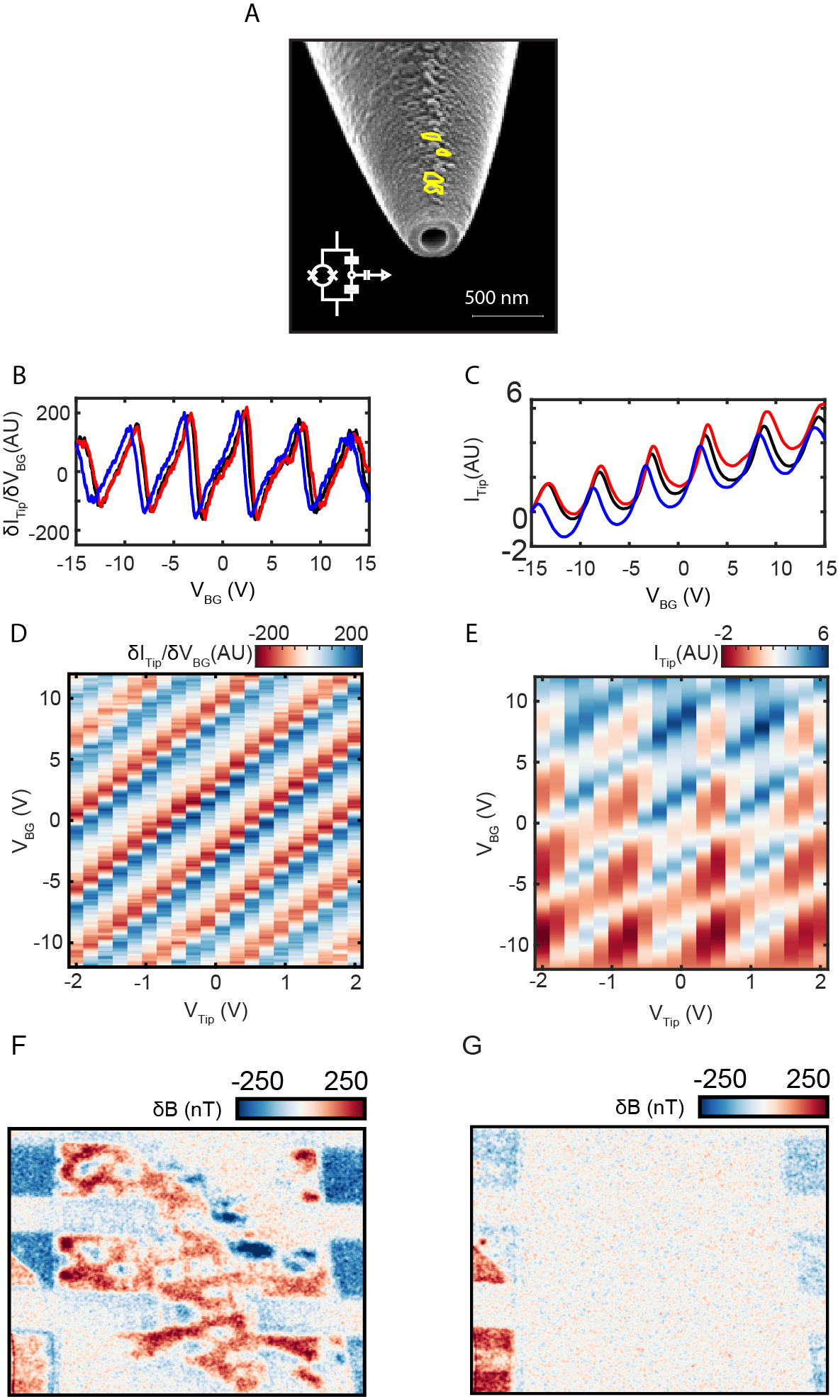
In order to investigate whether the current-driven metastability is related to magnetic domain dynamics, we image the magnetic structure in real space using a nanoscale superconducting quantum interference device (nanoSQUID)Vasyukov et al. (2013); Anahory et al. (2020). The nanoSQUIDs are fabricated from indiumAnahory et al. (2020) on the tip of a cryogenically cooled quartz tube, resulting in sensors with diameters ranging between nm and magnetic field sensitivities 15 nT/Hz1/2. The quartz tube supporting the nanoSQUID is pressed against a piezoelectrically pumped quartz tuning fork, allowing the spatial position of the tip to be modulated in the plane of the sample, providing topographic feedback via shear-force microscopy.
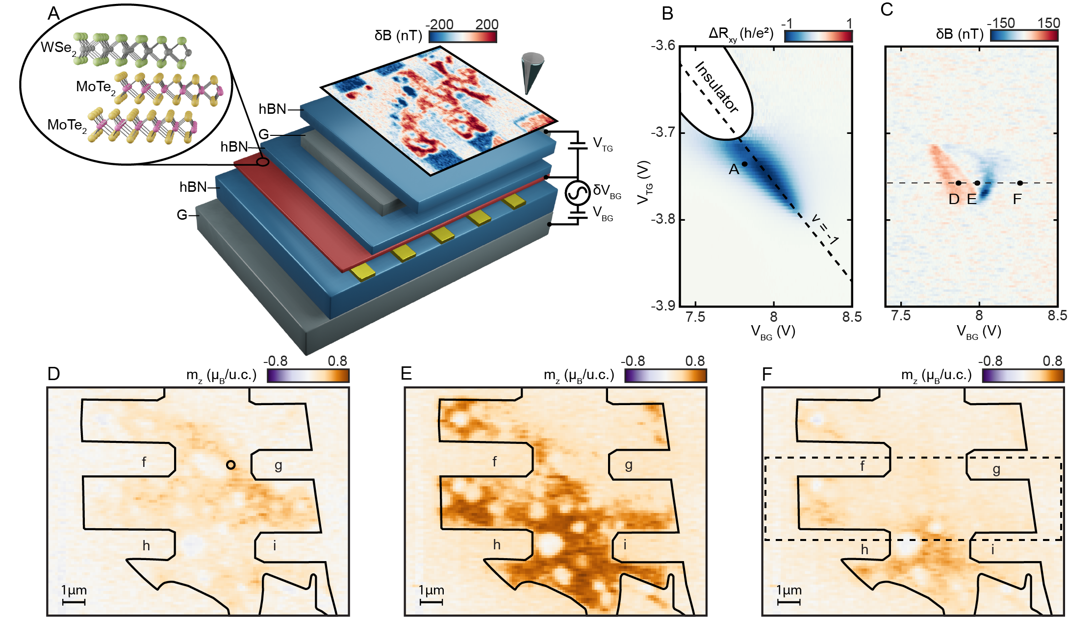
Figure 2a shows a schematic of our measurement geometry. Static voltages are applied to the top gate () and bottom gate () to control the charge carrier density and perpendicular electric displacement field on the grounded MoTe2/WSe2 trilayer (see Supplementary information) In addition, a small AC voltage () is applied to the bottom gate at kHz. Magnetic order, if present, is modulated by , producing a change in the fringe magnetic fields that may be detected by the nanoSQUID at . A real space map of is shown in Fig. 2a, acquired within the regime where the anomalous Hall resistance approaches quantization (see Fig. 2b). Notably, magnetic fields penetrate the graphite top gate without significant modificationbra (1988), allowing us to explore the entire phase diagram tuned by and . In addition, the high electronic compressibility of the graphite screens electrostatic potentials, preventing both unwanted local gating of the sample by the scanning tip and contamination of the magnetic signal by the weak but finite electric-field sensitivity of the nanoSQUID (see Fig. S2).
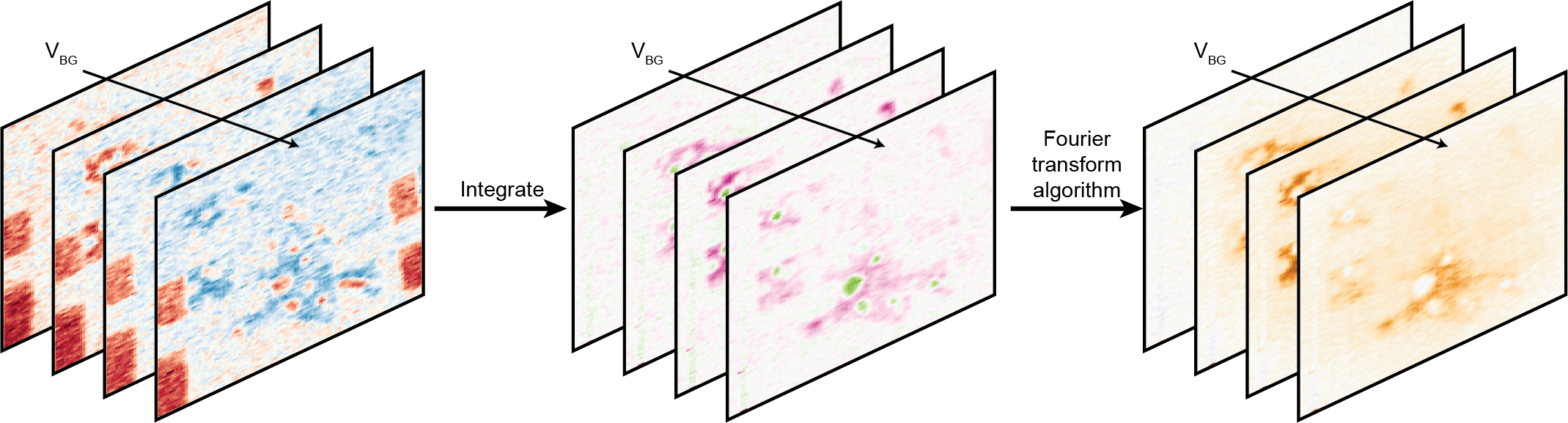
Fig. 2c shows as a function of and measured at a single spatial coordinate. is nonzero in the region of the phase diagram corresponding to the Chern magnet in transport measurements, and vanishes in regions for which . The magnetic field measured above a two dimensional layer is not, in general, a local probe of the magnetization . To extract —which we assume to be oriented in the out-of-plane direction—we first numerically integrate measured over a large real space area along a contour of constant (shown in Fig. 2c). This results in a map of the static , which can then be inverted through a Fourier domain magnetization inversion algorithmTschirhart et al. (2021); Thiel et al. (2019) to obtain (see Fig. S3). Images of for several values of are presented in Fig. 2d-f, and a complete dataset depicting is included in video format in the supplementary data. The active area of the moiré superlattice, defined by the intersection of the graphite top gate, the graphite bottom gate, the MoTe2 bilayer, and the WSe2 monolayer (see Fig. S1), is outlined in solid black line. We find a peak magnetization of The peak coincides with and the QAH effect observed in transport.
The magnetization of the Chern magnet is spatially nonuniform. Throughout the QAH plateau, the bulk of the Chern magnet is riddled with submicron-sized holes. These holes do not become magnetized at any point in () phase space (see Fig. S4) and may correspond to local degradation of the air-sensitive MoTe2 layer, decoupling of the moiré layers, or to the presence of competing structural allotropes of the MoTe2. The presence of these defects does not seem to affect quantization of in the QAH plateau, and the distribution of disorder is robust to thermal cycling (Fig. S5). Inhomogeneity is also evident on much larger, length scales. In particular, the maximal is achieved at different values of in different parts of the device, consistent with long-range variations in the moiré unit cell area. Microscopically, such variations may arise from interlayer strain or variations in the interlayer rotational alignment, though the latter are expected to play a smaller role in the physics of heterobilayers like MoTe2/WSe2 than in homobilayers such as twisted bilayer grapheneLau et al. (2022).

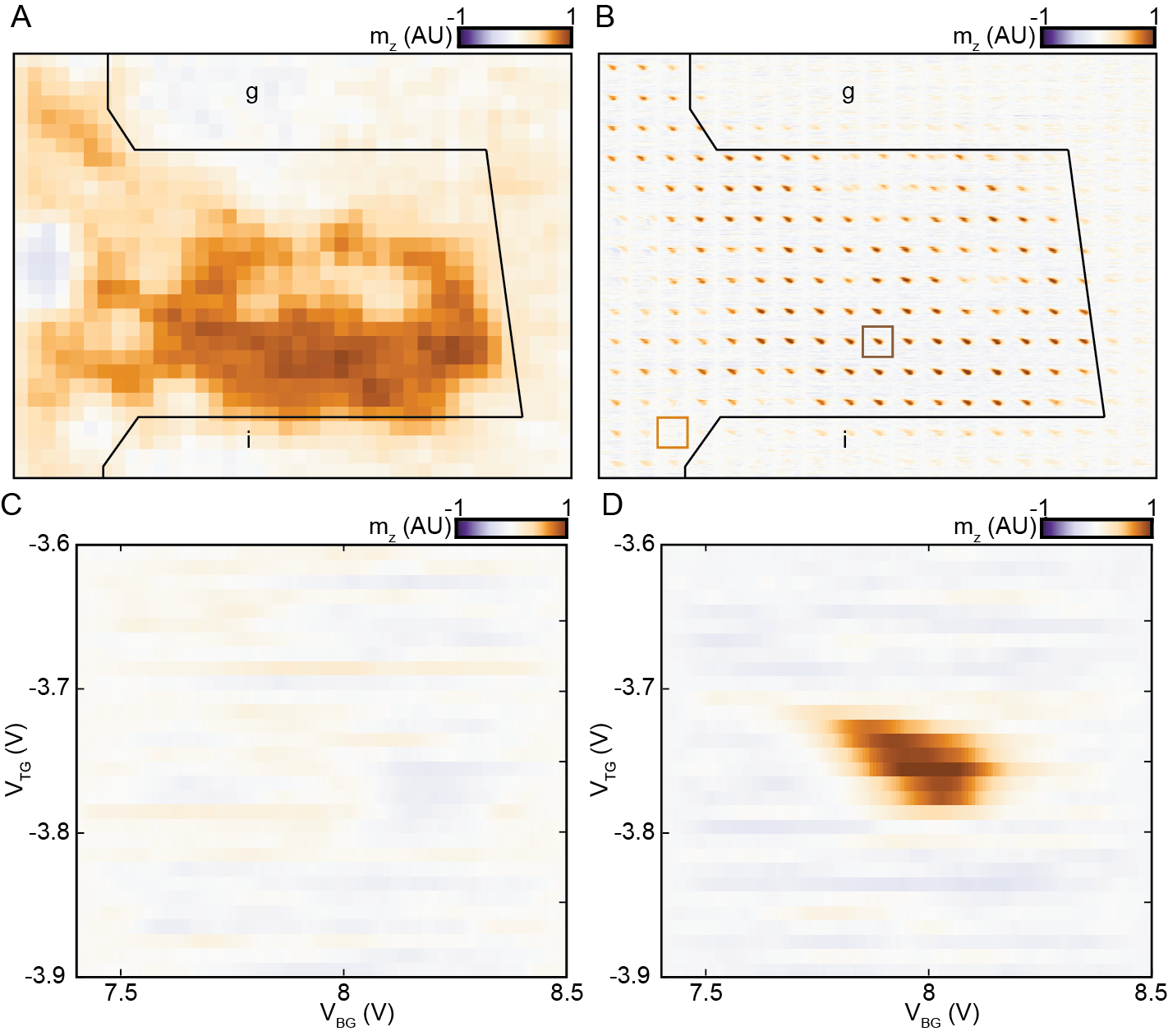
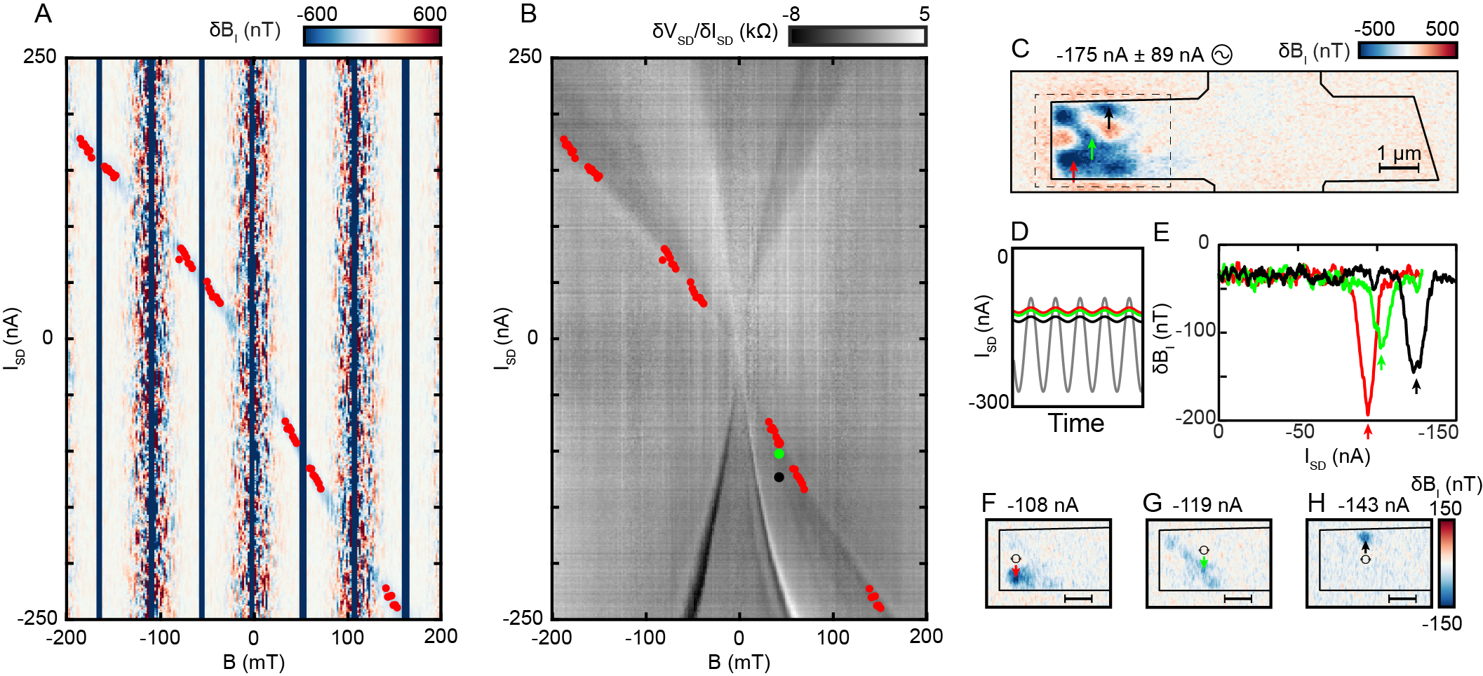
Equipped with a real space map of magnetic order, we may now investigate the origin of the current switching. Figures 3a-b show a detailed dependence of the differential resistance, , on and . As in Fig. 1c, current flows across the entire device, passing from the bottom to the top of the region depicted in Figs. 2d-f. The QAH plateau appears as a local maximum in , and is centered around V. Features associated with current switching appear as sharp dips in differential resistance. Notably switching first occurs at values of where quantization has already begun to degrade (see Fig. S6). We do not observe switching in the quantized regime where current flows only through the chiral edge states, suggesting that bulk current flow is required.
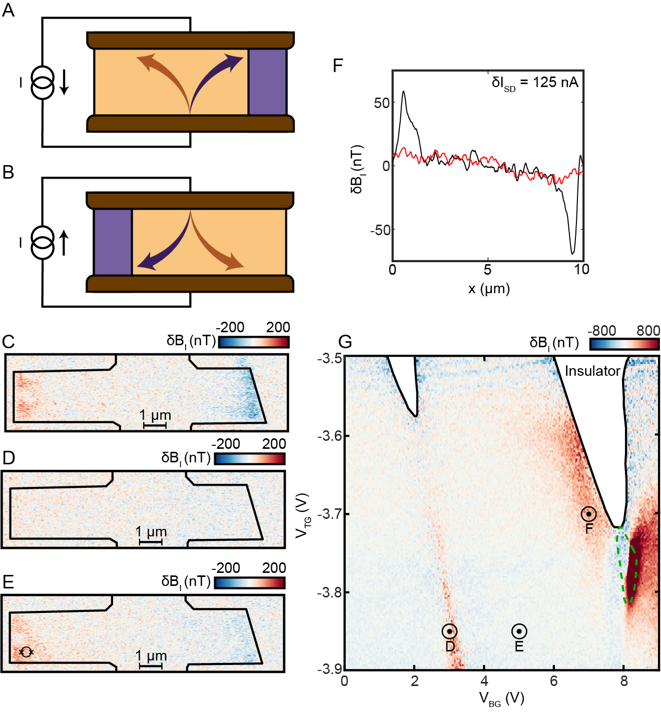
Current switching may be correlated precisely with magnetic structure. Figure 3c shows the change in magnetization relative to the zero current state for nA, well above the threshold current. The image is acquired using tuning fork based gradient magnetometry (see Fig. S7 and Methods) over the scan range depicted by the dashed box in Fig. 2f. Above the threshold, a magnetic domain a few in size is inverted relative to the ground state on one side of the device. Reversing the current flips the side hosting the reversed domain (Fig. 3d). We conclude that the current switching corresponds to the reversal of magnetic domains, with the inverted domains appearing on opposite edges for opposing directions of applied DC current. This is confirmed by the fact that the required switching current increases dramatically as a function of the applied magnetic field (Fig. S8), which increases the energy cost of an inverted magnetic domain.
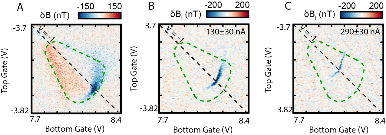
The correspondence between magnetic dynamics and resistivity may be probed in detail by examining the magnetic response, to a small AC current. Figs. 3e and f show , measured near the right and left edges of the device, respectively, for the same range of , , and as Fig. 3a-b. The local signal shows a single sharp dip feature on the right side of the device for and on the left side for , but no signal for the opposite signs (see Fig. S9). These features correlate precisely with the current switching features observed in transport, as evidenced by overlaying a fit to the local dip on the transport data in Fig. 3a-b.
The dips may be understood as a consequence of current-driven domain wall motion. As established above, applied current drives nucleation of minority magnetization domains. Once these domains are nucleated, increasing the current magnitude is expected to enlarge them through domain wall motion. Where domain walls are weakly pinned, a small increase in the current drives a correspondingly small motion of the domain wall, producing a change in the local magnetic field characterized by a sharp negative peak at the domain wall position (Fig. 3g). We may then use this mechanism to map out the microscopic evolution of domains with current. Fig. 3h shows a spatial map of , measured at three different values of corresponding to distinct features in the transport data (see Fig. S8). Evidently, the domain wall moves from its nucleation site on the device boundary towards the device bulk. Local measurements of as a function of show that this motion is itself characterized by threshold behavior, corresponding to the domain wall rapidly moving between stable pinning sites. A full correspondence of transport features and local domain dynamics is presented in Fig. S10.
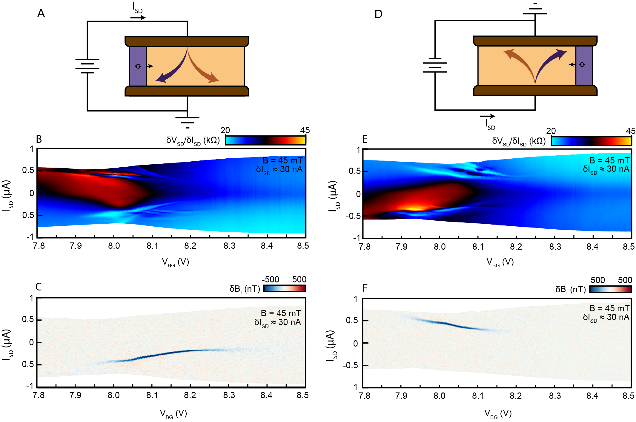
The symmetry of the observed magnetic switching is suggestive of a spin- or valley-Hall effect-driven mechanismShao et al. (2021). In particular, magnetic inversion develops transverse to the applied current, such that the current-induced magnetization gradient, . In this mechanism, depicted schematically in Figs. 4a-b, the current drives opposite spin or valley accumulation on the opposite sides of the device, consistent with our observations of magnetic inversion (Fig. 3c-d). On the edge where the injected moments are not aligned with the equilibrium , they may exert a torque on the ground state magnetic order, reversing it for sufficiently large steady state currents. We refer to this mechanism as intrinsic spin Hall torque; it constitutes an intrinsic, single-layer version of conventional spin-orbit torque where a spin Hall effect layer is used to inject destabilizing moments into a second ferromagnetic layer Shao et al. (2021). The presence of this effect in MoTe2/WSe2 is not surprising, as the same Berry curvature that gives rise to the Chern magnet is expected to generate large spin- and valley- Hall effects, including at non-magnetic and non-integer band fillings.
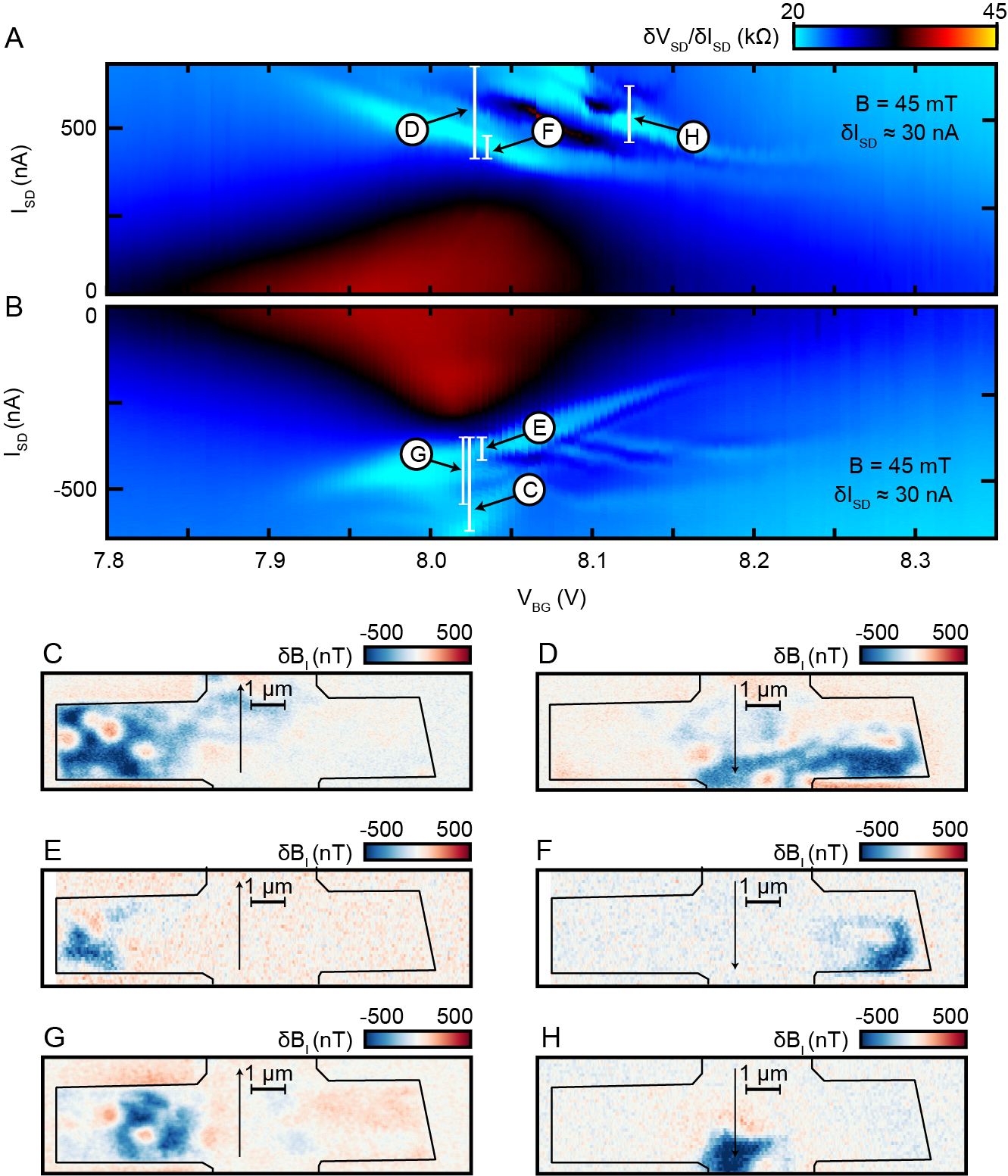
To investigate this hypothesis experimentally, we use local magnetic imaging to directly probe the current-driven accumulation of magnetic moments throughout the density- and displacement field-tuned phase space. Figs. 4c-e show maps measured at three different points, away from the regime where the ground state is ferromagnetic. A magnetic signal consistent with edge magnetic moment accumulationKato et al. (2004) is observed transverse to the applied current near both and , though it is absent for . The accumulation of moments decays into the bulk with a length scale of several microns (Fig. 4f), providing an estimate of the spin diffusion length consistent with measurements of the valley diffusion length in monolayer MoS2Lee et al. (2016). Measurements of at a single point near the edge (Fig. 4g) provide a reasonable proxy for the appearance of a spin- or valley-Hall effect and show that spin Hall-type signals, though ubiquitous, are concentrated in the vicinity of integer fillings and . These fillings correspond to the Hubbard band edges, where the Berry curvature is expected to be enhanced by the appearance of correlation driven gaps, supporting an intrinsic origin for the spin Hall effect.
We have shown here that the combination of intrinsic spin Hall effect with intrinsic magnetism provides a mechanism for a current-actuated magnetic switch in a single two dimensional electron system. The physical properties we invoke to explain this phenomenon are generic to all intrinsic Chern magnets. We emphasize that in both twisted bilayer graphene and our current MoTe2/WSe2 heterostructure, magnetic switching arises in regimes for which doping, elevated temperature, or disorder ensure that electrical current flows in the sample bulk. Ultra-low current switching of magnetic order has been observed in twisted bilayer grapheneSharpe et al. (2019); Serlin et al. (2020); similar physics in that system is presumably governed by orbital, rather than spin, Hall effectsHe et al. (2020). The bulk nature of the spin Hall torque mechanism means that similar phenomena should manifest not only in the growing class of intrinsic Chern magnetsChen et al. (2020b); Polshyn et al. (2020); Deng et al. (2020), but in all metals combining strong Berry curvature and broken time-reversal symmetry, including crystalline graphite multilayersZhou et al. (2021, 2022).
Research into charge-to-spin current transduction has identified a set of specific issues restricting the efficiency of spin torque switching of magnetic orderGupta et al. (2020); Wang et al. (2019). Spin current is not necessarily conserved, and as a result a wide variety of spin current sinks exist within typical spin torque devices. Extensive evidence indicates that in many spin torque systems a significant fraction of the spin current is destroyed or reflected at the spin-orbit material/magnet boundarySchmidt et al. (2000). In addition, the transition metals used as magnetic bits in traditional spin-orbit torque devices are electrically quite conductive, and can thus shunt current around the spin-orbit material, preventing it from generating spin current.
These issues are entirely circumvented here through the use of a material that combines a spin Hall effect with magnetism, and as a result of these effects this spin Hall torque device has better current-switching efficiency than any known spin torque device.
I Acknowledgements
The authors acknowledge discussions with A. Macdonald, D. Ralph, Kelly Luo, Vishakha Gupta, Rakshit Jain, Nai Chao Hu, Bowen Shen, and Zui Tao. Work at UCSB was primarily supported by the Army Research Office under award W911NF-20-2-0166 and by the Gordon and Betty Moore Foundation EPIQS program under award GBMF9471. Work at Cornell was funded by the Air Force Office of Scientific Research under award no. FA9550-19-1-0390. K.W. and T.T. acknowledge support from JSPS KAKENHI (Grant Numbers 19H05790, 20H00354 and 21H05233). ER and TA were supported by the National Science Foundation through Enabling Quantum Leap: Convergent Accelerated Discovery Foundries for Quantum Materials Science, Engineering and Information (Q-AMASE-i) award number DMR-1906325. CLT acknowledges support from the Hertz Foundation and from the National Science Foundation Graduate Research Fellowship Program under grant 1650114.
II Methods
II.1 Device fabrication
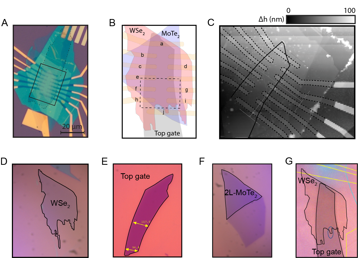
AB-stacked 2L-MoTe2/WSe2 devices were fabricated using the layer-by-layer dry transfer method discussed in detail in Li et al. (2021). An optical image of the device is presented in Fig. S1a. A dashed line identifies the extent of the few-layer graphene bottom gate. A black rectangle identifies a region illustrated in schematic form in Fig. S1b. Contact is made to the moiré superlattice formed by the MoTe2 and WSe2 crystals with nm platinum contacts prepatterned onto a hBN flake; these are themselves contacted with gold wires outside the encapsulated region of the heterostructure. The contacts used for the measurements presented here are labelled in Fig. S1b and are referred to throughout the main text using these labels. Contacts f, g, h, and i are used to probe and in the Chern magnet. The relative locations of the WSe2 monolayer, MoTe2 bilayer, and few-layer graphene top gate are marked in red, blue, and light gray, respectively. The region of overlap between these three flakes defines the device- the bottom gate is omitted for simplicity; it covers this region of overlap entirely, and thus does not define any edges of the dual-gated moiré superlattice. A dashed rectangle identifies the region imaged using nanoSQUID magnetometry in Fig. 2. The precise locations of the contacts relative to the device were determined using atomic force microscopy (AFM); this data is presented with an overlaid outline of the top gate (black line) and contacts (dashed lines) in S1c.
Optical images of the WSe2 monolayer, the few-layer graphene top gate, and the MoTe2 bilayer are presented in Fig. S1d-f. The crystal axes of the MoTe2 and WSe2 flakes were identified optically using angle-resolved second harmonic generation (SHG) and aligned with a 60∘ offset. In the case of the MoTe2 bilayer (for which SHG cannot provide useful information) the crystal axes were identified for an attached monolayer (Fig. S1f). The relative positions of the top gate and WSe2 flake were determined using optical microscopy during the stacking process (Fig. S1g).
II.2 Electrical transport measurements
The measurements presented here were conducted in a pumped liquid helium cryostat at a base temperature of 1.6K. AC transport data was acquired using a finite frequency excitation pA at Hz for Fig. 1b and 2b and kHz for Fig. 3a-b. Data in Figs. 1b and 2 b are field symmetrized, so the plotted resistivity R = and R = .
II.3 Magnetic imaging
Magnetic imaging is performed using a nanoscale superconducting quantum interference device (nanoSQUID). The typical static magnetic field in the region of space accessible by the nanoSQUID is below the DC noise floor of our sensor. Therefore, it is necessary to generate signals at finite frequency. We employ several different methods to generate the data presented in the main text and extended data figures including bottom gate modulation, spatial modulation of the nanoSQUID position, and modulation of the current in the device. Additional descriptions of these several techniques used to generate the data in the main text are available in the literatureVasyukov et al. (2017); Anahory et al. (2020); Uri et al. (2020); Tschirhart et al. (2021).
II.3.1 Bottom gate modulation magnetometry
As discussed in the main text, the magnetic signal may be modulated via carrier density variation, producing an AC response in the local magnetic field detected by the nanoSQUID. In practice, this is implemented using the circuit shown in Fig. 2a. For the data shown in Figs. 2a, c, d-e, Fig. S3, the bottom gate modulation has peak-peak amplitude of mV applied at frequency kHz. We assume the resulting spatial map of obeys .
We reconstruct the magnetization under the assumption that it is entirely out-of-plane, so that . Reconstructed is shown in Figs. 2d-e, S3, and S4. To do this, we first determine , which is accomplished by acquiring over a continuous range of that spans the entire range of the magnetism. As described in Fig. S2, the nanoSQUID is also sensitive to electric fields due to parasitic conduction through quantum dots near the tip. However, the dependence of this signal is screened by the top gate, and varies slowly with in the device regions outside the extent of the top gate. This spurious signal is eliminated by assuming that for values of both lower and higher than the narrow domain of where we observe magnetic structure in the bulk and in transport. Reconstruction of the magnetization from may then be done by Fourier transform techniques identical to those described in Tschirhart et al. (2021). A schematic of this analysis is shown in Fig. S3, and video format data of the bottom gate evolution are available as supplementary data.
II.3.2 Spatial gradient magnetometry
Figs. 3c-d show a reconstruction of the steady state magnetization under an applied DC current. To avoid convolving modulations of the resistivity by the bottom gate with our detected SQUID signal, the magnetization is measured using gradient magnetometry. In this technique, we contact the nanoSQUID tip with a piezoelectric tuning fork (TF) which is modulated at kHz. The resulting modulation of the in-plane nanoSQUID tip displacement produces a signal , where is the vector describing the spatial modulation of the tip. As described in both Tschirhart et al. (2021) and Fig. S7, tuning fork measurements produce a number of additional spurious signals arising from electric fields and mechanical interactions with the surface. However, as in the bottom gate modulation magnetometry, these do not vary with the independent variable of interest here, the applied DC current . We thus analyze the difference images between zero and finite DC current, which contain only . To convert to , we integrate the signal along the direction of the oscillation, producing a map of . This may then be converted to using the same standard Fourier domain analysis techniques described above and in Tschirhart et al. (2021). We did not precisely calibrate during this experimental run, and so provide the extracted in arbitrary units. However, prior work with the identical setupTschirhart et al. (2021) allows us to estimate both the magnitude nm and direction of (see Fig. S7i).
II.3.3 Current modulation magnetometry
As described in the main text, AC currents may also modulate magnetic structure and thus the local magnetic field signal. Data in Figs. 3e,f,h,i, 4c-g, S8a,c,e-h, S9e-f, S10b-g, are all acquired in this way, with a current modulation applied at kHz. The contact configuration and amplitude of the applied current vary between data sets. Applying AC and DC bias to the source contact and grounding the drain, the parameters are:
-
•
Source=j ; Drain=a,b,c,d
nA
-
•
Source=a,b,c,d ; Drain=j
nA
-
•
Source=a,b,c,d ; Drain=j
nA
-
•
Fig. S8a
Source=a,b,c,d ; Drain=j
nA
-
•
Fig. S8c
Source=a,b,c,d ; Drain=j
nA
-
•
Fig. 4c-f
Source= j; Drain=a,b,c,d
nA
-
•
Fig. 4g
Source= j; Drain=a,b,c,d
nA
-
•
Fig. S10b,d,f
Source= a,b,c,d; Drain=j
indicated on figure.
-
•
Fig. S10b,d,f
Source= j; Drain=a,b,c,d
indicated on figure.
Throughout the main text figures, we standardize the phase of the AC current such that positive corresponds to increasing magnitude of current.
References
- Hidding and Guimarães (2020) J. Hidding and M. H. D. Guimarães, Frontiers in Materials 7 (2020).
- Shao et al. (2021) Q. Shao, P. Li, L. Liu, H. Yang, S. Fukami, A. Razavi, H. Wu, K. Wang, F. Freimuth, Y. Mokrousov, M. D. Stiles, S. Emori, A. Hoffmann, J. Åkerman, K. Roy, J.-P. Wang, S.-H. Yang, K. Garello, and W. Zhang, IEEE Transactions on Magnetics 57, 1 (2021), conference Name: IEEE Transactions on Magnetics.
- Li et al. (2021) T. Li, S. Jiang, B. Shen, Y. Zhang, L. Li, Z. Tao, T. Devakul, K. Watanabe, T. Taniguchi, L. Fu, J. Shan, and K. F. Mak, Nature 600, 641 (2021), number: 7890 Publisher: Nature Publishing Group.
- Sharpe et al. (2019) A. L. Sharpe, E. J. Fox, A. W. Barnard, J. Finney, K. Watanabe, T. Taniguchi, M. A. Kastner, and D. Goldhaber-Gordon, Science 365, 605 (2019).
- Serlin et al. (2020) M. Serlin, C. L. Tschirhart, H. Polshyn, Y. Zhang, J. Zhu, K. Watanabe, T. Taniguchi, L. Balents, and A. F. Young, Science 367, 900 (2020), publisher: American Association for the Advancement of Science Section: Report.
- Fan et al. (2014) Y. Fan, P. Upadhyaya, X. Kou, M. Lang, S. Takei, Z. Wang, J. Tang, L. He, L.-T. Chang, M. Montazeri, G. Yu, W. Jiang, T. Nie, R. N. Schwartz, Y. Tserkovnyak, and K. L. Wang, Nature Materials 13, 699 (2014).
- Jiang et al. (2019) M. Jiang, H. Asahara, S. Sato, T. Kanaki, H. Yamasaki, S. Ohya, and M. Tanaka, Nature Communications 10, 2590 (2019).
- Nair et al. (2020) N. L. Nair, E. Maniv, C. John, S. Doyle, J. Orenstein, and J. G. Analytis, Nature Materials 19, 153 (2020), number: 2 Publisher: Nature Publishing Group.
- Chang et al. (2022) C.-Z. Chang, C.-X. Liu, and A. H. MacDonald, arXiv:2202.13902 [cond-mat] (2022), arXiv: 2202.13902.
- Chen et al. (2020a) G. Chen, A. L. Sharpe, E. J. Fox, S. Wang, B. Lyu, L. Jiang, H. Li, K. Watanabe, T. Taniguchi, M. F. Crommie, M. A. Kastner, Z. Shi, D. Goldhaber-Gordon, Y. Zhang, and F. Wang, arXiv:2012.10075 [cond-mat] (2020a), arXiv: 2012.10075.
- Polshyn et al. (2020) H. Polshyn, J. Zhu, M. A. Kumar, Y. Zhang, F. Yang, C. L. Tschirhart, M. Serlin, K. Watanabe, T. Taniguchi, A. H. MacDonald, and A. F. Young, Nature 588, 66 (2020).
- Balents et al. (2020) L. Balents, C. R. Dean, D. K. Efetov, and A. F. Young, Nature Physics 16, 725 (2020).
- Andrei et al. (2021) E. Y. Andrei, D. K. Efetov, P. Jarillo-Herrero, A. H. MacDonald, K. F. Mak, T. Senthil, E. Tutuc, A. Yazdani, and A. F. Young, Nature Reviews Materials , 1 (2021), publisher: Nature Publishing Group.
- Zhang et al. (2019) Y.-H. Zhang, D. Mao, Y. Cao, P. Jarillo-Herrero, and T. Senthil, Physical Review B 99, 075127 (2019).
- Zhang et al. (2021) Y. Zhang, T. Devakul, and L. Fu, Proceedings of the National Academy of Sciences 118 (2021), 10.1073/pnas.2112673118, publisher: National Academy of Sciences Section: Physical Sciences.
- He et al. (2020) W.-Y. He, D. Goldhaber-Gordon, and K. T. Law, Nature Communications 11, 1650 (2020), number: 1 Publisher: Nature Publishing Group.
- Su and Lin (2020) Y. Su and S.-Z. Lin, Physical Review Letters 125, 226401 (2020), publisher: APS.
- Ying et al. (2021) X. Ying, M. Ye, and L. Balents, Physical Review B 103, 115436 (2021), publisher: APS.
- Pan et al. (2021) H. Pan, M. Xie, F. Wu, and S. D. Sarma, arXiv:2111.01152 [cond-mat] (2021), arXiv: 2111.01152.
- Devakul et al. (2021) T. Devakul, V. Crépel, Y. Zhang, and L. Fu, Nature Communications 12, 6730 (2021), number: 1 Publisher: Nature Publishing Group.
- Xie et al. (2022) Y.-M. Xie, C.-P. Zhang, J.-X. Hu, K. F. Mak, and K. Law, Physical Review Letters 128, 026402 (2022), publisher: American Physical Society.
- Devakul and Fu (2022) T. Devakul and L. Fu, arXiv:2109.13909 [cond-mat] (2022), arXiv: 2109.13909.
- Chang and Chang (2022) Y.-W. Chang and Y.-C. Chang, arXiv:2203.10088 [cond-mat] (2022), arXiv: 2203.10088.
- Vasyukov et al. (2013) D. Vasyukov, Y. Anahory, L. Embon, D. Halbertal, J. Cuppens, L. Neeman, A. Finkler, Y. Segev, Y. Myasoedov, M. L. Rappaport, M. E. Huber, and E. Zeldov, Nature Nanotechnology 8, 639 (2013).
- Anahory et al. (2020) Y. Anahory, H. R. Naren, E. O. Lachman, S. B. Sinai, A. Uri, L. Embon, E. Yaakobi, Y. Myasoedov, M. E. Huber, R. Klajn, and E. Zeldov, Nanoscale 12, 3174 (2020), publisher: The Royal Society of Chemistry.
- bra (1988) in Modern Problems in Condensed Matter Sciences, Semimetals, Vol. 20, edited by N. B. Brandt, S. M. Chudinov, and Y. G. Ponomarev (Elsevier, 1988) pp. 175–196.
- Tschirhart et al. (2021) C. L. Tschirhart, M. Serlin, H. Polshyn, A. Shragai, Z. Xia, J. Zhu, Y. Zhang, K. Watanabe, T. Taniguchi, M. E. Huber, and A. F. Young, Science (2021), 10.1126/science.abd3190, publisher: American Association for the Advancement of Science Section: Report.
- Thiel et al. (2019) L. Thiel, Z. Wang, M. A. Tschudin, D. Rohner, I. Gutiérrez-Lezama, N. Ubrig, M. Gibertini, E. Giannini, A. F. Morpurgo, and P. Maletinsky, Science 364, 973 (2019).
- Lau et al. (2022) C. N. Lau, M. W. Bockrath, K. F. Mak, and F. Zhang, Nature 602, 41 (2022), number: 7895 Publisher: Nature Publishing Group.
- Kato et al. (2004) Y. K. Kato, R. C. Myers, A. C. Gossard, and D. D. Awschalom, Science 306, 1910 (2004).
- Lee et al. (2016) J. Lee, K. F. Mak, and J. Shan, Nature Nanotechnology 11, 421 (2016), number: 5 Publisher: Nature Publishing Group.
- Chen et al. (2020b) G. Chen, A. L. Sharpe, E. J. Fox, Y.-H. Zhang, S. Wang, L. Jiang, B. Lyu, H. Li, K. Watanabe, T. Taniguchi, Z. Shi, T. Senthil, D. Goldhaber-Gordon, Y. Zhang, and F. Wang, Nature 579, 56 (2020b), number: 7797 Publisher: Nature Publishing Group.
- Deng et al. (2020) Y. Deng, Y. Yu, M. Z. Shi, Z. Guo, Z. Xu, J. Wang, X. H. Chen, and Y. Zhang, Science (2020), 10.1126/science.aax8156.
- Zhou et al. (2021) H. Zhou, T. Xie, A. Ghazaryan, T. Holder, J. R. Ehrets, E. M. Spanton, T. Taniguchi, K. Watanabe, E. Berg, M. Serbyn, and A. F. Young, Nature 598, 429 (2021).
- Zhou et al. (2022) H. Zhou, L. Holleis, Y. Saito, L. Cohen, W. Huynh, C. L. Patterson, F. Yang, T. Taniguchi, K. Watanabe, and A. F. Young, Science 375, 774 (2022), publisher: American Association for the Advancement of Science.
- Gupta et al. (2020) V. Gupta, T. M. Cham, G. M. Stiehl, A. Bose, J. A. Mittelstaedt, K. Kang, S. Jiang, K. F. Mak, J. Shan, R. A. Buhrman, and D. C. Ralph, Nano Letters 20, 7482 (2020), publisher: American Chemical Society.
- Wang et al. (2019) X. Wang, J. Tang, X. Xia, C. He, J. Zhang, Y. Liu, C. Wan, C. Fang, C. Guo, W. Yang, Y. Guang, X. Zhang, H. Xu, J. Wei, M. Liao, X. Lu, J. Feng, X. Li, Y. Peng, H. Wei, R. Yang, D. Shi, X. Zhang, Z. Han, Z. Zhang, G. Zhang, G. Yu, and X. Han, Science Advances 5, eaaw8904 (2019), publisher: American Association for the Advancement of Science Section: Research Article.
- Schmidt et al. (2000) G. Schmidt, D. Ferrand, L. W. Molenkamp, A. T. Filip, and B. J. van Wees, Physical Review B 62, R4790 (2000), publisher: American Physical Society.
- Vasyukov et al. (2017) D. Vasyukov, L. Ceccarelli, M. Wyss, B. Gross, A. Schwarb, A. Mehlin, N. Rossi, G. Tütüncüoglu, F. Heimbach, R. R. Zamani, A. Kovács, A. F. i. Morral, D. Grundler, and M. Poggio, arXiv:1709.09652 [cond-mat] (2017), arXiv: 1709.09652.
- Uri et al. (2020) A. Uri, Y. Kim, K. Bagani, C. K. Lewandowski, S. Grover, N. Auerbach, E. O. Lachman, Y. Myasoedov, T. Taniguchi, K. Watanabe, J. Smet, and E. Zeldov, Nature Physics 16, 164 (2020), number: 2 Publisher: Nature Publishing Group.
III Extended data figures


IV Supplementary materials