A simple strategy to measure the contact resistance between metals and doped organic films
Abstract
Charge injection from electrodes into doped organic films is a widespread technology used in the majority of state-of-the-art organic semiconductor devices. Although such interfaces are commonly considered to form Ohmic contacts via strong band bending, an experiment that directly measures the contact resistance has not yet been demonstrated. In this study, we use a simple metal/doped organic semiconductor/metal stack and study its voltage-dependent resistance. A transport layer thickness variation proves that the presented experiment gains direct access to the contact resistance of the device. We can quantify that for an operating current density of the investigated material system exhibits a voltage drop over the metal/organic interface of about , which can be reduced by more than one order of magnitude when employing an additional injection layer. The presented experiment proposes a simple strategy to measure the contact resistance between any metal and doped organic film without applying numerical tools or elaborate techniques. Furthermore, the simplistic device architecture allows for very high, homogeneous, and tunable electric fields within the organic layer, which enables a clear investigation of the Poole-Frenkel effect.
I Introduction
Doped organic layers enable efficient charge carrier injection and extraction in various emerging semiconductor devices and have a huge impact on their overall performance. They enable reduced voltage losses at the contact interfaces of photovoltaic (PV) devices [1, 2, 3, 4], account for the low operating voltage and reasonable charge balance of light-emitting diodes (LEDs) using organic injection layers [5, 6, 7], and enhance the switching speed of organic transistors [8, 9]. Thus, physical understanding and easy measurement routines are crucial to evolving this technology.
Any charge injection or extraction between electrodes and organic semiconductors experiences a resistance at the contact interface. Its mechanism is commonly treated in the picture of a metal-semiconductor bilayer rooting in classical semiconductor physics and is standard content in pertinent textbooks [10, 11, 12]. Even though amorphous organic semiconductors do not form energy band structures in the sense of their crystalline inorganic counterparts, the model of valence and conduction band is often applied to the distribution of molecular orbitals in amorphous organic films for the sake of simplicity and delivers a readily elaborate physical understanding. In this picture, charge carriers face a potential barrier caused by the difference between the metal work function and the semiconductor’s energy levels. Tuning this injection barrier is commonly achieved by energy level alignment, i.e. by introducing injection layers [13, 14, 15], or energy band bending [11, 16, 17].
The latter option is mediated via blending the organic semiconductors with dopant molecules [18, 19, 20] and provides an enhanced tunneling probability for charge carriers, which is even increased by an image charge potential [21, 22]. Depending on the intended majority charge carrier, an electron or hole transport layer requires n-type or p-type doping, respectively. Organic molecules, such as \ceF4-TCNQ and \ceF6-TCNNQ, or halide materials like \ceFeCl3 are commonly used as p-type dopants. Alkali metals like \ceLi or \ceCs, on the other hand, are very popular n-type dopants [23].
Under standard operating conditions, the interface between metal and doped organic semiconductor is commonly treated as Ohmic and only poses a significant contact resistance below certain bias voltages [24, 25, 26]. Naturally, the question arises what the term “Ohmic” refers to. And indeed, its definition is not intuitive and sometimes even confused with a connection to Ohm’s law. In classical semiconductor physics, the term “Ohmic” describes a contact that poses negligible resistance relative to other resistances in the device regardless of the applied bias polarity and may exhibit non-linear behavior [10, 11]. Is it actually correct that an Ohmic contact can be assumed at common organic LED or PV operating conditions? How much voltage drop does the contact resistance cause? The answer is not straightforward and depends on the application intention of the respective device. For high-current applications, such as future electrically driven organic lasers, these voltage losses will be severe [27]. Also, considering the resistance contribution of contacts may develop the understanding of OLED operating voltages deviating from their theoretical limits [28, 29], can pave tracks enhancing transistor performance [30], and provide further insight into voltage losses in organic or perovskite PV devices [31].
While there have been extensive research efforts to understand metal/doped organic semiconductor contacts in detail [31, 32, 33], this study presents a direct experimental method to measure the contact resistance of such material combinations. It is a particular challenge to isolate the pure contact behavior, as it is commonly overlaid with the charge transport characteristics of the investigated device. To overcome this problem, we reduce the device complexity as much as possible: A doped organic semiconductor with variable thickness is sandwiched between two equally thick silver electrodes and its voltage-dependent device characteristics are studied. As a result, the resistance contributions are reduced to the two contacts and a transport layer, whose influence is controlled via a thickness variation. At the same time, we drastically decrease the active area and use a 4-wire crossbar setup to measure high current densities unaffected by parasitic series resistance or self-heating, which would otherwise be detrimental to the experimental outcome. By thoroughly studying the presented model system, we can prove that the manufactured devices follow classical semiconductor physics to a fair extend and that the introduced experimental strategy gains direct access to the contact characteristics of a metal-organic semiconductor interface.
II Results
II.1 Device architecture
Figures 1(a) and 1(b) present the device architecture with a p-doped organic semiconductor (\cem-MTDATA:\ceF6-TCNNQ, ) evaporated between two silver electrodes. The doping ratio was chosen high enough to yield a low charge carrier injection/extraction barrier, but also low enough to sustain a medium doping efficiency [34, 19]. The semiconductor thickness is varied from to to study the impact of the charge transport resistance. This strategy is similar to the conception of a transmission line method (TLM) experiment often performed with transistors [35, 36, 37]. The crucial differences are, first, a drastically reduced device complexity sporting no dependence on geometry or charge carrier accumulation. Second, the semiconductor thickness in our experiments is orders of magnitudes below a horizontal organic transistor channel length. The transport resistance becomes, as shall be presented, almost insignificant for the thin devices used in our experiments. This enables a direct and voltage-dependent contact resistance measurement without extrapolation to zero semiconductor thickness as performed in TLM.
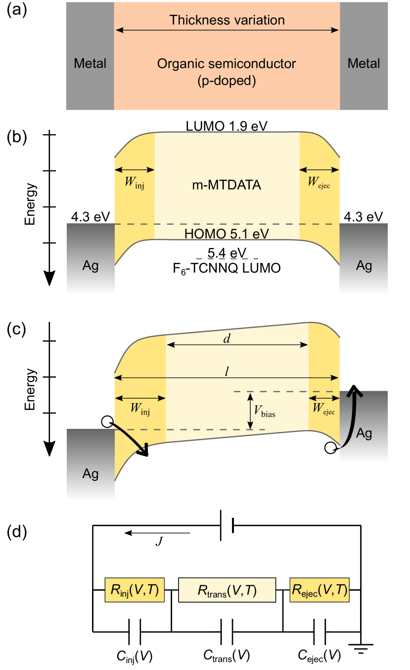
The minimal transport layer is chosen to be , as films below this thickness become increasingly prone to short-circuit failures. Furthermore, any spatial overlap of the two depletion regions must be avoided to keep the device physics clear. With typical values for our material system like the relative permittivity of a typical organic semiconductor [23], the intrinsic potential barrier at the interface , and the ionized acceptor concentration , the depletion width of one contact can be estimated at to range around .
| (1) |
The depletion width additionally depends on the applied bias, as schematically indicated in Fig. 1(c). Still, a minimum transport layer thickness of safely rules out depletion region interference.
The utilization of a single doped organic film guarantees a very homogeneous current density and electric field distributions within the device, which is not compromised by additional intrinsic layers or organic-organic interfaces in the film [41, 42]. This is proven by current density over voltage () measurements for different sample areas, which were all found to coincide closely, cf. SI Sect. \Romannum4. For the experiments presented throughout this study, we used the smallest realized cross-section area of to resolve the lowest possible current densities and to prevent self heating-induced inhomogeneities scaling with active area dimension [43].
II.2 Resistance measurements
A four-wire scan is run back and forth in a Peltier element-based cryostat under vacuum (below ) to ensure stable thermal conditions. Details about the four-wire setup are introduced in Ref. [44]. The technique enables more accurate measurements excluding external series resistances that jeopardize a precise capacitance analysis. This is essential for observing the intended characteristics.
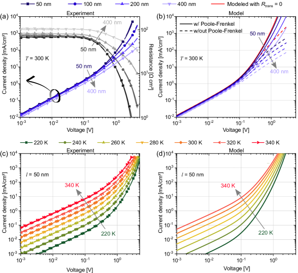
Figure 2(a) presents the measurement results for all four devices at a constant temperature . The blue-shaded lines show the characteristics and the grayscale curves the same data set in resistance representation . Only a very slight hysteresis, which is scaling with increasing current density, is detected. It can be identified more clearly in Fig. S2. Electrothermal feedback, which causes a deviation between backward and forward measurement directions, can therefore be rendered unimportant for the overall data analysis [44].
For , the curves of the four different transport layer thicknesses differ only slightly. This indicates that they are governed by the contact resistance between metal and doped organic semiconductor at low voltages. If the transport resistance posed a major contribution, the transport layer variation by a factor of 8 would cause a respective line separation. This is not the case. While the device shows a slight current density and resistance deviation, the three thinnest devices can merely be kept apart.
For , the resistance of all devices plummets. Also, the lines start separating drastically according to their transport layer thickness, i.e. the contact resistance drops below the transport resistance which starts to govern the device characteristics.
Figure 1(d) presents an equivalent circuit that can be used to better understand this behavior. Any of the three introduced device layers, i.e. injection, transport, and ejection layer, needs to comprise a resistive component. The circuit model also emphasizes that our devices sport two contact resistances, one at each metal/organic film interface. The experiment, therefore, measures the sum of a forward and reverse contact resistance contribution.
Ejection and injection interfaces each need to be represented by a variable resistor and , as all devices are limited by their contact resistances at low bias voltages. Instead of an accurate but complex interface analysis, only the governing physical concepts are included. This is sufficient to understand the device physics, as we see that our model successfully represents all experimental trends. Accurate quantitative tracing of the experimental results is not our intention here. The charge carrier injection and ejection currents can be understood as Schottky contacts and are described by a tunneling term [45] and an ideal diode equation [10], which is reduced by the effective, i.e. image force-reduced, potential barrier at the interface .
| (2) | |||
| (3) |
The parameter depicts the Boltzmann constant, the device temperature, the diode ideality factor, the elementary charge, an arbitrary tunneling scaling factor, the voltage drop across the respective resistor element, the scale current density, and the scale conductivity. Please note that again yields a current density, which is the current density of the tunneling term. The global model parameters are given in Tab. 1.
The symmetric architecture yields a symmetric device behavior, as shown in the SI Fig. S2. So, both contacts need to be described by the same formula. We choose a simple superposition, which only differs in the respective signs for injection and ejection current densities.
| (4) | |||
| (5) |
Both contact elements are susceptible to the voltage drop across the respective interface and decrease exponentially, as found by the experimental data. An increasing bias causes a more pronounced band bending at the injection interface, which increases the tunneling probability. Also, the Schottky barrier at the ejection interface is reduced [46]. Both processes make the total contact resistance drop with increasing bias voltage.
The transport resistance must also be represented by a variable resistor element , since the devices depend on the thickness of the organic film at elevated bias voltages. Due to the high doping concentration throughout the entire organic semiconductor film, space charge-limited effects cannot play a pivotal part and the transport resistance is assumed to be purely Ohmic. Please be referred to the SI Sect. \Romannum2 for the detailed reasoning. The current density passing reads
| (6) |
with being the thickness of the non-depleted transport layer and the total thickness of the doped organic film, cf. Fig. 1 (c), the voltage drop across the transport layer, and temperature-activated ionized dopant concentration, equal to the effective charge carrier density, cf. SI Sect. \Romannum1 and the parameters in Tab. 1.
| (7) |
As temperature- and field-dependent experiments are carried out and alter the device characteristics, the mobility term must contain a temperature and an electric field dependency to successfully model the experimental results. has to drop with increasing bias, since the curves bend upwards when separated according to their transport layer thickness. This cannot be explained by linear resistance characteristics. The behavior at high electric fields, here exceeding , requires a field-induced mobility enhancement, commonly known as Poole-Frenkel (P-F) effect [45, 11].
| (8) | |||
| (9) |
The parameter is defined in Ref. [47], is the Boltzmann constant, the device temperature, the relative permittivity of the organic film, and the mobility activation energy. For both dependencies, temperature and electric field, we used simplistic approaches. We are well aware that both dependencies have to be modeled with more complexity if a good agreement between experimental and model results is expected. Our model fails at high electric fields, as can be seen by the increasing deviations between Figs. 2(a) and (b). This accounts for an oversimplification of the P-F term in the equivalent circuit. From the simulated results in Fig. 2(b), comprising both a scenario with and without P-F term, one can estimate the true P-F contribution to be in between the two realized modeling scenarios, i.e. a reduction of would yield better agreements. Pursuing this, however, is not the intention of our investigation. It is yet worth to point out that our presented experimental approach allows studying the P-F effect in organic semiconductors with utmost precision. While stacked films in complete semiconductor devices induce a varying electric field in the vertical direction, the geometry realized here ensures a very homogeneous field strength throughout the transport layer.
The thinner the transport layer, the smaller its resistance contribution. A thinner device follows the pure contact resistance characteristics up to higher current densities than a thick device. Hence, the isolated contact resistance can be estimated best from the sample. Figure 2(b) presents the model scenario with vanishing transport influence, , indicated in red. It is, therefore, safe to deduce that the contact resistance characteristics must be nonlinear and stays reasonably close to the device up to about . This range is sufficient to quantify the contact resistance for most organic electronics applications.
Both contact resistance and transport characteristics are susceptible to temperature, which is presented in Fig. 2(c) and (d). That is, the mobility in eq. (8) is enhanced by an Arrhenius term, as are the tunneling and diode characteristics in eqs. (2) and (3). The experimental trend of temperature-induced conductivity is replicated successfully by the model.
The simulation of the three resistance contributions displayed in Fig. 1(d) is evaluated with LTspice and allows to quantify each of them separately. Figure S9 presents the modeled contributions and makes it plain that the injection and ejection resistances govern the device behavior at low voltages. For all three resistances start to drop dramatically. The two contact resistance contributions and , however, drop faster than the transport resistance, which takes over the device characteristics at increasing bias. Figure S9 also implies that injection and ejection follow roughly the same trend at low voltages, owing to their mutual exponential nature. Thus, an estimation to identify either the injection (important for OLEDs) or ejection resistance (important for PV) from the measurements would be at low voltages.
II.3 Impedance measurements
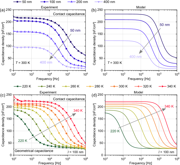
To gather further evidence that the pure contact behavior is disclosed in the presented devices, impedance measurements are performed. Figures 3(a) and (c) present the experimental capacitance density over frequency characteristics () at zero bias voltage with varying thickness and temperature, respectively. Please find the details on capacitance density evaluation from a four-wire measurement in the SI Sect. \Romannum5. Again, it is very important to employ a four-wire measuring technique to keep parasitic series resistance out of the evaluation.
The experimental results present two distinct capacitance density plateaus. This behavior can be understood if treating any of the three distinct layers within the device not only as having a resistive representation but as an RC element, cf. Fig. 1(d). At , the depletion regions of injection and ejection have the same width and, treated like plate capacitors in the equivalent circuit, also the same capacitance density .
| (10) | |||
| (11) |
At low frequencies, the reactance of the transport capacitance is high and the charge carrier flow is mediated rather via . As a result, the device capacitance is governed by the injection and ejection capacitances. At room temperature, with no bias voltage, negligible transport resistance, and low frequencies, the device capacitance density can be estimated as
| (12) |
with due to device symmetry at . From Fig. 3(a), however, it is apparent that eq. (12) holds merely for low transport resistances, i.e. very thin transport layers. The thicker the transport layer, the higher its resistance. As a result, even at low frequencies the transport capacitance mediates a significant share of the device current and reduces the total capacitance density. Thus, the capacitance at low frequencies is decreasing with increasing transport layer thickness and the pure contact capacitance can only be measured for transport layers striving toward zero thickness, i.e. the device.
At high frequencies, the transport capacitance becomes dominant as its reactance drops below the resistance of the transport layer. Since the depletion region is smaller than the transport layer thickness of all devices, cf. eq. (1), the contact capacitance is expected to be higher than the transport capacitance. As a result, the total capacitance density falls to a second plateau at high frequencies. This plateau is governed by the device geometry (organic film thickness) and is called the geometrical capacitance density .
| (13) |
The transport capacitance density is a function of the transport layer thickness and is, as a simplistic approach, also represented by a plate capacitor in the equivalent circuit given in Fig. 1(d).
| (14) |
To support the just-presented understanding, the impedance spectroscopy was also carried out with a fixed organic film thickness () for different temperatures. Figure 3(c) presents the transition interval between the contact and the geometrical capacitance density plateau as being temperature-dependent. This can be mainly understood by considering as a function of temperature according to eqs. (6) and (8). At low temperatures, is high and the current is mediated earlier via the transport capacitance, whose reactance does not scale directly with temperature. For increasing temperatures, decreases and the cut-off frequency for the transport RC element increases.
| (15) |
Figures 3(b) and (d) present the results from the equivalent circuit model performed with LTspice. The qualitative trends of the experiments are reproduced and even quantitatively the results are similar. The transition characteristics in the experiment, however, are sloping more gently than in the model. The equivalent circuit follows the Schottky assumption of three distinct layers having an abrupt change from depleted to neutral semiconductor characteristics. This is a simplification that allows modeling the two different, frequency-dependent operating regimes. In the real device, however, the transition between depleted and neutral regions is smooth and hence the impedance characteristics are smeared out with respect to the model.
II.4 Depletion zone variation
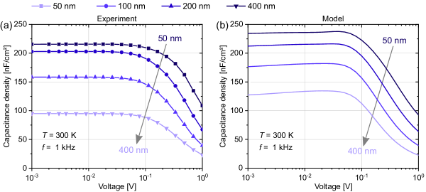
The impedance spectroscopy experiments discussed above were performed at zero bias voltage . Here, the contact capacitances at either side of the device must be equal, according to the device’s symmetry. The depletion width , however, depends on the voltage drop over the respective layer, cf. eq. (1) and Fig. 1(c). The idea of the subsequent measurement is to investigate the influence of voltage on the contact capacitances.
To access the isolated contact capacitance characteristics as well as possible, the experiment is performed at and room temperature, as deduced from the last section. Figure 4(a) presents the capacitance density of all four devices over the applied bias voltage. Using the global set of model parameters displayed in Tab. 1, a short-circuit depletion width of about at each interface can be expected. According to eq. (1) and as indicated in Fig. 1(c), increases and decreases under forward bias. When considering the contact-limited capacitance at , where the transport capacitance density is assumed to play no pivotal role, the capacitance density trend can be understood to follow
| (16) |
with both and following eq. (1). For low applied bias, both voltage dependencies apparently cancel each other, as around their behavior can be approximated as being linear. Beyond an applied bias of about , the linear approximation fails, and the denominator of eq. (16) starts to grow. The total capacitance density of the devices drops. The same overall trend can be reproduced by the equivalent circuit simulation, presented in Fig. 4(b).
II.5 Demonstration scenario for injection enhancement quantification
Throughout the sections, an experimental setting was introduced that evidently provides direct access to the contact resistance of a given interface between a metal and a doped organic film. As an outline towards potential application scenarios, this section presents a short study on the effect of additional interface layers that reduce the contact resistance.
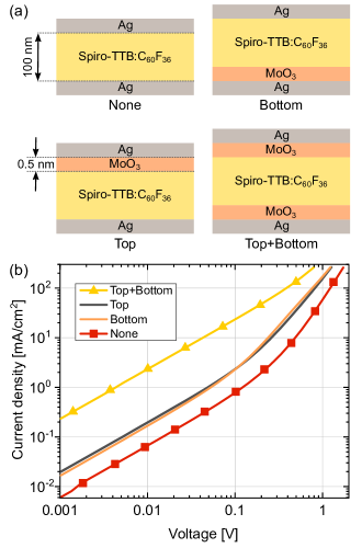
The subsequent experiment uses an equivalently simple stack of of Spiro-TTB doped with \ceC60F36 () sandwiched between two silver electrodes. Again, we performed a thickness-dependent analysis and found like for the m-MTDATA:\ceF6-TCNNQ devices that the resistance behavior for is not influenced by the organic layer thickness up to , cf. SI Sect. \Romannum6. That is, direct access to the device’s contact resistance is guaranteed. Now, either at the top, the bottom, or both contact interfaces a thin layer () of molybdenum oxide () is added, cf. Fig. 5(a), which is commonly used to reduce the contact resistance of p-doped organic semiconductor devices [48, 49, 4, 50, 15]. The data in Fig. 5(b) proves that adding one injection interlayer clearly reduces the contact resistance of the respective interface. There appears to be no significant difference between employing the enhancement layer in the top or bottom configuration. Most likely, the non-enhanced contact governs the contact resistance characteristics here. Using \ceMoO3 on both interfaces reduces the contact resistance at by more than one order of magnitude from about to below . A detailed investigation of this material combination can be found in the SI Sect. \Romannum6. In such a fashion, contact resistance enhancing strategies can easily be evaluated.
III Conclusion
This article presents a strategy to measure the isolated contact resistance between metals and doped organic semiconductors up to reasonable device operating conditions. For the investigated model structure of a p-doped film (\cem-MTDATA:\ceF6-TCNNQ, ) between to silver electrodes, the two metal-organic interfaces cause a potential drop of about at . At this current density, one contact poses therefore a resistance of . The presented conception requires neither complex experiments nor sophisticated theoretical treatment but is based entirely on an easy-to-perform scan. As a proof of concept, we perform a thorough evaluation for the mentioned hole-only device configuration. We employ resistance and impedance measurements while scanning a variety of device temperatures and organic film thicknesses and successfully compare the results to a simple equivalent circuit realized in LTspice. The model uses one global set of parameters replicating all experimental findings. This proves that the measured device characteristics directly disclose the contact behavior of the device up to about for the given system, which is sufficient for most operating scenarios in LEDs or solar cells. We further present how our measurement concept can help other groups evaluate their contact enhancement strategies by investigating the influence of molybdenum oxide as an injection layer in a second material system comprising Spiro-TTB doped with \ceC60F36 and silver electrodes. The presented device architecture turns out to achieve extremely strong and homogeneous electric fields, which allows to specifically study the Poole-Frenkel effect in organic semiconductors.
IV Methods
IV.1 Device fabrication
The hole-only devices were fabricated by thermal evaporation under high vacuum (Kurt J. Lesker Company, evaporation pressure ) on glass substrates (Schott Borofloat33 glass, Prince Optics) of thickness. The substrates were cleaned in an ultrasonic bath with acetone, ethanol, and deionized water. Aluminum (Chempur) and silver (M&K GmbH Jena), each, are used as bottom and top electrodes. Only the silver contacts are drawn in Fig. 1 for simplicity. The p-layer consists of m-MTDATA (Synthon, sublimation cleaned) doped with \ceF6-TCNNQ (Novaled AG, sublimation cleaned) at a ratio of , or Spiro:TTB (Lumtec, sublimation cleaned) doped with \ceC60F36 (Ionic Liquids Technologie GmbH, sublimation cleaned) also at . The thickness and deposition rates were monitored using a quartz crystal microbalance. Please find the full names of the materials and reverse characteristics in the SI Sect. \Romannum1 and \Romannum3.
To prohibit air and moisture contamination, the device stacks were encapsulated under nitrogen atmosphere after fabrication. The encapsulation glass (Sodalime glass, AMGTECH Korea) comprises a small cavity above the pixels that prevents direct contact between sensitive materials and the encapsulation glass. It was attached to the substrate using an epoxy resin (XNR5516Z-L and XNR5590, Nagase Europa GmbH).
IV.2 Device evaluation
The devices were placed in a Peltier element-equipped cryostat that is controlled by a temperature controller (Belektronig, HAT control). The air pressure inside the cryostat was reduced to below using a pre-vacuum pumping system (Trivac D16B, Germany) to keep a steady temperature and preventing unwanted air convection. Every measurement was performed using the four-wire method run by a dual-channel SMU (Keithley 2602). Impedance measurements were performed using an LCR meter (Hewlett Packard 4284A precision LCR meter) and a home-built switching matrix to switch between SMU und LCR and target individual device pixels. Temperature controller, LCR meter, and SMU were run and controlled by the software tool SweepMe! [51], which enables automated measurement protocols.
IV.3 Equivalent circuit modeling
The software LTspice (Linear Technology) was used for modeling the equivalent circuit presented in Fig. 1(d) with one fixed set of parameters to achieve all model results, cf. Tab. 1. In contrast to an analytical Python code, LTspice can self-consistently iterate solutions to model voltage dependent impedance measurements, as presented in Fig. 4.
| Diode ideality factor | 1 | |
|---|---|---|
| Tunneling scaling factor | ||
| Tunneling scale conductivity | ||
| Diode scale current density | ||
| Interface potential barrier | ||
| Scale mobility | ||
| Scale doping concentration | ||
| Relative permittivity | ||
| Doping activation energy | ||
| Mobility activation energy |
References
- Guo et al. [2016] Y. Guo, W. Sato, K. Shoyama, and E. Nakamura, Sulfamic Acid-Catalyzed Lead Perovskite Formation for Solar Cell Fabrication on Glass or Plastic Substrates, Journal of the American Chemical Society 138, 5410 (2016).
- Trukhanov et al. [2011] V. A. Trukhanov, V. V. Bruevich, and D. Y. Paraschuk, Effect of doping on performance of organic solar cells, Physical Review B 84, 205318 (2011).
- Xiao et al. [2017] J.-W. Xiao, C. Shi, C. Zhou, D. Zhang, Y. Li, and Q. Chen, Contact Engineering: Electrode Materials for Highly Efficient and Stable Perovskite Solar Cells, Solar RRL 1, 1700082 (2017).
- Ding and Forrest [2020] K. Ding and S. R. Forrest, Reducing Energy Losses at the Organic–anode-buffer Interface of Organic Photovoltaics, Physical Review Applied 13, 054046 (2020).
- Yahya and Fadavieslam [2021] M. Yahya and M. R. Fadavieslam, The effects of argon plasma treatment on ITO properties and the performance of OLED devices, Optical Materials 120, 111400 (2021).
- Khan et al. [2019] M. T. Khan, M. Salado, A. Almohammedi, S. Kazim, and S. Ahmad, Elucidating the Impact of Charge Selective Contact in Halide Perovskite through Impedance Spectroscopy, Advanced Materials Interfaces 6, 1901193 (2019).
- Wei et al. [2022] H. Wei, R. Zhang, G. Huang, C. Lv, and J. Tang, Highly stable and efficient tandem white light emitting diodes based on efficient electron injection and transport, Journal of Materials Chemistry C 10.1039/D1TC05687E (2022).
- Waldrip et al. [2020] M. Waldrip, O. D. Jurchescu, D. J. Gundlach, and E. G. Bittle, Contact Resistance in Organic Field-Effect Transistors: Conquering the Barrier, Advanced Functional Materials 30, 1904576 (2020).
- Dollinger et al. [2019] F. Dollinger, K.-G. Lim, Y. Li, E. Guo, P. Formánek, R. Hübner, A. Fischer, H. Kleemann, and K. Leo, Vertical Organic Thin-Film Transistors with an Anodized Permeable Base for Very Low Leakage Current, Advanced Materials 31, 1900917 (2019).
- Sze et al. [2021] S. M. Sze, Y. Li, and K. K. Ng, Physics of Semiconductor Devices (John Wiley & Sons, 2021).
- Köhler and Bässler [2015] A. Köhler and H. Bässler, Electronic Processes in Organic Semiconductors: An Introduction (Wiley-VCH, 2015).
- Forrest [2020] S. R. Forrest, Organic Electronics: Foundations to Applications (OUP Oxford, 2020).
- Kumatani et al. [2013] A. Kumatani, Y. Li, P. Darmawan, T. Minari, and K. Tsukagoshi, On Practical Charge Injection at the Metal/Organic Semiconductor Interface, Scientific Reports 3, 1026 (2013).
- Kumaki et al. [2008] D. Kumaki, T. Umeda, and S. Tokito, Reducing the contact resistance of bottom-contact pentacene thin-film transistors by employing a MoOx carrier injection layer, Applied Physics Letters 92, 013301 (2008).
- Kotadiya et al. [2018] N. B. Kotadiya, H. Lu, A. Mondal, Y. Ie, D. Andrienko, P. W. M. Blom, and G.-J. A. H. Wetzelaer, Universal strategy for Ohmic hole injection into organic semiconductors with high ionization energies, Nature Materials 17, 329 (2018).
- Kahn et al. [2003] A. Kahn, N. Koch, and W. Gao, Electronic structure and electrical properties of interfaces between metals and -conjugated molecular films, Journal of Polymer Science Part B: Polymer Physics 41, 2529 (2003).
- Auroux et al. [2021] E. Auroux, A. Sandström, C. Larsen, E. Zäll, P. Lundberg, T. Wågberg, and L. Edman, Evidence and Effects of Ion Transfer at Active-Material/Electrode Interfaces in Solution-Fabricated Light-Emitting Electrochemical Cells, Advanced Electronic Materials 7, 2100253 (2021).
- Walzer et al. [2007] K. Walzer, B. Maennig, M. Pfeiffer, and K. Leo, Highly Efficient Organic Devices Based on Electrically Doped Transport Layers, Chemical Reviews 107, 1233 (2007).
- Tietze et al. [2012] M. L. Tietze, L. Burtone, M. Riede, B. Lüssem, and K. Leo, Fermi level shift and doping efficiency in $p$-doped small molecule organic semiconductors: A photoelectron spectroscopy and theoretical study, Physical Review B 86, 035320 (2012).
- Tietze et al. [2018] M. L. Tietze, J. Benduhn, P. Pahner, B. Nell, M. Schwarze, H. Kleemann, M. Krammer, K. Zojer, K. Vandewal, and K. Leo, Elementary steps in electrical doping of organic semiconductors, Nature Communications 9, 1182 (2018).
- Limketkai and Baldo [2005] B. N. Limketkai and M. A. Baldo, Charge injection into cathode-doped amorphous organic semiconductors, Physical Review B 71, 085207 (2005).
- Hosseini et al. [2005] A. R. Hosseini, M. H. Wong, Y. Shen, and G. G. Malliaras, Charge injection in doped organic semiconductors, Journal of Applied Physics 97, 023705 (2005).
- Brütting et al. [2012] W. Brütting, C. Adachi, and R. J. Holmes, Physics of Organic Semiconductors, 2nd ed. (Wiley-VCH, 2012).
- Liaptsis and Meerholz [2013] G. Liaptsis and K. Meerholz, Crosslinkable TAPC-Based Hole-Transport Materials for Solution-Processed Organic Light-Emitting Diodes with Reduced Efficiency Roll-Off, Advanced Functional Materials 23, 359 (2013).
- Züfle et al. [2017] S. Züfle, S. Altazin, A. Hofmann, L. Jäger, M. T. Neukom, W. Brütting, and B. Ruhstaller, Determination of charge transport activation energy and injection barrier in organic semiconductor devices, Journal of Applied Physics 122, 115502 (2017).
- Siemund and Göbel [2016] H. Siemund and H. Göbel, Numerical Simulation of Organic Light-Emitting Diodes With Insulating Cathode Buffer Layer, IEEE Transactions on Electron Devices 63, 3700 (2016).
- Meister et al. [2018] S. Meister, R. Brückner, M. Sudzius, H. Fröb, and K. Leo, Optically pumped lasing of an electrically active hybrid OLED-microcavity, Applied Physics Letters 112, 113301 (2018).
- Meerheim et al. [2006] R. Meerheim, K. Walzer, G. He, M. Pfeiffer, and K. Leo, Highly efficient organic light emitting diodes (OLED) for diplays and lighting, in Photonics Europe, edited by P. L. Heremans, M. Muccini, and E. A. Meulenkamp (Strasbourg, France, 2006) p. 61920P.
- Meerheim et al. [2008] R. Meerheim, S. Scholz, S. Olthof, G. Schwartz, S. Reineke, K. Walzer, and K. Leo, Influence of charge balance and exciton distribution on efficiency and lifetime of phosphorescent organic light-emitting devices, Journal of Applied Physics 104, 014510 (2008).
- Borchert et al. [2022] J. W. Borchert, R. T. Weitz, S. Ludwigs, and H. Klauk, A Critical Outlook for the Pursuit of Lower Contact Resistance in Organic Transistors, Advanced Materials 34, 2104075 (2022).
- Sandberg et al. [2016] O. J. Sandberg, A. Sundqvist, M. Nyman, and R. Österbacka, Relating Charge Transport, Contact Properties, and Recombination to Open-Circuit Voltage in Sandwich-Type Thin-Film Solar Cells, Physical Review Applied 5, 044005 (2016).
- Altazin et al. [2011] S. Altazin, R. Clerc, R. Gwoziecki, D. Boudinet, G. Ghibaudo, G. Pananakakis, I. Chartier, and R. Coppard, Analytical modeling of the contact resistance in top gate/bottom contacts organic thin film transistors, Organic Electronics 12, 897 (2011).
- Oehzelt et al. [2014] M. Oehzelt, N. Koch, and G. Heimel, Organic semiconductor density of states controls the energy level alignment at electrode interfaces, Nature Communications 5, 4174 (2014).
- Olthof et al. [2009] S. Olthof, W. Tress, R. Meerheim, B. Lüssem, and K. Leo, Photoelectron spectroscopy study of systematically varied doping concentrations in an organic semiconductor layer using a molecular p-dopant, Journal of Applied Physics 106, 103711 (2009).
- Reeves and Harrison [1982] G. Reeves and H. Harrison, Obtaining the specific contact resistance from transmission line model measurements, IEEE Electron Device Letters 3, 111 (1982).
- Rhee and Yun [2008] S.-W. Rhee and D.-J. Yun, Metal–semiconductor contact in organic thin film transistors, Journal of Materials Chemistry 18, 5437 (2008).
- Horowitz [2011] G. Horowitz, Interface Modification for Tuning the Contact Resistance of Metal/Organic Semiconductor Junctions, The Open Applied Physics Journal 4, 2 (2011).
- Aonuma et al. [2007] M. Aonuma, T. Oyamada, H. Sasabe, T. Miki, and C. Adachi, Material design of hole transport materials capable of thick-film formation in organic light emitting diodes, Applied Physics Letters 90, 183503 (2007).
- Michaelson [1977] H. B. Michaelson, The work function of the elements and its periodicity, Journal of Applied Physics 48, 4729 (1977).
- Koech et al. [2010] P. K. Koech, A. B. Padmaperuma, L. Wang, J. S. Swensen, E. Polikarpov, J. T. Darsell, J. E. Rainbolt, and D. J. Gaspar, Synthesis and Application of 1,3,4,5,7,8-Hexafluorotetracyanonaphthoquinodimethane (F6-TNAP): A Conductivity Dopant for Organic Light-Emitting Devices, Chemistry of Materials 22, 3926 (2010).
- Zheng et al. [2019] Y. Zheng, A. Fischer, N. Sergeeva, S. Reineke, and S. C. B. Mannsfeld, Exploiting lateral current flow due to doped layers in semiconductor devices having crossbar electrodes, Organic Electronics 65, 82 (2019).
- Fischer et al. [2012] A. Fischer, P. Pahner, B. Lüssem, K. Leo, R. Scholz, T. Koprucki, J. Fuhrmann, K. Gärtner, and A. Glitzky, Self-heating effects in organic semiconductor crossbar structures with small active area, Organic Electronics 13, 2461 (2012).
- Kirch et al. [2021] A. Kirch, A. Fischer, M. Liero, J. Fuhrmann, A. Glitzky, and S. Reineke, Electrothermal Tristability Causes Sudden Burn-In Phenomena in Organic LEDs, Advanced Functional Materials 31, 2106716 (2021).
- Kirch et al. [2020] A. Kirch, A. Fischer, M. Liero, J. Fuhrmann, A. Glitzky, and S. Reineke, Experimental proof of Joule heating-induced switched-back regions in OLEDs, Light: Science & Applications 9, 1 (2020).
- Wang et al. [2010] Z. B. Wang, M. G. Helander, M. T. Greiner, J. Qiu, and Z. H. Lu, Carrier mobility of organic semiconductors based on current-voltage characteristics, Journal of Applied Physics 107, 034506 (2010).
- Pahner et al. [2013] P. Pahner, H. Kleemann, L. Burtone, M. L. Tietze, J. Fischer, K. Leo, and B. Lüssem, Pentacene Schottky diodes studied by impedance spectroscopy: Doping properties and trap response, Physical Review B 88, 195205 (2013).
- Murgatroyd [1970] P. N. Murgatroyd, Theory of space-charge-limited current enhanced by Frenkel effect, Journal of Physics D: Applied Physics 3, 151 (1970).
- Wang et al. [2008] F. Wang, X. Qiao, T. Xiong, and D. Ma, The role of molybdenum oxide as anode interfacial modification in the improvement of efficiency and stability in organic light-emitting diodes, Organic Electronics 9, 985 (2008).
- Matsushima et al. [2008] T. Matsushima, G.-H. Jin, and H. Murata, Marked improvement in electroluminescence characteristics of organic light-emitting diodes using an ultrathin hole-injection layer of molybdenum oxide, Journal of Applied Physics 104, 054501 (2008).
- Meyer and Kahn [2011] J. Meyer and A. L. Kahn, Electronic structure of molybdenum-oxide films and associated charge injection mechanisms in organic devices, Journal of Photonics for Energy 1, 011109 (2011).
- Fischer and Kaschura [2020] A. Fischer and F. Kaschura, SweepMe! A multi-tool measurement software, www.sweep-me.net (2020).
Acknowledgements
This work was supported by the German Research Foundation (DFG) within the project HEFOS (Grant No. FI 2449/1-1) and EFOD (Grant No. RE 3198/6-1). The authors thank Andreas Wendel and Tobias Günther for manufacturing the devices.
V Author contributions
A.F. conceptualized the study. A.K. and A.F. analyzed the data and performed the LTspice implementation. A.K. prepared the graphs and mainly wrote the manuscript. A.F., R.W., P.I. and K.M. set up and conducted the experiments. J.B. and S.M. contributed major ideas to the physical understanding. S.R. supervised the project. All authors discussed the results, reviewed the manuscript, and contributed to the text.
VI Competing interests
Dr. Axel Fischer is co-founder of “SweepMe! GmbH” which provided the measurement software “SweepMe!” (sweep-me.net). The name of the program is given in the manuscript. The other authors declare no conflicts of interest.
VII Materials and Correspondence
All material, code and data is available on reasonable request.