Huge out-of-plane piezoelectric response in ferromagnetic monolayer NiClI
Abstract
The combination of piezoelectricity and ferromagnetic (FM) order in a two-dimensional (2D) material, namely 2D piezoelectric ferromagnetism (PFM), may open up unprecedented opportunities for novel device applications. Here, we predict an in-plane FM semiconductor Janus monolayer NiClI with considerably large magnetic anisotropy energy (MAE) of 1.439 meV, exhibiting dynamic, mechanical and thermal stabilities. The NiClI monolayer possesses larger in-plane piezoelectricity (5.21 pm/V) comparable to that of . Furthermore, NiClI has huge out-of-plane piezoelectricity (1.89 pm/V), which is highly desirable for ultrathin piezoelectric device application. It is proved that huge out-of-plane piezoelectricity is robust against electronic correlation, which confirms reliability of huge . Finally, being analogous to NiClI, PFM with large out-of-plane piezoelectricity can also be achieved in the Janus monolayers of NiClBr and NiBrI, with the predicted of 0.73 pm/V and 1.15 pm/V, respectively. The predicted huge out-of-plane piezoelectric response makes Janus monolayer NiClI a good platform for multifunctional semiconductor spintronic applications, which is also compatible with the bottom/top gate technologies of conventional semiconductor nanoelectronic devices.
I Introduction
Two-dimensional (2D) materials can exhibit significantly different and novel properties compared to their bulk counterpartsq1 ; q2 ; q4-1 ; q4 . A particularly useful property is piezoelectricity, which can convert mechanical energy into electrical energy and vice versaq4-1 ; q4 . The piezoelectricity of 2D materials has been widely investigated in recent years. Experimentally, the piezoelectricity has been confirmed in multiple 2D materials, such as q8-1 , q5 ; q6 and MoSSeq8 , thus concretely establishing the feasibility of 2D-material-based piezoelectric device technology. Theoretically, a large number of 2D materials have been predicted to be piezoelectric, including transition metal dichalchogenides (TMD), Janus TMD, , group IIA and IIB metal oxides, group-V binary semiconductors and group III-V semiconductorsq7 ; q7-1 ; q7-2 ; q7-3 ; q7-4 ; q7-5 ; q7-6 ; q7-7 . A substantial in-plane piezoelectricity can be observed in many 2D materialsq7 ; q7-2 ; q7-3 ; q7-4 ; q7-5 , while an out-of-plane piezoelectric response is typically very smallq7 ; q7-2 (For most of them, the is less than 1 pm/V). Thus, searching for large out-of-plane piezoelectric response in 2D materials has become an important quest, particularly due to its compatibility with bottom/top gate device architecture of many conventional semiconductor devices.
The multifunctional 2D piezoelectric materials, such as coexistence of piezoelectricity and electronic topology or/and ferromagnetism or/and valley, are of particular interest, which can provide a potential platform for multi-functional electronic devices. The PFMs have been predicted in 2D vanadium dichalcogenides, , and qt1 ; q15 ; q15-1 ; q15-2 . The piezoelectric quantum anomalous Hall insulator (PQAHI), which combines piezoelectricity with topological and FM orders, has been reported in Janus monolayer (X=Cl and Br)gsd1 . This provides possibility to use the piezoelectric effect to control quantum anomalous Hall (QAH) effects. The piezoelectric ferrovalley (FV) material has been proposed in monolayergsd2 , and the anomalous valley Hall effect may be achieved by piezoelectric effect. Therefore, the search of high-performance 2D piezoelectric materials is a critical step that may open new opportunities towards the development of novel nanodevice applications.
Multifunctional 2D piezoelectric materials with large out-of-plane piezoelectric response has received strong research attention in recent years. Magnetic monolayer metal halides (M=V, Cr, Mn, Fe, Co and Ni; X=Cl, Br and I) with 1T crystal structure ( symmetry) have been investigated from first-principles and Monte Carlo simulations, and (X=Cl, Br and I) of them are FM semiconductors with excellent stabilitye ; e1 . Due to the inversion symmetry, (X=Cl, Br and I) monolayers are not piezoelectric. Janus 2D materials with breaking mirror or inversion symmetry along out-of-plane orientations provide possibility to achieve out-of-plane piezoelectric response. Based on , Janus monolayer MoSSe has been successfully synthesised by various experimental synthesis strategiesq8 ; e2 .
Motivated by the successful demonstration of strong out-of-plane piezoelectric response in Janus system, we explore the electronic and piezoelectric properties of Janus NiClI monolayer, which can be constructed from / monolayer. It is found that NiClI monolayer is an in-plane FM semiconductor with large MAE of 1.439 meV, exhibiting good stability. The NiClI monolayer not only possesses large in-plane piezoelectricity (5.21 pm/V), but also has huge out-of-plane piezoelectricity (1.89 pm/V). Calculated results show that the excellent piezoelectricity is robust against electronic correlation. Finally, similar to NiClI, the PFMs with large out-of-plane piezoelectric response can also be realized in the monolayer NiClBr and NiBrI. These findings reveal the enormous potential of NiClI monolayer as a promising candidate materials for the development of novel 2D piezoelectric spintronic devices.
| Name | MAE | ||||||||
|---|---|---|---|---|---|---|---|---|---|
| 3.604 | 23.28 | -45 | 47.61 | 13.55 | 0.46 | 0.45 | 1.35 | 0.73 | |
| 3.855 | 24.91 | -749 | 41.95 | 12.21 | 0.74 | 0.62 | 2.49 | 1.15 | |
| 3.774 | 18.84 | -1439 | 42.33 | 13.41 | 1.51 | 1.05 | 5.21 | 1.89 |
II Computational detail
The density functional theory (DFT) calculations1 are performed by using the projector-augmented wave method as implemented in the plane-wave code VASPpv1 ; pv2 ; pv3 . The popular generalized gradient approximation of Perdew, Burke and Ernzerhof (GGA-PBE)pbe is adopted as the exchange-correlation functional. To consider on-site Coulomb correlation of Ni-3 electrons, the GGA+ scheme by the rotationally invariant approach proposed by Dudarev et alu is adopted with 4 eV, where only the effective () based on the difference between the on-site Coulomb interaction parameter and exchange parameters is meaningful. The spin-orbital coupling (SOC) effect is explicitly included in the calculations of MAE and electronic structures. The energy cut-off of 500 eV, total energy convergence criterion of eV and force convergence criteria of less than 0.0001 on each atom are adopted to attain reliable results. A vacuum space of more than 18 along the direction is adopted to avoid interactions between two neighboring images. The phonon dispersions are calculated through the direct supercell method with the 551 supercell, as implemented in Phonopy codepv5 . The coefficients of the elastic stiffness/piezoelectric stress tensors / are calculated by using strain-stress relationship (SSR)/density functional perturbation theory (DFPT) methodpv6 . The Brillouin zone sampling is done using a Monkhorst-Pack mesh of 21211 for , and 12211 for . The 2D elastic coefficients and piezoelectric stress coefficients have been renormalized by the the length of unit cell along direction (): = and =.
III Main calculated results
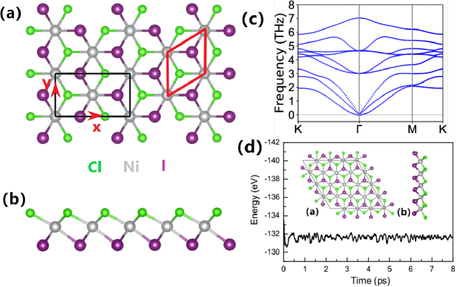
As shown in Figure 1 (a) and (b), the crystal structure of NiClI is formed by a Cl-Ni-I sandwich layer, and the Ni atom is surrounded by a distorted octahedron composed of three Cl and three I atoms. The NiClI monolayer can be constructed by replacing one of two Cl/I layers with I/Cl atoms in /. Due to the broken central symmetry, the symmetry of NiClI monolayer (No.156) is lower than that of / monolayer (No.164). Due to different electronegativities between Cl and I atoms, a natural vertical built-in electric field appears in the intralayer, which induces an out-of-plane piezoelectric response. The FM and antiferromagnetic (AFM) magnetic configurations are considered to ascertain the magnetic ground state of NiClI. The energy difference between AFM and FM orderings is 18.84 meV, indicating that the ground state of NiClI is FM. The optimized lattice constant is 3.774 , which is between ones of (3.518 ) and (3.983 )e1 .
As shown in Figure 1 (c), the phonon spectrum of NiClI shows no imaginary frequencies, indicating its dynamic stability. Two in-plane acoustic branches display linear dispersions, while out-of-plane acoustic branch shows a quadratic dispersion. These share general characteristics of 2D materials, when they are free of stressr1 ; r2 . To confirm the thermal stability, the evolution of total energy of NiClI as a function of simulation time is calculated using ab initio molecular dynamics (AIMD) with a 441 supercell in the canonical ensemble for 8 ps with a time step of 1.0 fs, which is plotted in Figure 1 (d). During the simulation period, the frameworks of NiClI are well preserved with little energy fluctuation, confirming its thermal stability. The elastic constants ( =42.33 and =13.41 ) of NiClI meet Born criteria of mechanical stability of a material with hexagonal symmetry ( and )ela , indicating its mechanical stability.
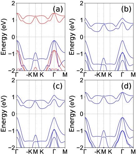
We show the spin-polarized energy band structures of NiClI in Figure 2 by using GGA and GGA+SOC. Figure 2 (a) shows a distinct spin splitting due to the exchange interaction, and NiClI is an indirect band gap semiconductor with gap of 1.00 eV. The valence band maximum (VBM)/conduction band bottom (CBM) is provided by the spin-up/spin-down, which is at /K (-K) point. It is noted that the energies of -K and K valleys are degenerate. As plotted in FIG.1 of electronic supplementary information (ESI), the Ni- projected band structures show that / orbitals dominate -K and K valleys of conduction band, which is very key to produce valley polarization. When the SOC is included, the spontaneous valley polarization can be observed, and the valley splitting of bottom conduction band is 49 meV. The K valley has higher energy than -K valley, and the valley polarization can be switched (The energy of -K valley is higher than one of K valley.) by reversing the magnetization direction, as shown in Figure 2 (c). It should be pointed out that / monolayer has no spontaneous valley polarization due to possessing centrosymmetry. Figure 2 (b) and (c) show that NiClI is still an indirect band gap semiconductor with gap value of 0.523 eV. As shown in Figure 2 (d), when the magnetization direction of NiClI is adjusted to positive direction, no valley polarization can be observed, and an indirect gap of 0.818 eV can be observed.
If the / orbitals dominate -K and K valleys, the valley splitting between -K and K points can be expressed asv2 ; v3 :
| (1) |
where is the strength of SOC. If the -K and K valleys are mainly from orbitals, the valley splitting is written as:
| (2) |
When the / orbitals dominate -K/K valley with the magnetization orientation being general case, v3 (=0/90∘ means out-of-plane/in-plane direction.). For in-plane magnetocrystalline direction, the valley splitting of NIClI monolayer will disappear.
Although the magnetocrystalline direction of NiClI monolayer can be regulated by external magnetic field, the intrinsic magnetic anisotropy should be determined. The MAE defined as energy difference (-) is calculated, where / is the energy per Ni atom when the magnetization is along the / direction. The positive value means out-of-plane direction, while the negative value suggests in-plane one. By using GGA+SOC, the calculated MAE is -1439 , which means that the intrinsic easy axis of NiClI is in-plane. So, NiClI monolayer is a common FM semiconductor, not a FV material.
The NiClI monolayer shows both in-plane and out-of-plane piezoelectric response due to special Janus structure. By performing symmetry analysis, only considering in-plane strain and stress, the piezoelectric stress, piezoelectric strain and elastic tensors of NiClI by using Voigt notation can be written asq7 ; q7-2 :
| (3) |
| (4) |
| (5) |
With an imposed uniaxial in-plane strain, both /0 and /0. However, when a biaxial in-plane strain is applied, /=0, but /0. Here, the two independent and can be derived by :
| (6) |
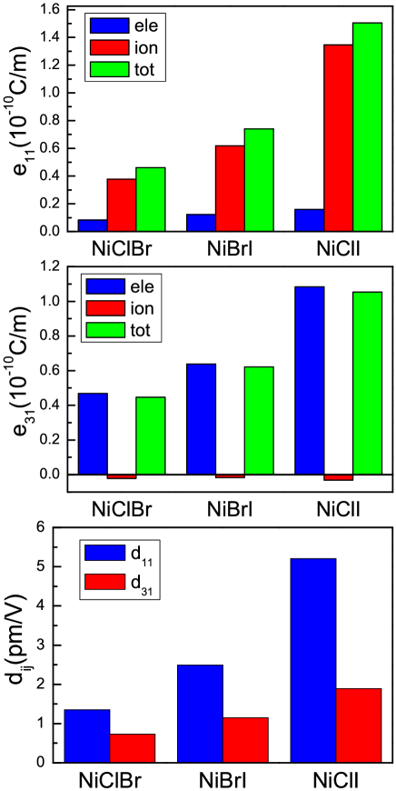
The orthorhombic supercell (see Figure 1) is adopted to calculate the / of NiClI. By DFPT method, the attained / is 1.51/1.05 C/m with ionic part 1.35/-0.03 C/m and electronic part 0.16/1.08 C/m. For , the electronic and ionic contributions have the same signs, and the ionic part dominates the piezoelectricity. However, for , the electronic and ionic contributions have opposite signs, and the electronic part plays a decisive role.
Based on Equation 6, the corresponding / of NiClI monolayer is 5.21/1.89 pm/V. To be compatible with the conventional bottom/top gate technologies, a large out-of-plane piezoelectric response is highly desired for 2D materials. The predicted of NiClI monolayer is higher than many 2D known materials, including the oxygen functionalized MXenes (0.40-0.78 pm/V)q9 , (1.72 pm/V)re-3 , Janus TMD monolayers (0.03 pm/V)q7 , functionalized h-BN (0.13 pm/V)o1 , Janus / monolayer (1.14-1.80 pm/V)q15-1 , kalium decorated graphene (0.3 pm/V)o2 , Janus group-III materials (0.46 pm/V)q7-6-1 , Janus BiTeI/SbTeI monolayer (0.37-0.66 pm/V)o3 , - (0.415 pm/V)o4 and MoSO (0.7 pm/V)re-11 . The of NiClI is lower than ones of TePtS/TePtSe (2.4-2.9 pm/V)re-6 and (2.58 pm/V)q15-1 . However, compared with TePtS/TePtSe, the coexistence of intrinsic piezoelectricity and ferromagnetism can be achieved in NiClI. With respect to , the NiClI has more higher . So, NiClI is a excellent PFM with huge out-of-plane piezoelectric response.
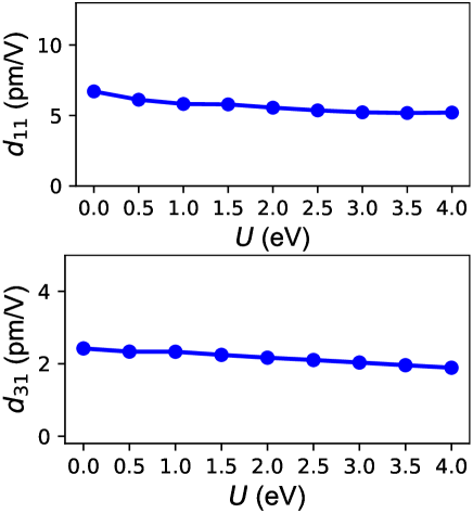
Electronic correlation has important effects on the electronic states and piezoelectric properties of 2D materialsgsd2 ; h10 ; h11 . To confirm the large in NiClI monolayer, electronic correlation effects on its piezoelectric properties are investigated. Firstly, we optimize lattice constants at different (0-4 eV) (see FIG.2 of ESI). The increases with increasing , and the change is very small (about 0.017 ). The energy difference between AFM and FM configurations as a function of is plotted in FIG.2 of ESI, which shows that NiClI is always a FM ground state. For both out-of-plane and in-plane magnetic anisotropy, the evolutions of electronic band structures as a function of are calculated by using GGA+SOC. The energy band structures at representative values are plotted in FIG.3 of ESI, and the gaps vs are shown in FIG.4 of ESI. It is clearly seen that NiClI changes from metal to semiconductor for out-of-plane magnetic anisotropy. However, NiClI is always a semiconductor for in-plane case within the considered range. To determine the intrinsic magnetic anisotropy, the MAE as a function of is plotted in FIG.5 of ESI, indicating an in-plane magnetic anisotropy within the considered range. Thus, NiClI is a FM semiconductor within the considered range, which is particularly beneficial for piezoelectric device applications where the strong suppression of leakage current is required.
The elastic constants (, , - and +) of NiClI monolayer as a function of are plotted in FIG.6 of ESI. It is found that these elastic constants have weak dependence on . The piezoelectric stress coefficients ( and ) along the ionic and electronic contributions vs are shown in FIG.7 of ESI. With increasing , both and of NiClI decrease, which leads to reduced and . The piezoelectric strain coefficients ( and ) of monolayer NiClI vs are plotted in Figure 3. It is found that reduced is in favour of enhanced and . At 0 eV, the and can improve to 6.71 pm/V and 2.42 pm/V. Thus, the large in NiClI monolayer is robust against electronic correlation.
IV Discussions and Conclusion
Janus monolayer NiClBr and NiBrI can also be constructed from (X=Cl, Br and I), which may possess large . According to calculated results in Table 1, the FM order is still the ground state of NiClBr and NiBrI by comparing the energy difference of AFM and FM magnetic configurations, and they possess in-plane magnetic anisotropy based on MAE. For monolayer NiClBr and NiBrI , the optimized lattice constants are 3.604 and 3.855 . The predicted and are 47.61 (41.95) and 13.55 (12.21) for NiClBr (NiBrI), satisfying Born criteria of mechanical stabilityela . Based on phonon dispersions in FIG.8 of ESI, it is proved that monolayer NiClBr and NiBrI are dynamically stable. The piezoelectric properties of monolayer NiClBr and NiBrI are investigated. The piezoelectric stress coefficients ( and ) along the ionic/electronic contribution and piezoelectric strain coefficients ( and ) of NiClBr, NiBrI and NiClI are plotted in Figure 4, and the corresponding data are summarized in Table 1. For all three monolayers, the electronic and ionic contributions of have the same signs, and the ionic part dominates the piezoelectricity. However, the electronic and ionic parts of have opposite signs, and the electronic part dominates the piezoelectricity with negligible ionic part. From NiClBr to NiBrI to NiClI, both and increase due to enhanced and . A piezoelectric material should be a semiconductor, and the energy band structures of NiClBr and NiBrI are plotted in FIG.9 of ESI with in-plane magnetic anisotropy. It is clearly seen that they are semiconductors.
In conclusion, based on first-principle calculations, the electronic structures and piezoelectric properties for Janus monolayer NiClI are investigated. For out-of-plane magnetic anisotropy, the NiClI is a FV material. However, a common FM semiconductor is observed for in-plane magnetic anisotropy. By calculating actual MAE, the easy axis of NiClI is in-plane. The calculated results show that NiClI monolayer has large piezoelectric response. Especially, the huge out-of-plane piezoelectricity with its =1.89 pm/V is achieved, which is significantly larger than those of most known 2D materials. Therefore, NiClI monolayer is suitable for ultrathin piezoelectric devices under the operating mode. It is found that the huge is robust against electronic correlation. Finally, similar to NiClI, monolayer NiClBr and NiBrI are also excellent PFMs with large being 0.73 pm/V and 1.15 pm/V. Our works offer useful material design guidelines to achieve PFMs with large out-of-plane piezoelectric response.
Acknowledgements.
This work is supported by the Natural Science Foundation of Shaanxi Provincial Department of Education (19JK0809). We are grateful to the Advanced Analysis and Computation Center of China University of Mining and Technology (CUMT) for the award of CPU hours and WIEN2k/VASP software to accomplish this work.References
- (1) Y. Liu, Y. Huang and X. F. Duan, Nature 567, 323 (2019).
- (2) K. Khan, A. K. Tareen, M. Aslam, R. Wang, Y. P. Zhang, A. Mahmood, Z. B. Ouyang, H. Zhang and Z. Y. Guo, J. Mater. Chem. C 8, 387 (2020).
- (3) Q. Zhang, S. L. Zuo, P. Chen and C. F. Pan, InfoMat. 3, 987, (2021).
- (4) W. Wu and Z. L. Wang, Nat. Rev. Mater. 1, 16031 (2016).
- (5) M. Dai, Z. Wang, F. Wang, Y. Qiu, J. Zhang, C. Y. Xu, T. Zhai, W. Cao, Y. Fu, D. Jia, Y. Zhou, and P. A. Hu, Nano Lett. 19, 5416 (2019).
- (6) W. Wu, L. Wang, Y. Li, F. Zhang, L. Lin, S. Niu, D. Chenet, X. Zhang, Y. Hao, T. F. Heinz, J. Hone and Z. L. Wang, Nature 514, 470 (2014).
- (7) H. Zhu, Y. Wang, J. Xiao, M. Liu, S. Xiong, Z. J. Wong, Z. Ye, Y. Ye, X. Yin and X. Zhang, Nat. Nanotechnol. 10, 151 (2015).
- (8) A. Y. Lu, H. Zhu, J. Xiao, C. P. Chuu, Y. Han, M. H. Chiu, C. C. Cheng, C. W. Yang, K. H. Wei, Y. Yang, Y. Wang, D. Sokaras, D. Nordlund, P. Yang, D. A. Muller, M. Y. Chou, X. Zhang and L. J. Li, Nat. Nanotechnol. 12, 744 (2017).
- (9) L. Dong, J. Lou and V. B. Shenoy, ACS Nano, 11, 8242 (2017).
- (10) Y. Xu, Z. Q. Li, C. Y. He, J. Li, T. Ouyang, C. X. Zhang, C. Tang and J. X. Zhong, Appl. Phys. Lett. 116, 023103 (2020).
- (11) M. N. Blonsky, H. L. Zhuang, A. K. Singh and R. G. Hennig, ACS Nano 9, 9885 (2015).
- (12) S. D. Guo, Y. T. Zhu, W. Q. Mu and W. C. Ren, EPL 132, 57002 (2020).
- (13) R. X. Fei, We. B. Li, J. Li and L. Yang, Appl. Phys. Lett. 107, 173104 (2015)
- (14) K. N. Duerloo, M. T. Ong and E. J. Reed, J. Phys. Chem. Lett. 3, 2871 (2012).
- (15) N. Jena, Dimple, S. D. Behere and A. D. Sarkar, J. Phys. Chem. C 121, 9181 (2017).
- (16) Y. Chen, J. Y. Liu, J. B. Yu, Y. G. Guo and Q. Sun, Phys. Chem. Chem. Phys. 21, 1207 (2019).
- (17) J. H. Yang, A. P. Wang, S. Z. Zhang, J. Liu, Z. C. Zhong and L. Chen, Phys. Chem. Chem. Phys., 21, 132 (2019).
- (18) S. D. Guo, W. Q. Mu, Y. T. Zhu and X. Q. Chen, Phys. Chem. Chem. Phys. 22, 28359 (2020).
- (19) S. D. Guo, X. S. Guo, X. X. Cai, W. Q. Mu and W. C. Ren, J. Appl. Phys. 129, 214301 (2021).
- (20) G. Song, D. S. Li, H. F. Zhou et al., Appl. Phys. Lett. 118, 123102 (2021).
- (21) S. D. Guo, W. Q. Mu, X. B. Xiao and B. G. Liu, Nanoscale 13, 12956 (2021).
- (22) S. D. Guo, J. X. Zhu, W. Q. Mu and B. G. Liu, Phys. Rev. B 104, 224428 (2021).
- (23) V. V. Kulish and W. Huang, J. Mater. Chem. C 5, 8734 (2017).
- (24) M. Lu, Q. S. Yao, C. Y. Xiao, C. X. Huang and E. J. Kan, ACS Omega 4, 5714 (2019).
- (25) J. Zhang, S. Jia, I. Kholmanov, L. Dong, D. Er, W. Chen, H. Guo, Z. Jin, V. B. Shenoy, L. Shi and J. Lou, ACS Nano 11, 8192 (2017).
- (26) P. Hohenberg and W. Kohn, Phys. Rev. 136, B864 (1964); W. Kohn and L. J. Sham, Phys. Rev. 140, A1133 (1965).
- (27) G. Kresse, J. Non-Cryst. Solids 193, 222 (1995).
- (28) G. Kresse and J. Furthmller, Comput. Mater. Sci. 6, 15 (1996).
- (29) G. Kresse and D. Joubert, Phys. Rev. B 59, 1758 (1999).
- (30) J. P. Perdew, K. Burke and M. Ernzerhof, Phys. Rev. Lett. 77, 3865 (1996).
- (31) S. L. Dudarev, G. A. Botton, S. Y. Savrasov, C. J. Humphreys and A. P. Sutton, Phys. Rev. B 57, 1505 (1998).
- (32) A. Togo, F. Oba, and I. Tanaka, Phys. Rev. B 78, 134106 (2008).
- (33) X. Wu, D. Vanderbilt and D. R. Hamann, Phys. Rev. B 72, 035105 (2005).
- (34) E. Mariani and F. V. Oppen, Phys. Rev. Lett. 100, 076801 (2008).
- (35) J. Carrete , W. Li, L. Lindsay, D. A. Broido, L. J. Gallego and N. Mingo, Mater. Res. Lett. 4, 204 (2016).
- (36) R. C. Andrew, R. E. Mapasha, A. M. Ukpong and N. Chetty, Phys. Rev. B 85, 125428 (2012).
- (37) P. Zhao, Y. Dai, H. Wang, B. B. Huang and Y. D. Ma, ChemPhysMater, 1, 56 (2022).
- (38) R. Li, J. W. Jiang, W. B. Mi and H. L. Bai, Nanoscale 13, 14807 (2021).
- (39) J. Tan, Y. H. Wang, Z. T. Wang, X. J. He, Y. L. Liu, B. Wanga, M. I. Katsnelson and S. J. Yuan, Nano Energy 65, 104058 (2019).
- (40) J. Qiu, H. Li, X. P. Chen et al., J. Appl. Phys. 129, 125109 (2021).
- (41) A. A. M. Noor, H. J. Kim and Y. H. Shin, Phys. Chem. Chem. Phys. 16, 6575 (2014).
- (42) M. T. Ong and E. J. Reed, ACS Nano 6, 1387 (2012).
- (43) Y. Guo, S. Zhou, Y. Z. Bai, and J. J. Zhao, Appl. Phys. Lett. 110, 163102 (2017).
- (44) S. D. Guo, X. S. Guo, Z. Y. Liu and Y. N. Quan, J. Appl. Phys. 127, 064302 (2020).
- (45) Z. Kahraman, A. Kandemir, M. Yagmurcukardes and H. Sahin, J. Phys. Chem. C 123, 4549 (2019).
- (46) M. Yagmurcukardes and F. M. Peeters, Phys. Rev. B 101, 155205 (2020).
- (47) Z. Kahraman, A. Kandemir, M. Yagmurcukardes and H. Sahin, J. Phys. Chem. C 123, 4549 (2019).
- (48) S. Li, Q. Q. Wang, C. M. Zhang, P. Guo and S. A. Yang, Phys. Rev. B 104, 085149 (2021).
- (49) H. Hu, W. Y. Tong, Y. H. Shen, X. Wan, and C. G. Duan, npj Comput. Mater. 6, 129 (2020).