Low power In Memory Computation with Reciprocal Ferromagnet/Topological Insulator Heterostructures
Abstract
The surface state of a 3D topological insulator (3DTI) is a spin-momentum locked conductive state, whose large spin hall angle can be used for the energy-efficient spin orbit torque based switching of an overlying ferromagnet (FM). Conversely, the gated switching of the magnetization of a separate FM in or out of the TI surface plane, can turn on and off the TI surface current. By exploiting this reciprocal behaviour, we can use two FM/3DTI heterostructures to design an integrated 1-Transistor 1-magnetic tunnel junction random access memory unit (1T1MTJ RAM) for an ultra low power Processing-in-Memory (PiM) architecture. Our calculation involves combining the Fokker-Planck equation with the Non-equilibrium Green Function (NEGF) based flow of conduction electrons and Landau-Lifshitz-Gilbert (LLG) based dynamics of magnetization. Our combined approach allows us to connect device performance metrics with underlying material parameters, which can guide proposed experimental and fabrication efforts.
In-memory computing or Processing-in-Memory (PiM) Chi et al. (2016); Ghose et al. (2019) is an important emerging architectural design that reduces data movement between the memory and the processor. PiM operates by performing simple intermediate steps along a long chain of compute processes within the memory array itself, as far as possible. The memory layout in a typical PiM architecture is in the form of a grid. Each row and column of the grid is driven by selectors, which enable the cells for a read or write operation. A sense amplifier reads an entire row of the memory cell by comparing its state against a known reference voltage, current, or charge Fong et al. (2016). While such a local computing paradigm leads to a significantly reduced footprint, this however, needs to be traded off against material integration complexity as well as overall switching costs.
Recent experiments on spin-orbit torque (SOT) based switching Tang et al. (2017); Mellnik et al. (2014); Wang et al. (2017); Han et al. (2017); Han and Liu (2021); Wu et al. in FM/3DTI heterostructures suggest TIs as a promising alternative to heavy metal underlayers, because of their higher spin Hall angle. Conversely, the ability of a FM to turn current ON or OFF in a TI by breaking time reversal symmetry through its orientation Semenov et al. (2012a); Taniyama (2015) offers an option for a gate tunable selector, atop the intrinsic energy efficiency of a gate-tunable bandgap Sajjad and Ghosh (2013); Wang et al. (2019). This brings up intriguing possibilities of using the reciprocal interactions between a FM and a TI to realize energy-efficient device configurations.
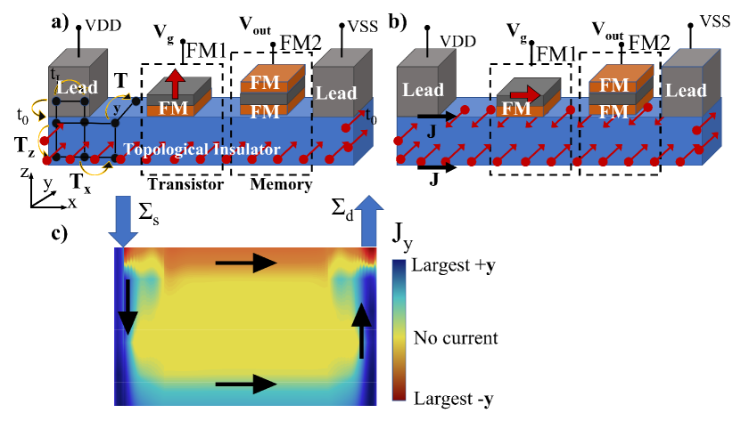
In this paper we present a 1-Transistor 1-magnetic tunnel junction random access memory unit (1T1MTJ-RAM), that can function as a potentially compact, energy efficient building block of a PiM (Fig. 1). The proposed device has two FM/3DTI heterostructures, one functioning as a row-column selector switch, the other as a nonvolatile memory unit. Switching in the second MTJ memory unit (FM2) is based on conventional SOT, with the required spin current at the FM2-3DTI interface provided by the spin momentum locking at the 3DTI surface. The FM that acts as the selector unit (FM1) needs to be electrically switched from out of plane to in plane and back. There are a number of mechanisms to achieve this switching, such as a gated piezoelectric clamped on a magnetostrictive material sitting on the TI Vaz et al. (2015); Trassin (2016); Manchanda et al. (2014); De Ranieri et al. (2013); Verba et al. (2018); Bandyopadhyay et al. (2021), or voltage Controlled Magnetic Anisotropy (VCMA) at the FM/3DTI Manipatruni et al. (2018) to control the polarization of the FM1. Another mechanism is to tune the interface induced anisotropy of a FM/3DTI by changing the free energy of the heterostructure using an applied gate voltage Semenov et al. (2012b); Duan et al. (2015). Although the electrical switching of ferromagnets in FM/3DTI remains challenging, this proposal could encourage more experimental efforts in this direction.
One of the known challenges for the FM1-3DTI is a low On/Off ratio compared to competing CMOS technologies. In this paper we show that as a selector for low power PiM, the On/Off ratio does not need to be very high. In fact, our proposed device is naturally suited for compact PiM designs, as it directly incorporates a selection transistor in the first FM1-3DTI combination. Using an enhanced sense-amplifier for each column with programmable sensing thresholds, it is possible to implement basic Boolean operations (AND, OR, XOR, Majority, and their complements). We describe a possible scheme of building such a PiM towards the end.
I Results
Switching Mechanism The SOT is calculated from the in and out-of plane components of the polarization current applied to the FM2 , obtained by adding phenomenological scattering terms within FM2 of thickness Manchon et al. (2012); Ndiaye et al. (2017); Fischer et al. (2016) on top of the NEGF calculated (Eq. 5a) spin current in the TI
| (1a) | |||||
| (1b) | |||||
where is the Gilbert damping, is the FM magnetization vector, and the net scattering length . are spin relaxation, precessional and decoherence length of the FM, while p is the interface dependent spin transfer efficiency from TI to FM2 (assumed 0.5). Note that due to spin precession in FM2, an out of plane component arises in the SOT, denoted by the imaginary part of .
A gate tunable anisotropy (through strain or VCMA) switches FM1 from out of plane to in plane, which changes the magnetic exchange energy. Note that when the FM1 is in plane, it does not need to be polarized in any specific direction as long as out plane component is negligible. The bandstructure of the 3DTI below FM1 is modified accordingly, shifting locally relative to the Fermi energy (Fig. 2). We shift the bottom surface 0.5 times the top surface under the applied gate voltage , and assume the magnet covers the full TI width laterally. The corresponding NEGF calculated torque with phenomenological corrections (Eq. 1b) is then fed into the Landau-Lifshitz-Gilbert (LLG) equation Slonczewski (1996) self-consistently and quasi-statically, assuming the electron transit speed is orders of magnitude faster than the magnet’s resonant frequency.
The voltage control of the FM1 anisotropy can arise from VCMA effect driven by a vertical electric field across an oxide(MgO)-FM stack, , with VCMA coefficient and oxide thickness and the change in the anisotropy. Alternatively, if we use strain as a switching mechanism for FM1, the applied effective field can be added to as where is the strain coefficient that needs to cancel out the effective anisotropy field . u is the strain direction which needs to be along z (perpendicular to the TI) in this case. For the VCMA mechanism, assuming a thickness of 1 nm for the capped oxide and FM1 layers, a (change in anisotropy volume density) for CoFeB of 1 nm thickness has been reported Kanai et al. (2012); Xue et al. (2019); Rana and Otani (2019a), whereas by doping FM/oxide interface a larger has been achieved as well Rana and Otani (2019b); Nozaki et al. (2019). The effect of oxide on the FM1/3DTI interface is ignored here as it is on the other side of the FM1 (not sandwiched between FM1 and 3DTI), and the effect of the FM1 and FM2 on the bandstructure of the 3DTI is assumed to be limited to the magnetic exchange. For the strain mechanism, of 200-300 has been reported. For both the VCMA and strain, the free energy change from the applied gate can potentially lower the voltage requirements. The required voltage to change the anisotropy of a reliable FM1 with thermal barrier of size nm3 would be 0.3-1 V. Although this is relatively large compared to the applied bias, since there is negligible current in the FM1 heterostructure (we assume a thin insulating buffer), the energy consumption is still small ( 100-300 aJ). Most of the energy consumption comes from the current dissipation in the 3DTI. Using the material parameters reported for room temperature 3DTI switching of ferromagnet DC et al. , the energy consumption from the current in the 3DTI is estimated to be around 10 fJ.
We set up a tight binding Hamiltonian that describes the 3DTI, the Zeeman energy term (magnetic exchange) originating from the FM/3DTI exchange and the on-site energy term from the applied gate voltage at FM1, with parameters fitted to ab-initio calculations (details in the Method section).
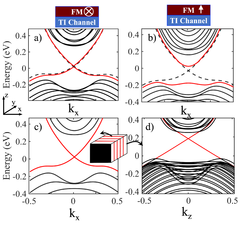
Figs 2a and b show the bandstructure of the 3DTI at the location of the FM1, for the On (magnet in plane of TI) and Off (magnet out of plane) states respectively. For the On state (a), we see a shift in the Dirac point away from the point, relative to the pristine (magnet-free) TI states (Fig. 2c). For the Off state (b) however, the degeneracy is lifted and a corresponding energy gap is created for the top surface states (red solid lines), while at the same time keeping the bottom surface states (dashed lines) intact. We also present the side surface states (Fig.2. d), and as expected (Fig. 1b) they stay gapless for both On and Off states, as the FM only affects part of the top surface. This would mean that for an electrical transistor based on FM/3DTI, the side current would play a crucial role. However, using FM1/TI as a selector as proposed, we avoid dealing with the side current as only the top surface states can apply any appreciable spin orbit torque to FM2.
Reliability For a competitive transistor-memory device based on the FM/3DTI stack, we outline requirements in this paper. The first is the On/Off ratio . For deterministic switching of an in-plane ferromagnet with a given thermal barrier , the critical spin current Sun (2000) with being the effective demagnetization field which we take to be twice . We also need to make sure that when FM1 is out-of-plane in the Off state, the surface leakage current would be small enough to not accidentally switch FM2. The probability of switching FM2 can be approximated using the Fokker-Planck equationLi and Zhang (2004); Butler et al. (2012); Chen et al. (2012)
| (2) | |||||
When the TI is not gapped (FM1 in plane, ), the write error , while when locally gapped (FM1 out of plane, ), the error is . For simplicity we take our target WER in both cases to be identical. For thermally assisted switching (Off) we can solve the Fokker Planck equation, or use the empirical equation . where t is the switching time, and is the spin current overdrive. c is an empirical constant, assumed 1 for in-plane FM2, 2 for out-of-plane, and in between for imperfections.
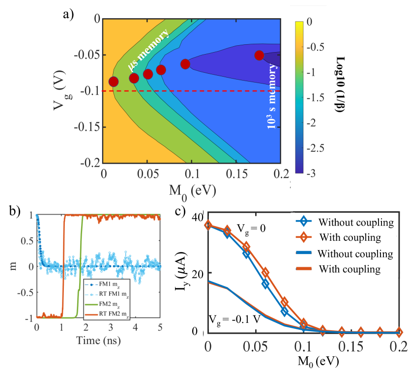
The Zeeman term which breaks time reversal symmetry to open a surface gap must be large enough to allow a small WER for accidental switching. For the Off state, t should be for cache memory and years for long term memory. Eq. I connects WER to material parameters, and Fig. 3.a shows that depending on and , the device can be used in different regimes. For long term storage, we assume , Bedau et al. (2010); Liu et al. (2014) and attempt frequency Breth et al. (2012). When the FM1 is in plane, the required ON is . For short term memory, the off state will need to be to avoid accidentally switching FM2 with the above WER. This means that a modest On/Off ratio of would make the device work. For longer memory applications (hours to days), a larger On/Off ratio (Fig. 3a), is needed. of up to 100 meV has been reported in heterostructureHirahara et al. (2017); Kaveev et al. (2021) which is in the range for up to cache memory.
In Figs. 2c,d we see an energy offset between the TI side and top surface bands, implying different surface conductivities at any given energy. To achieve minimum required magnetic exchange , the applied gate voltage should be approximately equal to the applied bias , VDD. This matches Fig. 3a (VDD eV, VDD eV), where the minimum required for short term (s) memory occurs when is near the midpoint (red dashed line). This implies that without a magnetization, when the chemical potential is tuned to the top or side Dirac point to reduce its conductivity, the other surface will retain a large density of states (DOS), providing a shunting conduction channel between top and bottom. For long term ( s) memory, a higher On/Off ratio is needed which requires a bigger bandgap, hence a larger . Due to the sizable gap opening for long term memory, the critical s for the minimum (red circles) deviate from the midpoint. In Fig. 3c, we performed the simulation with and without any electric coupling between FM1 and 3DTI, which shows that at , the required is only increased by 5-10 percent. At higher , there is no noticeable difference.
Note that the On/Off ratio would be larger if we used a simplified 2D Hamiltonian that only considers surface states. This is because in a realistic TI structure, a significant amount of the current shunts into the bulk of the TI stack, which our 3D geometry naturally takes into account (Fig. 1c). The shunting allows the surface current to go around the gapped region, reducing the On/Off. To have a faster working memory, using a perpendicular ferromagnet as FM2 is preferred, as the switching mechanism would be determined by a field like torque which is faster than an anti-damping torque. However, for a perpendicular ferromagnet an assisting external field is required. This assisting field can originate from the stray field of a capping magnetic layer or the exchange bias of a coupled antiferromagnet-ferromagnet stack Krizakova et al. (2020); Kong et al. (2019); Zheng et al. (2021).
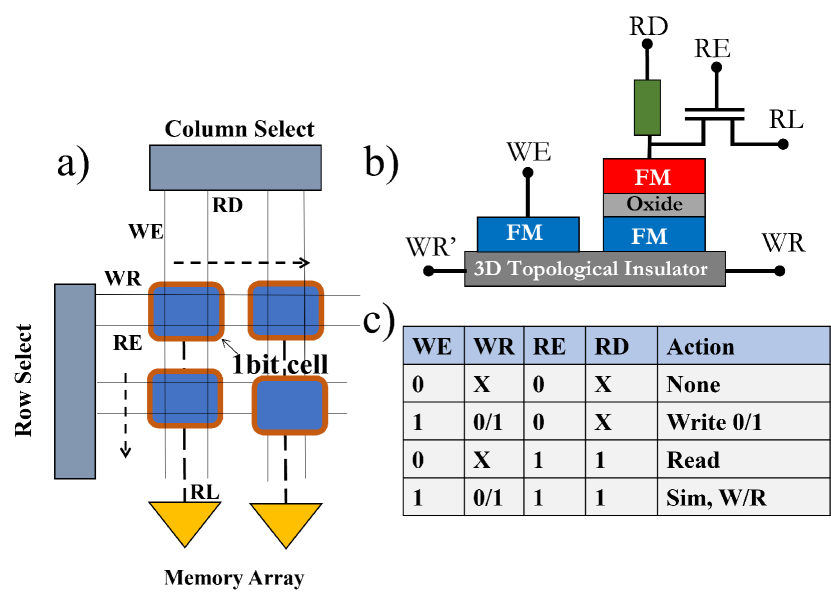
Proposal for a Processor-in-Memory (PiM) design. In Fig. 4a. we show a possible approach for performing in-memory compute functions using an array built out of the presented memory cell. The relation between the voltage lines in Fig. 4 and 1 are as follows: VDD, VSS, Vg, . The cell (Fig. 4b) contains a selection transistor, which acts as a write enable signal. The current flowing in the TI acts as the write signal, with the two ends designated as and . Since a spintronic memory cell requires bipolar currents for programming, we can either use a bipolar current generating selector to drive the signal with grounded, or else reverse the polarities of pairs between and respectively.
The read is performed at the reader MTJ with a voltage divider, which changes the output voltage at the read line (), shared column-wise over the array cells. The reader is charged through the line. We include one transistor in the cell for a read enable functionality () that provides the load resistance for adequate current to the read line per cell depending on the voltage at the divider, critical for the read and PiM functionalities as we describe next. We choose to arrange the read to be done row-wise, whereas the write is done column-wise. This is by no means a necessary condition for designing this architecture, but simply one of the choices we make that allows us the option of simultaneous read and write, if necessary. The read is performed by sensing the current in the read line and comparing with a reference current in the sense amplifier (SA), which then reports the value stored at a specific cell addressed via and signals. The truth table of these operations is shown in Fig. 4c.
The PiM functions are also arranged within the SA over each column. We can build in reference currents that enable Boolean operations over the whole array, by enabling multiple rows at a time. Consider a two-bit operation over any two rows. In this case, the two specific rows are enabled using and all the over the rows are enabled as well. Each of the SA reference currents for the AND operation is set to where is the read current of a cell when it is storing ‘1’. In this case both of the cells being read simultaneously by a single SA will have to be ‘1’ to trigger the SA to report ‘1’, in all other combinations it will report ‘0’. Similarly for the OR case, the reference current can be set as to trigger ‘1’ from SA for even one of the cells being ‘1’. An XOR gate can be implemented by a two threshold SA where the thresholds are and and it is configured to report ‘1’ when reading values in between these two references. The complement functions are easily implemented by using an additional inverter. All these functionalities are built within a single SA and as per the requirements of the computation the SA can be configured to perform a given operation.
Comparison With Existing Technology The in-memory computation is also possible to be performed with existing technologies such as SRAM and DRAM. Note that in order for our proposed device to be competitive, the interface roughness between FM2 and TI must be minimized to have as small as possible (smaller than 0.1). Our proposed device has the lowest energy consumption (Table 1). However, the speed of operation is also lower than the rest, with the energy-delay-product (EDP) being the lowest. For low energy applications, the low energy cost is a higher priority.
| Technology | Energy (fJ) | Latency (ns) |
|---|---|---|
| Proposed device | 10 | 5 |
| SRAM | 50 | 2.7 |
| DRAM | 65 | 3.4 |
| SOT-MRAM | 40 | 2.6 |
II Conclusion
In this article we proposed an in-memory processing device based on the reciprocal interactions in FM-3DTI heterostructures. The main advantage is the integration of the selector-memory units onto a shared transport channel and hence a compact design. Using DFT-calibrated 3D tight binding, NEGF-LLG and Fokker-Planck, we connected the material parameters to switching delay and WER. We showed that a modest ON-OFF suffices for selector action in cache memory, even in presence of current shunting through the sides and bulk. We also showed that as long as the FM1 is not connected to the circuit (no in or out-going current), a modest electric coupling or tunneling between FM1 and 3DTI has only a minor negative effect on the performance. We assumed an in-plane FM2 (type y FM, parallel to spin current polarization) in this work which, to be efficient, needs low damping. This would mean a high-quality interface is crucial. One alternative way is to have FM2 be perpendicular to the spin current polarization, which needs an assisting in-plane magnetic field perpendicular to the spin polarization to break the symmetry. Methods such as adding a second FM layer to use its demagnetization field to act as the assisting magnetic field is shown to work. Other methods, such as structural asymmetry and crystal dependant spin current geometry, have also been proposedShao et al. (2021). To have SOT switching with 3DTI, a type x ferromagnet, inplane polarization but (anti)parallel to the electric currentFukami et al. (2016) should be more efficient than out-plane FM2 as the magnetic exchange between an out-plane FM2 and 3DTI will lower the efficiency of the current generation by the 3DTI. Improvements in the magnetic exchange between FM1 and 3DTI can make even long-term memory applications possible at a low energy cost. Finally, there are experimental challenges in the electrical switching of a ferromagnet in FM/3DTI heterostructures, and further improvements in the voltage controlled switching of ferromagnet methods are needed.
III Methods
In the 3D atomistic grid , the Hamiltonian looks like Liu et al. (2010); Götte et al. (2014); Sengupta et al. (2015); Liu and Hesjedal (2021)
| (3) |
where the onsite energies , and the hopping terms , . For , we use . and are the Pauli matrices in orbital and spin subspaces respectively while is the identity matrix. One layer each of the source and drain is included in the Hamiltonian. The fixed FM in the MTJ is not included in the simulation. Our 3D model allows us to separate the bulk and interfacial components of the charge and current densities (Fig. 1).
We employ the Non-Equilibrium Green’s Function (NEGF) formalism to analyse electron transport and the overall performance of the device. The retarded and correlation Green’s functions are Datta (2012); Ghosh (2016)
| (4) |
with the source/drain Fermi-Dirac distributions. We assume a uniform cross-section that allows us to Fourier transform the transverse y-z hopping terms into . The self-energies are calculated recursively for each and . are the corresponding energy broadening matrices. The spin and charge current densities from site to and SOT torque are calculated as
| (5a) | |||||
| (5b) | |||||
We solve the stochastic LLG equation within a macroscopin model, . is the demagnetization field. The effective anisotropy field , where is the ferromagnet’s thermal stability related to anisotropy , . is the effective field pointing along and directions for FM1 and FM2 respectively at the start of the simulation. For thermal fluctuations we add a stochastic field Vakili et al. , where is a random vector following a normal distribution with zero average. is vacuum permeability, is Boltzmann constant, is temperature, is saturation magnetization, is the electron gyromagnetic ratio, and are volume of FM2 and simulation time step.
Acknowledgments. We acknowledge useful discussions with Patrick Taylor (ARL), Joe Poon, Md Golam Morshed (UVA) and Supriyo Bandyopadhyay (VCU). This work is supported by the Army Research Lab (ARL) and in part by the NSF I/UCRC on Multi-functional Integrated System Technology (MIST) Center; IIP-1439644, IIP-1439680, IIP-1738752, IIP-1939009, IIP-1939050, and IIP-1939012.
References
- Chi et al. (2016) P. Chi, S. Li, C. Xu, T. Zhang, J. Zhao, Y. Liu, Y. Wang, and Y. Xie (ACM/IEEE Annual International Symposium on Computer Architecture (ISCA), USA, 2016) pp. 27–39.
- Ghose et al. (2019) S. Ghose, A. Boroumand, J. S. Kim, J. Gómez-Luna, and O. Mutlu, IBM Journal of Research and Development 63, 3:1 (2019).
- Fong et al. (2016) X. Fong, Y. Kim, K. Yogendra, D. Fan, A. Sengupta, A. Raghunathan, and K. Roy, IEEE Transactions on Computer-Aided Design of Integrated Circuits and Systems 35, 1 (2016).
- Tang et al. (2017) C. Tang, C.-Z. Chang, G. Zhao, Y. Liu, Z. Jiang, C.-X. Liu, M. R. McCartney, D. J. Smith, T. Chen, J. S. Moodera, and J. Shi, Science Advances 3, e1700307 (2017).
- Mellnik et al. (2014) A. R. Mellnik, J. S. Lee, A. Richardella, J. L. Grab, P. J. Mintun, M. H. Fischer, A. Vaezi, A. Manchon, E.-A. Kim, N. Samarth, and D. C. Ralph, Nature 511, 449 (2014).
- Wang et al. (2017) Y. Wang, D. Zhu, Y. Wu, Y. Yang, J. Yu, R. Ramaswamy, R. Mishra, S. Shi, M. Elyasi, K.-L. Teo, Y. Wu, and H. Yang, Nat Commun 8, 1364 (2017).
- Han et al. (2017) J. Han, A. Richardella, S. A. Siddiqui, J. Finley, N. Samarth, and L. Liu, Phys. Rev. Lett. 119, 077702 (2017).
- Han and Liu (2021) J. Han and L. Liu, APL Materials 9, 060901 (2021).
- (9) H. Wu, A. Chen, P. Zhang, H. He, J. Nance, C. Guo, J. Sasaki, T. Shirokura, P. N. Hai, B. Fang, S. A. Razavi, K. Wong, Y. Wen, Y. Ma, G. Yu, G. P. Carman, X. Han, X. Zhang, and K. L. Wang, Nature Communications 12, 6251.
- Semenov et al. (2012a) Y. G. Semenov, X. Duan, and K. W. Kim, Phys. Rev. B 86, 161406 (2012a).
- Taniyama (2015) T. Taniyama, J. Phys.: Condens. Matter 27, 504001 (2015).
- Sajjad and Ghosh (2013) R. Sajjad and A. W. Ghosh, ACS Nano 7, 9808 (2013).
- Wang et al. (2019) K. Wang, M. M. Elahi, L. Wang, K. M. M. Habib, T. Taniguchi, K. Watanabe, J. Hone, A. W. Ghosh, G.-H. Lee, and P. Kim, Proceedings of the National Academy of Sciences 116, 6575 (2019), https://www.pnas.org/doi/pdf/10.1073/pnas.1816119116 .
- Vaz et al. (2015) C. A. F. Vaz, F. J. Walker, C. H. Ahn, and S. Ismail-Beigi, J. Phys.: Condens. Matter 27, 123001 (2015).
- Trassin (2016) M. Trassin, J. Phys.: Condens. Matter 28, 033001 (2016).
- Manchanda et al. (2014) P. Manchanda, U. Singh, S. Adenwalla, A. Kashyap, and R. Skomski, IEEE Transactions on Magnetics 50, 1 (2014).
- De Ranieri et al. (2013) E. De Ranieri, P. E. Roy, D. Fang, E. K. Vehsthedt, A. C. Irvine, D. Heiss, A. Casiraghi, R. P. Campion, B. L. Gallagher, T. Jungwirth, and J. Wunderlich, Nature Mater 12, 808 (2013).
- Verba et al. (2018) R. Verba, I. Lisenkov, I. Krivorotov, V. Tiberkevich, and A. Slavin, Phys. Rev. Applied 9, 064014 (2018).
- Bandyopadhyay et al. (2021) S. Bandyopadhyay, J. Atulasimha, and A. Barman, Applied Physics Reviews 8, 041323 (2021).
- Manipatruni et al. (2018) S. Manipatruni, D. E. Nikonov, C.-C. Lin, B. Prasad, Y.-L. Huang, A. R. Damodaran, Z. Chen, R. Ramesh, and I. A. Young, Science Advances 4, eaat4229 (2018).
- Semenov et al. (2012b) Y. G. Semenov, X. Duan, and K. W. Kim, Phys. Rev. B 86, 161406 (2012b).
- Duan et al. (2015) X. Duan, X.-L. Li, X. Li, Y. G. Semenov, and K. W. Kim, Journal of Applied Physics 118, 224502 (2015).
- Manchon et al. (2012) A. Manchon, R. Matsumoto, H. Jaffres, and J. Grollier, Phys. Rev. B 86, 060404 (2012).
- Ndiaye et al. (2017) P. B. Ndiaye, C. A. Akosa, M. H. Fischer, A. Vaezi, E.-A. Kim, and A. Manchon, Phys. Rev. B 96, 014408 (2017).
- Fischer et al. (2016) M. H. Fischer, A. Vaezi, A. Manchon, and E.-A. Kim, Phys. Rev. B 93, 125303 (2016).
- Slonczewski (1996) J. Slonczewski, Journal of Magnetism and Magnetic Materials 159, L1 (1996).
- Kanai et al. (2012) S. Kanai, M. Yamanouchi, S. Ikeda, Y. Nakatani, F. Matsukura, and H. Ohno, Applied Physics Letters , 122403 (2012).
- Xue et al. (2019) F. Xue, N. Sato, C. Bi, J. Hu, J. He, and S. X. Wang, APL Materials 7, 101112 (2019).
- Rana and Otani (2019a) B. Rana and Y. Otani, Communications Physics 2, 90 (2019a).
- Rana and Otani (2019b) B. Rana and Y. Otani, Communications Physics 2, 90 (2019b).
- Nozaki et al. (2019) T. Nozaki, T. Yamamoto, S. Miwa, M. Tsujikawa, M. Shirai, S. Yuasa, and Y. Suzuki, Micromachines 10, 327 (2019).
- (32) M. DC, R. Grassi, J.-Y. Chen, M. Jamali, D. Reifsnyder Hickey, D. Zhang, Z. Zhao, H. Li, P. Quarterman, Y. Lv, M. Li, A. Manchon, K. A. Mkhoyan, T. Low, and J.-P. Wang, Nature Materials 17, 800.
- Sun (2000) J. Z. Sun, Phys. Rev. B 62, 570 (2000).
- Li and Zhang (2004) Z. Li and S. Zhang, Phys. Rev. B 69, 134416 (2004).
- Butler et al. (2012) W. H. Butler, T. Mewes, C. K. A. Mewes, P. B. Visscher, W. H. Rippard, S. E. Russek, and R. Heindl, IEEE Transactions on Magnetics 48, 4684 (2012).
- Chen et al. (2012) E. Chen, D. Apalkov, A. Driskill-Smith, A. Khvalkovskiy, D. Lottis, K. Moon, V. Nikitin, A. Ong, X. Tang, S. Watts, R. Kawakami, M. Krounbi, S. A. Wolf, S. J. Poon, J. W. Lu, A. W. Ghosh, M. Stan, W. Butler, T. Mewes, S. Gupta, C. K. A. Mewes, P. B. Visscher, and R. A. Lukaszew, IEEE Transactions on Magnetics 48, 3025 (2012).
- (37) J. C. Sankey, Y.-T. Cui, J. Z. Sun, J. C. Slonczewski, R. A. Buhrman, and D. C. Ralph, Nature Physics 4, 67.
- Bedau et al. (2010) D. Bedau, H. Liu, J.-J. Bouzaglou, A. D. Kent, J. Z. Sun, J. A. Katine, E. E. Fullerton, and S. Mangin, Applied Physics Letters 96, 022514 (2010).
- Liu et al. (2014) H. Liu, D. Bedau, J. Sun, S. Mangin, E. Fullerton, J. Katine, and A. Kent, Journal of Magnetism and Magnetic Materials 358-359, 233 (2014).
- Breth et al. (2012) L. Breth, D. Suess, C. Vogler, B. Bergmair, M. Fuger, R. Heer, and H. Brueckl, Journal of Applied Physics 112, 023903 (2012).
- Hirahara et al. (2017) T. Hirahara, S. V. Eremeev, T. Shirasawa, Y. Okuyama, T. Kubo, R. Nakanishi, R. Akiyama, A. Takayama, T. Hajiri, S.-i. Ideta, M. Matsunami, K. Sumida, K. Miyamoto, Y. Takagi, K. Tanaka, T. Okuda, T. Yokoyama, S.-i. Kimura, S. Hasegawa, and E. V. Chulkov, Nano Letters 17, 3493 (2017).
- Kaveev et al. (2021) A. K. Kaveev, S. M. Suturin, V. A. Golyashov, K. A. Kokh, S. V. Eremeev, D. A. Estyunin, A. M. Shikin, A. V. Okotrub, A. N. Lavrov, E. F. Schwier, and O. E. Tereshchenko, Phys. Rev. Materials 5, 124204 (2021).
- Krizakova et al. (2020) V. Krizakova, K. Garello, E. Grimaldi, G. S. Kar, and P. Gambardella, Applied Physics Letters 116, 232406 (2020).
- Kong et al. (2019) W. J. Kong, C. H. Wan, X. Wang, B. S. Tao, L. Huang, C. Fang, C. Y. Guo, Y. Guang, M. Irfan, and X. F. Han, Nat Commun 10, 233 (2019).
- Zheng et al. (2021) Z. Zheng, Y. Zhang, V. Lopez-Dominguez, L. Sánchez-Tejerina, J. Shi, X. Feng, L. Chen, Z. Wang, Z. Zhang, K. Zhang, B. Hong, Y. Xu, Y. Zhang, M. Carpentieri, A. Fert, G. Finocchio, W. Zhao, and P. Khalili Amiri, Nat Commun 12, 4555 (2021).
- Angizi et al. (2019) S. Angizi, Z. He, D. Reis, X. S. Hu, W. Tsai, S. J. Lin, and D. Fan (IEEE Computer Society Annual Symposium on VLSI (ISVLSI), USA, 2019) pp. 197–202.
- Shao et al. (2021) Q. Shao, P. Li, L. Liu, H. Yang, S. Fukami, A. Razavi, H. Wu, K. Wang, F. Freimuth, Y. Mokrousov, M. D. Stiles, S. Emori, A. Hoffmann, J. Åkerman, K. Roy, J.-P. Wang, S.-H. Yang, K. Garello, and W. Zhang, IEEE Transactions on Magnetics 57, 1 (2021).
- Fukami et al. (2016) S. Fukami, T. Anekawa, C. Zhang, and H. Ohno, Nature Nanotechnology 11, 621 (2016).
- Liu et al. (2010) C.-X. Liu, X.-L. Qi, H. Zhang, X. Dai, Z. Fang, and S.-C. Zhang, Phys. Rev. B 82, 045122 (2010).
- Götte et al. (2014) M. Götte, T. Paananen, G. Reiss, and T. Dahm, Phys. Rev. Applied 2, 054010 (2014).
- Sengupta et al. (2015) P. Sengupta, T. Kubis, Y. Tan, and G. Klimeck, Journal of Applied Physics 117, 044304 (2015).
- Liu and Hesjedal (2021) J. Liu and T. Hesjedal, Advanced Materials , 2102427 (2021).
- Datta (2012) S. Datta, Lessons from Nanoelectronics, Lessons from Nanoscience: A Lecture Notes Series, Vol. 2 (World Scientific, USA, 2012).
- Ghosh (2016) A. Ghosh, Nanoelectronics A Molecular View, World Scientific Series in Nanoscience and Nanotechnology No. Volume 13 (World Scientific, USA, 2016).
- (55) H. Vakili, Y. Xie, S. Ganguly, and A. W. Ghosh, 2021, 2110.02641, arXiv, http://arxiv.org/abs/2110.02641 Nov 19 2021.