Atomic Layer Epitaxy of Kagome Magnet Fe3Sn2 and Sn-modulated Heterostructures
Abstract
Magnetic materials with kagome crystal structure exhibit rich physics such as frustrated magnetism, skyrmion formation, topological flat bands, and Dirac/Weyl points. Until recently, most studies on kagome magnets have been performed on bulk crystals or polycrystalline films. Here we report the atomic layer molecular beam epitaxy synthesis of high-quality thin films of topological kagome magnet Fe3Sn2. Structural and magnetic characterization of Fe3Sn2 on epitaxial Pt(111) identifies highly ordered films with c-plane orientation and an in-plane magnetic easy axis. Studies of the local magnetic structure by anomalous Nernst effect imaging reveals in-plane oriented micrometer size domains. Superlattice structures consisting of Fe3Sn2 and Fe3Sn are also synthesized by atomic layer molecular beam epitaxy, demonstrating the ability to modulate the sample structure at the atomic level. The realization of high-quality films by atomic layer molecular beam epitaxy opens the door to explore the rich physics of this system and investigate novel spintronic phenomena by interfacing Fe3Sn2 with other materials.
In recent years, studies on magnetic topological materials with kagome lattices have become one of the hottest frontiers of condensed matter research, due to their exotic physical properties in both real space and momentum space [1, 2]. In momentum space, angle-resolved photoemission spectroscopy (ARPES) experiments on Mn3Sn, Fe3Sn2, FeSn, and CoSn [3, 4, 5, 6] show that kagome lattices give rise to Dirac cones and flat bands which are topologically protected and are of particular interest. In addition, scanning tunneling spectroscopy finds evidence for topological flat bands as a sharp peak in the local density of states [7]. These topologically nontrivial features result in signatures of anomalous transport (e.g. chiral anomaly) in magnetotransport experiments [3, 8]. Furthermore, it is theoretically predicted that the band structures of the kagome topological magnets can be controlled by tuning of their magnetic structures [3, 1]. In real space, the kagome topological magnets have layered structures with spins occupying corner-sharing triangular lattices, which leads to geometrical spin frustration [9, 10]. A surprisingly large anomalous Hall effect (AHE) and magneto-optic Kerr effect (MOKE) have been reported in noncollinear antiferromagnet Mn3Sn, even with vanishingly small net magnetization [10, 11]. Skymrmion spin textures have been observed in ferromagnetic Fe3Sn2 resulting from the competition of exchange, dipolar, and Zeeman energies [12, 13]. However, most of the studies on the kagome magnets have been done on bulk materials [9, 14, 10, 15, 12, 4, 11, 13, 5] with a few papers reporting the growth and characterization of epitaxial films [16, 17, 18, 19, 20]. Looking forward, the heterostructures consisting of kagome magnets will be interesting for both fundamental research and applications, due to the possibility of tuning the magnetic and topological properties via interface interactions, epitaxial strain, and quantum confinement. However, all the reported studies on epitaxial Fe3Sn2 thin films have been focusing on high temperature growth so far, which may not allow for the formation of well-defined heterostructures due to interdiffusion at elevated temperatures. Therefore, lower temperature growth of Fe3Sn2 is desired for the future development of heterostructures and superlattices based on kagome magnets.
In this paper, we report the atomic layer molecular beam epitaxy (AL-MBE) growth of high-quality Fe3Sn2 thin films on Pt(111)/Al2O3(0001) substrates at lower temperatures. By sequentially depositing Fe3Sn kagome layers and Sn2 layers (see Figure 1a), we are able to control the sample structure at the atomic level. The crystalline structure of our Fe3Sn2 sample is confirmed by a combination of in situ reflection high energy electron diffraction (RHEED), X-ray diffraction (XRD) and transmission electron microscopy (TEM). Energy-dispersive X-ray spectroscopy (EDX) shows sharp interfaces for low temperature growth. The magnetic properties of Fe3Sn2 are investigated using MOKE, superconducting quantum interference device (SQUID) and anomalous Nernst effect (ANE). Using a microscopy technique based on ANE, we successfully image the in-plane oriented domain structure of the epitaxial Fe3Sn2 films and investigate the magnetization reversal as a function of applied field. We further utilize AL-MBE to precisely control the stacking sequences of Fe3Sn and Sn2 atomic layers, making superlattices with modulation of Sn2 layers and confirm their structures by TEM and EDX. This demonstrates the potential of using AL-MBE to generate designer materials consisting of kagome layers (Mn3Sn, Fe3Sn, Co3Sn, etc.) and Sn2 spacer layers with precision control of sample structures at the atomic level.

Fe3Sn2 is a ferromagnet with a high Curie temperature, = 670 K [21], and saturation magnetization of 1.9 per Fe at low temperature [4]. Fig. 1a shows the crystal structure of Fe3Sn2 (space group Rm, with lattice constants a = 5.338 Å and c = 19.789 Å [21]) which consists of Fe3Sn kagome layers and Sn2 spacer layers. In each Fe3Sn monolayer, the Fe atoms form corner-sharing equilateral triangles surrounding hexagons, with Sn atoms sitting in the center of the hexagons. The alternating sequence of one Sn2 monolayer with honeycomb lattice and two Fe3Sn kagome layers produces the layered crystal structure of Fe3Sn2.
Based on this layered structure, we synthesized Fe3Sn2 thin films on top of epitaxial Pt(111) buffer layers on Al2O3(0001) substates by AL-MBE. The epitaxial growth was performed in an MBE chamber with a base pressure of Torr. Films were deposited on Al2O3(0001) substrates (MTI Corporation) prepared by annealing in air at 1000 ∘C for 3 hours followed by annealing in ultrahigh vacuum (UHV) at 500 ∘C for 30 minutes. A 5 nm Pt(111) buffer layer was deposited from an e-beam evaporator (Pt: 99.99%, Kurt J. Lesker) onto the Al2O3 (0001) substrate by growing the first 0.6 nm at 440 ∘C and the rest 4.4 nm while cooling down from 140 ∘C to 80 ∘C. The Pt buffer layer was post-annealed at 300 ∘C to improve the crystallinity and surface roughness. The Fe3Sn2 layer was grown on Pt(111) at 100 ∘C using the following AL-MBE sequence: deposit two atomic layers of Fe3Sn with a Fe:Sn flux ratio of 3:1, deposit one atomic layer of Sn2 with the growth time same as two Fe3Sn layers, then repeat. The Fe and Sn fluxes were generated from Knudsen cells (Fe: 99.99%, Alfa Aesar; Sn: 99.998%, Alfa Aesar) and the growth rates were determined using a quartz deposition monitor that was calibrated by x-ray reflectometry. Typical growth rates were 0.85 Å/min, 0.67 Å/min, and 0.45 Å/min for Fe, Sn, and Pt, respectively. To protect the sample from oxidation, a 5 nm CaF2 capping layer was deposited on top of the Fe3Sn2.
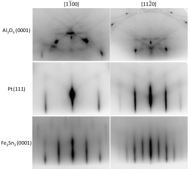
RHEED patterns were measured during growth to characterize the epitaxial growth and determine the in-plane lattice constants. Figure 1b shows the RHEED patterns for the Al2O3(0001) substrate (top row), 5 nm Pt buffer layer (middle row), and the Fe3Sn2 layer after 20 nm of growth (bottom row). The left and right columns show patterns taken for the beam along the and directions of the substrate, respectively. With in-plane rotation of the sample, RHEED exhibits the same pattern every 60∘ (i.e. six-fold rotation symmetry) with the patterns alternating between -type and -type every 30∘. For the in-plane epitaxial alignment, the Pt(111) and Fe3Sn2(0001) surface unit cells are aligned with each other and rotated 30∘ with respect to the Al2O3(0001) substrate, as (bulk values for in-plane lattice constant are Å, Å, Å).
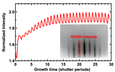
The streaky patterns observed during Fe3Sn2 growth signify diffraction from a two-dimensional surface. In addition, we observe oscillations (Fig. 1c) in the normalized RHEED intensity where the maxima occurs for the Fe3Sn termination and the minima occurs for the Sn2 termination. The normalization is performed by dividing the intensity of the background and is helpful for canceling variations in the incident beam intensity and background lighting. Except for the change in RHEED intensity, we did not observe any other significant differences in the RHEED pattern between Sn2 and Fe3Sn terminations. Nevertheless, the presence of RHEED oscillations in atomic layer MBE confirms the modulation of the surface termination during growth.
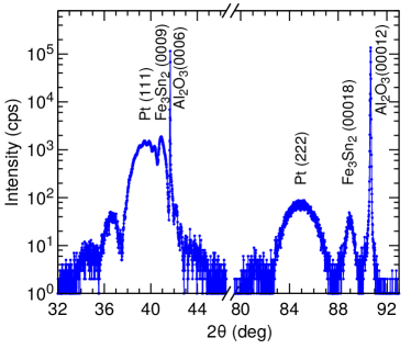
Films grown by this method were studied with XRD using Cu K- line (wavelength 1.5406 Å) to analyze their crystal structure. A representative - scan of a 20 nm film grown at 100 ∘C is shown in Figure 2a and includes the Fe3Sn2 (0009) peak with several Laue oscillations, indicating a smooth film. The out-of-plane lattice parameter extracted from analysis of this scan is 19.85 Å which agrees well with previous reports of 19.789 Å [21]. A peak from the 5 nm Pt(111) buffer also shows Laue oscillations with larger angular period due to smaller thickness of the Pt layer in comparison with Fe3Sn2 layer (Pt Laue peaks at 34.5∘, 36.7∘, and 43.5∘) demonstrating high quality of the buffer layer. At larger angles we observe Fe3Sn2 (00018) and Pt(222) peaks, with no additional peaks that could be attributed to impurity phases (see Supplementary Material (SM) sections 2 for full range scans).
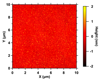
To characterize the surface topography of the sample, we performed atomic force microscope (AFM) measurements on uncapped 20 nm Fe3Sn2 films. Figure 2b shows a typical 10 m 10 m scan of a 20 nm Fe3Sn2 sample grown at 100 ∘C. The AFM image indicates that the sample has flat surface, with root-mean-square (rms) roughness of 0.362 nm.
An important factor for material synthesis is the growth temperature. To optimize the growth temperature, we performed AFM and XRD measurements on a series of samples grown at different temperatures ranging from room temperature to 200 ∘C. The AFM and XRD results are shown in SM sections 1 and 2, respectively. We conclude that 100 ∘C is the optimized growth temperature as it gives the best AFM roughness and sharp XRD peaks.
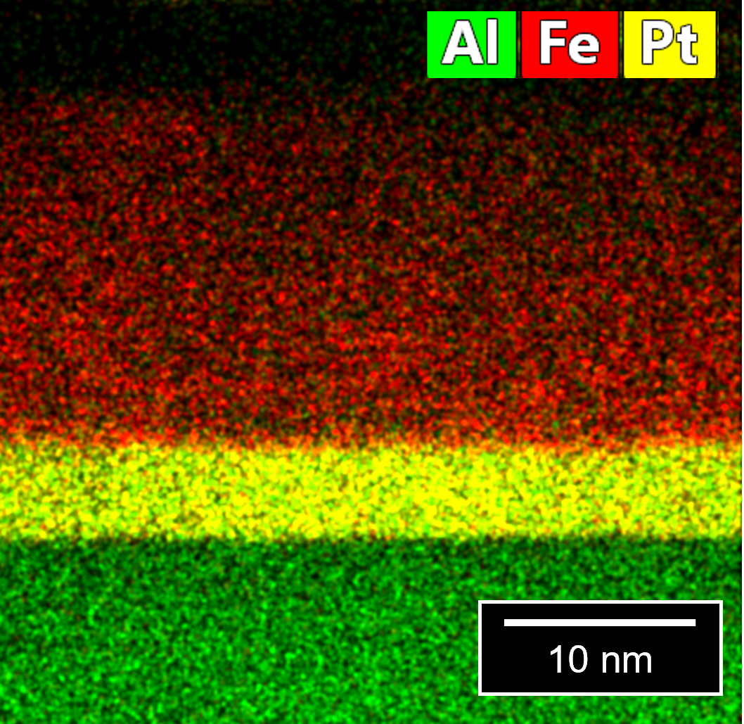
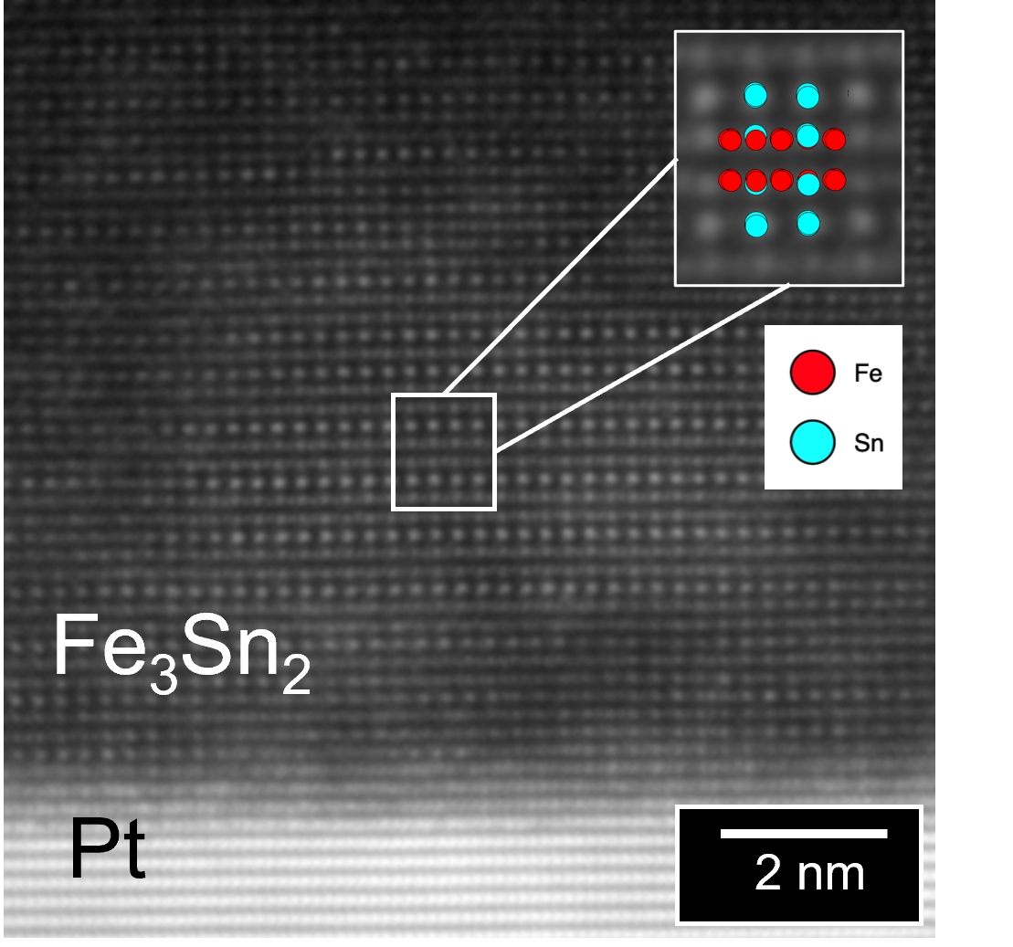
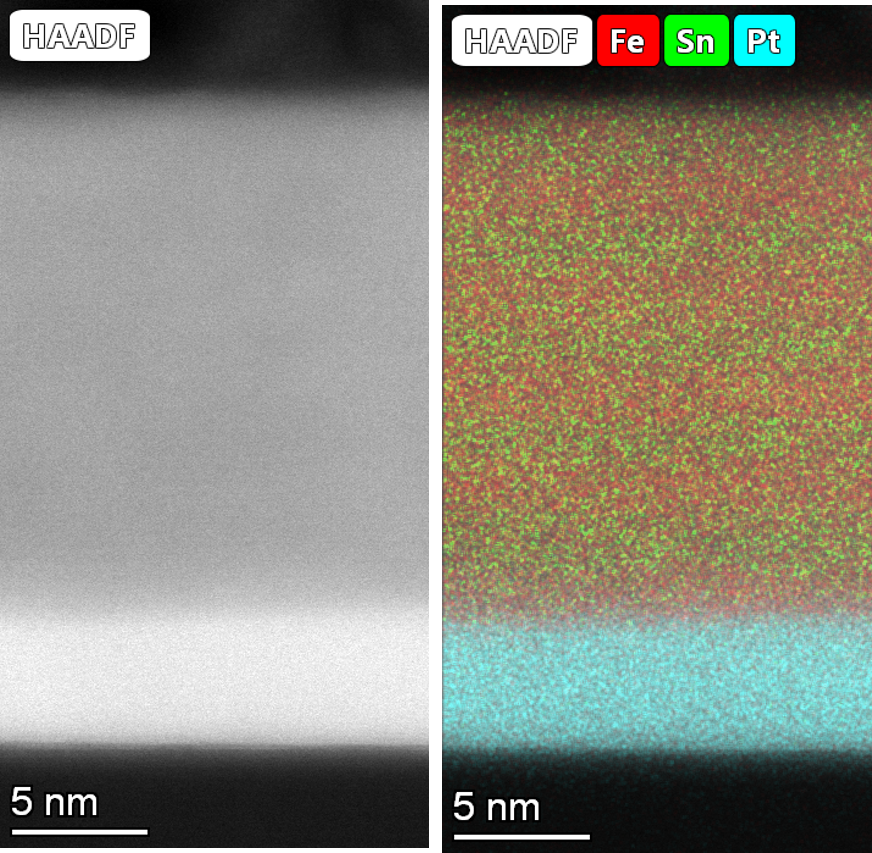
The epitaxial quality of the 20 nm Fe3Sn2 sample grown at 100 ∘C was examined using a probe-corrected Themis Z S/TEM at 200 kV. Figures 2c and 2d show the energy-dispersive x-ray (EDX) chemical map and cross-sectional scanning transmission electron microscopy (STEM) image, revealing a clear interface between the Pt buffer and Fe3Sn2 thin film. The stoichiometry of Fe3Sn2 thin films was confirmed by electron energy loss spectroscopy (EELS), which gives an atomic ratio of Fe:Sn 1.5 (see SM sections 3 for details). To identify the crystalline quality of the Fe3Sn2 thin films, atomic resolution high-angle annular dark-field (HAADF) STEM images of the Fe3Sn2/Pt interface were acquired along the Fe3Sn2 [110] direction (see Figure 2d). Since the contrast in HAADF STEM is approximately proportional to the square of the atomic number, the Sn atoms in the Sn2 atomic layers appear as the brightest spots, while the atoms in Fe3Sn kagome layers are dimmer (the atomic numbers of Sn and Fe are 50 and 26, respectively). The alternating sequence of one Sn2 monolayer and two Fe3Sn kagome layers shows a highly crystalline film with the expected Fe3Sn2 phase, although some stacking faults are observed.
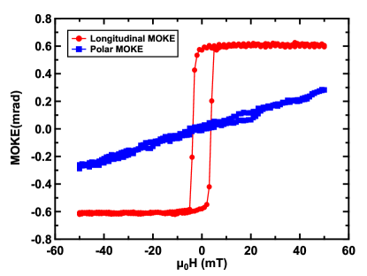
To investigate the in-plane and out-of-plane magnetic properties of the Fe3Sn2 films, we measured longitudinal and polar MOKE hysteresis loops. The samples were probed using a linearly-polarized He-Ne laser (633 nm wavelength, W power, m spot size) and a polarizing beamsplitter, photodiode bridge, and lock-in amplifier (463 Hz intensity modulation) to detect the Kerr rotation. The laser beam had a 45∘ angle of incidence for longitudinal MOKE and normal incidence for polar MOKE. Figure 3a shows a representative longitudinal hysteresis loop (red curve) measured on a 20 nm thick Fe3Sn2 sample. The square hysteresis loop with a coercivity of 2.4 mT indicates ferromagnetic order with in-plane magnetization. In contrast, the polar hysteresis loop (blue curve) shows a small Kerr rotation with slight variation with out-of-plane magnetic field. We repeated the longitudinal MOKE measurements on additional samples with thicknesses varying from 5 nm to 20 nm. The coercive fields of the samples are between 3.0 mT and 4.2 mT (SM section 4). Together, the longitudinal and polar MOKE loops show that the Fe3Sn2 samples have an easy-plane magnetic anisotropy. This agrees with previous studies of Fe3Sn2 films grown by sputter deposition [19] and in bulk crystals thinned to below 100 nm [22].
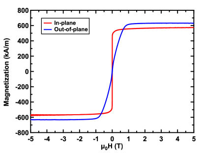
We also performed SQUID magnetometry measurements on our Fe3Sn2 films. Figure 3b shows hysteresis loops of a 20 nm thick Fe3Sn2 sample measured with in-plane (red curve) and out-of-plane (blue curve) magnetic fields. The in-plane hysteresis loop exhibits a sharp switching behavior while the out-of-plane hysteresis loop exhibits almost linear behavior within 1 Tesla and saturates at 1 Tesla, suggesting that our Fe3Sn2 samples have easy-plane anisotropy. Furthermore, our SQUID results give a saturation magnetization = 630 kA/m, which is consistent with previous studies [19, 23].
The magnetic domain structures of Fe3Sn2 films are of interest due to the observation of skyrmions in bulk Fe3Sn2, but has not yet been studied in thin films. Longitudinal MOKE microscopy with oblique angle incidence can detect the in-plane magnetization and therefore determine in-plane domain structure of our Fe3Sn2 films. However, in this manuscript, we choose to use thermal gradient microscopy (TGM) [24, 25, 26] over longitudinal MOKE to image domain structure because we found that it has a better signal-to-noise ratio in our experimental setup.
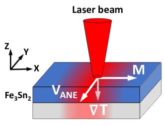
TGM is based on moving a laser spot over the sample surface, and recording a voltage induced by the local laser heating. The thermal gradient generated in the out-of-plane direction and a component of magnetization in the direction give rise to the anomalous Nernst effect, which is detected as a voltage along the direction, (see Fig. 4a).
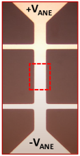
For the ANE imaging, we fabricated 10 m wide Hall bar devices by a combination of photolithography and argon ion milling (Fig. 4b). The laser excitation for the thermal gradient was produced by a frequency-doubled (BaB2O4 crystal) mode-locked Ti:Sapphire laser for a wavelength of 400 nm. The laser beam with 0.7 mW power was focused by a 50 objective lens (NA of 0.6) to a spot size of 0.9 m, and a fast steering mirror in the 4f alignment scheme was used for scanning the laser spot over the sample surface. The intensity of the beam was modulated at a frequency of 120 kHz and the generated ANE voltage was detected using a lock-in amplifier.
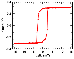
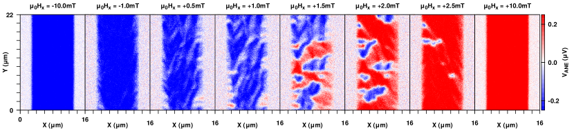
We first utilized the ANE microscope to measure a detailed hysteresis loop at a fixed position. As shown in Fig. 4c for magnetic field along the direction, the hysteresis loop shows a gradual reversal followed by magnetization switching with coercivity of 2.3 mT. This has a similar coercivity but more gradual initial reversal than the in-plane hysteresis loops obtained by MOKE (Fig. 3a). The origin of the different hysteresis properties is revealed by imaging the magnetic domain structure of Fe3Sn2 films at a series of magnetic fields. A representative sequence during the magnetization reversal is shown in Fig. 4d. Starting at -10.0 mT, the magnetization is in a saturated state along (blue). The reversal initiates with the nucleation of white regions with , mainly at the edges of the sample. This can be explained by the minimization of domain wall energy as the edge boundary does not contribute a domain wall energy cost. The nucleation at the edges initiates magnetization reversal which results in a more rounded hysteresis loop compared to the uniform films. With increasing magnetic field, domains of opposite polarity grow inward and coalesce across the channel. At about +1.5 mT, the magnetic structure is in a multidomain state with characteristic features (e.g. blue and red regions) ranging from 1 to 10 microns in size. By +2.5 mT, most of the magnetic moments have switched to direction, with only a few regions remaining along . Finally, at +10.0 mT the magnetization reversal is complete and the films is fully saturated along .
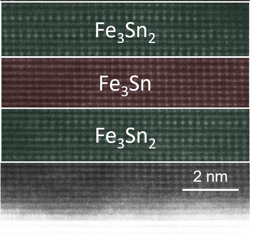
Finally, to demonstrate the ability to control the sample structure at the atomic level, we synthesized a [Fe3Sn2 (2 nm)/Fe3Sn (2 nm)]5 superlattice using the AL-MBE technique. The [Fe3Sn2/Fe3Sn]5 superlattice samples were grown under the same conditions as Fe3Sn2 samples but with different atomic layer deposition sequences. For a 2 nm Fe3Sn layer, we deposit nine atomic layers of Fe3Sn without any Sn2 spacers. For a 2 nm Fe3Sn2 layer, we deposit two atomic layers of Fe3Sn, and one atomic layer of Sn2 and repeat a total of three times. The RHEED pattern of a [Fe3Sn2/Fe3Sn]5 superlattice along the direction of c-sapphire is shown in Figure 5a.
Such control of the stacking sequence with atomic level precision is confirmed by the HAADF STEM image of the [Fe3Sn2/Fe3Sn] superlattice structure in Figure 5b. From the STEM image, an alternating sequence of 2 nm Fe3Sn2 (false colored in green) and 2 nm Fe3Sn (false colored in red) can be observed with atomic resolution. Within 2 nm Fe3Sn2 layer, a repetitive stacking of two Fe3Sn atomic layers and one Sn2 atomic layer can be observed. In contrast, we can only see Fe3Sn atomic layers in 2 nm Fe3Sn layer. The STEM-EDX chemical map further reveals the repetition of the [Fe3Sn2/Fe3Sn]5 superlattice structure along the growth direction as shown in Figure 5c, where a 2 nm Fe3Sn2 layer has a stronger signal for the Sn element compared to a 2 nm Fe3Sn layer.
In conclusion, we report the atomic layer epitaxy growth of kagome ferromagnet Fe3Sn2 thin films on Pt(111)/Al2O3(0001) at low temperatures. The high quality of epitaxial Fe3Sn2 films is confirmed by in situ RHEED, XRD, AFM and TEM. Low temperature growth helps to generate a sharp interface between Fe3Sn2 and Pt layers, which has been observed by EDX. The magnetic properties are investigated by magneto-optical Kerr effect, SQUID magnetometry, and anomalous Nernst effect, confirming the easy-plane magnetic anisotropy of the thin films. Using ANE microscopy, we successfully resolve the local in-plane oriented micrometer size domains during magnetization reversal. Finally, we demonstrate the ability to control the sample structure at the atomic level by synthesizing [Fe3Sn2/Fe3Sn]5 superlattices and confirming their structure by TEM. These advances enable novel heterostructures for exploring the rich physics of kagome magnets.
Acknowledgements
S.C., B.W., I.L., N.B., D.W.M and R.K.K. acknowledge support from DARPA Grant No. D18AP00008. A.J.B. and R.K.K. acknowledge support from AFOSR MURI 2D MAGIC Grant No. FA9550-19-1-0390 and DOE Grant No. DE-SC0016379. B.W. also thanks the support from Presidential Fellowship of the Ohio State University. This research was partially supported by the Center for Emergent Materials, an NSF MRSEC, under award number DMR-2011876. Electron microscopy experiments were supported by the Center for Electron Microscopy and Analysis at the Ohio State University.
Author contributions
S.C., I.L., and R.K.K. conceived the experiments. S.C. conducted the MBE growth, AFM measurements, MOKE measurements and SQUID measurements. I.L. conducted the ANE measurements. A.J.B. and I.L. conducted the XRD measurements. B.W., N.B., and D.W.M. conducted the TEM measurements. All authors participated in data analysis and preparation of the manuscript.
References
- Šmejkal et al. [2018] L. Šmejkal, Y. Mokrousov, B. Yan, and A. H. MacDonald, Topological antiferromagnetic spintronics, Nature Physics 14, 242 (2018).
- Yang et al. [2017] H. Yang, Y. Sun, Y. Zhang, W.-J. Shi, S. S. Parkin, and B. Yan, Topological weyl semimetals in the chiral antiferromagnetic materials Mn3Ge and Mn3Sn, New Journal of Physics 19, 015008 (2017).
- Kuroda et al. [2017] K. Kuroda, T. Tomita, M.-T. Suzuki, C. Bareille, A. A. Nugroho, P. Goswami, M. Ochi, M. Ikhlas, M. Nakayama, S. Akebi, R. Noguchi, R. Ishii, N. Inami, K. Ono, H. Kumigashira, A. Varykhalov, T. Muro, T. Koretsune, R. Arita, S. Shin, T. Kondo, and S. Nakatsuji, Evidence for magnetic Weyl fermions in a correlated metal, Nature Materials 16, 1090 (2017).
- Ye et al. [2018] L. Ye, M. Kang, J. Liu, F. von Cube, C. R. Wicker, T. Suzuki, C. Jozwiak, A. Bostwick, E. Rotenberg, D. C. Bell, L. Fu, R. Comin, and J. G. Checkelsky, Massive Dirac fermions in a ferromagnetic kagome metal, Nature 555, 638 (2018).
- Kang et al. [2020a] M. Kang, L. Ye, S. Fang, J.-S. You, A. Levitan, M. Han, J. I. Facio, C. Jozwiak, A. Bostwick, E. Rotenberg, M. K. Chan, R. D. McDonald, D. Graf, K. Kaznatcheev, E. Vescovo, D. C. Bell, E. Kaxiras, J. van den Brink, M. Richter, M. Prasad Ghimire, J. G. Checkelsky, and R. Comin, Dirac fermions and flat bands in the ideal kagome metal FeSn, Nature Materials 19, 163 (2020a).
- Kang et al. [2020b] M. Kang, S. Fang, L. Ye, H. C. Po, J. Denlinger, C. Jozwiak, A. Bostwick, E. Rotenberg, E. Kaxiras, J. G. Checkelsky, and R. Comin, Topological flat bands in frustrated kagome lattice CoSn, Nature Communications 11, 4004 (2020b).
- Yin et al. [2019] J.-X. Yin, S. S. Zhang, G. Chang, Q. Wang, S. S. Tsirkin, Z. Guguchia, B. Lian, H. Zhou, K. Jiang, I. Belopolski, N. Shumiya, D. Multer, M. Litskevich, T. A. Cochran, H. Lin, Z. Wang, T. Neupert, S. Jia, H. Lei, and M. Z. Hasan, Negative flat band magnetism in a spin–orbit-coupled correlated kagome magnet, Nature Physics 15, 443 (2019).
- Chen et al. [2021] T. Chen, T. Tomita, S. Minami, M. Fu, T. Koretsune, M. Kitatani, I. Muhammad, D. Nishio-Hamane, R. Ishii, F. Ishii, R. Arita, and S. Nakatsuji, Anomalous transport due to Weyl fermions in the chiral antiferromagnets Mn3X, X = Sn, Ge, Nature Communications 12, 572 (2021).
- Fenner et al. [2009] L. Fenner, A. Dee, and A. Wills, Non-collinearity and spin frustration in the itinerant kagome ferromagnet Fe3Sn2, Journal of Physics: Condensed Matter 21, 452202 (2009).
- Nakatsuji et al. [2015] S. Nakatsuji, N. Kiyohara, and T. Higo, Large anomalous Hall effect in a non-collinear antiferromagnet at room temperature, Nature 527, 212 (2015).
- Higo et al. [2018] T. Higo, H. Man, D. B. Gopman, L. Wu, T. Koretsune, O. M. J. van ’t Erve, Y. P. Kabanov, D. Rees, Y. Li, M.-T. Suzuki, S. Patankar, M. Ikhlas, C. L. Chien, R. Arita, R. D. Shull, J. Orenstein, and S. Nakatsuji, Large magneto-optical Kerr effect and imaging of magnetic octupole domains in an antiferromagnetic metal, Nature Photonics 12, 73 (2018).
- Hou et al. [2017] Z. Hou, W. Ren, B. Ding, G. Xu, Y. Wang, B. Yang, Q. Zhang, Y. Zhang, E. Liu, F. Xu, W. Wang, G. Wu, X. Zhang, B. Shen, and Z. Zhang, Observation of Various and Spontaneous Magnetic Skyrmionic Bubbles at Room Temperature in a Frustrated Kagome Magnet with Uniaxial Magnetic Anisotropy, Advanced Materials 29, 1701144 (2017).
- Hou et al. [2019] Z. Hou, Q. Zhang, G. Xu, S. Zhang, C. Gong, B. Ding, H. Li, F. Xu, Y. Yao, E. Liu, G. Wu, X.-x. Zhang, and W. Wang, Manipulating the Topology of Nanoscale Skyrmion Bubbles by Spatially Geometric Confinement, ACS Nano 13, 922 (2019).
- Kida et al. [2011a] T. Kida, L. A. Fenner, A. A. Dee, I. Terasaki, M. Hagiwara, and A. S. Wills, The giant anomalous Hall effect in the ferromagnet Fe3Sn2—a frustrated kagome metal, J. Phys.: Condens. Matter 23, 112205 (2011a).
- Nayak et al. [2016] A. K. Nayak, J. E. Fischer, Y. Sun, B. Yan, J. Karel, A. C. Komarek, C. Shekhar, N. Kumar, W. Schnelle, J. Kübler, C. Felser, and S. S. P. Parkin, Large anomalous Hall effect driven by a nonvanishing Berry curvature in the noncolinear antiferromagnet Mn3Ge, Science Advances 2, e1501870 (2016).
- Markou et al. [2018] A. Markou, J. M. Taylor, A. Kalache, P. Werner, S. S. P. Parkin, and C. Felser, Noncollinear antiferromagnetic Mn3Sn films, Phys. Rev. Materials 2, 051001 (2018).
- Inoue et al. [2019] H. Inoue, M. Han, L. Ye, T. Suzuki, and J. G. Checkelsky, Molecular beam epitaxy growth of antiferromagnetic Kagome metal FeSn, Appl. Phys. Lett. 115, 072403 (2019).
- Taylor et al. [2020] J. M. Taylor, A. Markou, E. Lesne, P. K. Sivakumar, C. Luo, F. Radu, P. Werner, C. Felser, and S. S. P. Parkin, Anomalous and topological Hall effects in epitaxial thin films of the noncollinear antiferromagnet Mn3Sn, Phys. Rev. B 101, 094404 (2020).
- Khadka et al. [2020] D. Khadka, T. R. Thapaliya, S. Hurtado Parra, J. Wen, R. Need, J. M. Kikkawa, and S. X. Huang, Anomalous Hall and Nernst effects in epitaxial films of topological kagome magnet Fe3Sn2, Phys. Rev. Materials 4, 084203 (2020).
- Hong et al. [2020] D. Hong, C. Liu, H.-W. Hsiao, D. Jin, J. E. Pearson, J.-M. Zuo, and A. Bhattacharya, Molecular beam epitaxy of the magnetic kagome metal FeSn on LaAlO3(111), AIP Advances 10, 105017 (2020).
- Giefers and Nicol [2006] H. Giefers and M. Nicol, High pressure X-ray diffraction study of all Fe–Sn intermetallic compounds and one Fe–Sn solid solution, Journal of Alloys and Compounds 422, 132 (2006).
- Wang et al. [2021] B. Wang, P.-k. Wu, N. Bagués Salguero, Q. Zheng, J. Yan, M. Randeria, and D. W. McComb, Stimulated nucleation of skyrmions in a centrosymmetric magnet, ACS nano 15, 13495 (2021).
- Kida et al. [2011b] T. Kida, L. Fenner, A. Dee, I. Terasaki, M. Hagiwara, and A. Wills, The giant anomalous hall effect in the ferromagnet Fe3Sn2—a frustrated kagome metal, Journal of Physics: Condensed Matter 23, 112205 (2011b).
- Weiler et al. [2012] M. Weiler, M. Althammer, F. D. Czeschka, H. Huebl, M. S. Wagner, M. Opel, I.-M. Imort, G. Reiss, A. Thomas, R. Gross, and S. T. B. Goennenwein, Local Charge and Spin Currents in Magnetothermal Landscapes, Phys. Rev. Lett. 108, 106602 (2012).
- Gray et al. [2019] I. Gray, T. Moriyama, N. Sivadas, G. M. Stiehl, J. T. Heron, R. Need, B. J. Kirby, D. H. Low, K. C. Nowack, D. G. Schlom, D. C. Ralph, T. Ono, and G. D. Fuchs, Spin Seebeck Imaging of Spin-Torque Switching in Antiferromagnetic Pt/NiO Heterostructures, Phys. Rev. X 9, 041016 (2019).
- Reichlova et al. [2019] H. Reichlova, T. Janda, J. Godinho, A. Markou, D. Kriegner, R. Schlitz, J. Zelezny, Z. Soban, M. Bejarano, H. Schultheiss, P. Nemec, T. Jungwirth, C. Felser, J. Wunderlich, and S. T. B. Goennenwein, Imaging and writing magnetic domains in the non-collinear antiferromagnet Mn3Sn, Nature Communications 10, 5459 (2019).