Experimental observation of ABCB stacked tetralayer graphene
Abstract
In tetralayer graphene, three inequivalent layer stackings should exist, however, only rhombohedral (ABCA) and Bernal (ABAB) stacking have so far been observed. The three stacking sequences differ in their electronic structure, with the elusive third stacking (ABCB) being unique as it is predicted to exhibit an intrinsic bandgap as well as locally flat bands around the K points. Here, we use scattering-type scanning near-field optical microscopy and confocal Raman microscopy to identify and characterize domains of ABCB stacked tetralayer graphene. We differentiate between the three stacking sequences by addressing characteristic interband contributions in the optical conductivity between 0.28 and 0.56 eV with amplitude and phase-resolved near-field nano-spectroscopy. By normalizing adjacent flakes to each other, we achieve good agreement between theory and experiment, allowing for the unambiguous assignment of ABCB domains in tetralayer graphene. These results establish near-field spectroscopy at the interband transitions as a semi-quantitative tool, enabling the recognition of ABCB domains in tetralyer graphene flakes and therefore, providing a basis to study correlation physics of this exciting new phase.
otherfnsymbols ††‡‡§§¶¶ \alsoaffiliationPeter Grünberg Institute (PGI-9), Forschungszentrum Jülich, 52425 Jülich, Germany \alsoaffiliationPeter Grünberg Institute (PGI-9), Forschungszentrum Jülich, 52425 Jülich, Germany \alsoaffiliationMax Planck Institute for the Structure and Dynamics of Matter, Center for Free Electron Laser Science, Hamburg, Germany
The crystallographic stacking order of few layer graphene (FLG) greatly influences its electronic and optical properties. Naturally occurring crystallographic structures of graphene host interesting phenomena such as quantum Hall states in single and bilayer graphene 1, 2, with Bernal stacked bilayer graphene exhibiting superconductivity upon applying a magnetic field 3. Half- and quarter-metals have been reported for rhombohedral stacked trilayer graphene 4, 5, while a charge-transfer excitonic insulator and a ferrimagnet are candidates for phases of matter realized in rhombohedral four-layer (ABCA) graphene 6. In addition, artificial stackings of graphene layers with a twist angle have been shown to lead to flat bands and correlated phenomena 7, 8 such as unconventional superconductivity in twisted bilayer graphene 9 or ferromagnetic insulating states in twisted double bilayer graphene 10, 11. The most common stacking in FLG is Bernal stacking, which is the energetically favorable configuration 12, while rhombohedral stacking is less common 13, 14. For tetralayer graphene (4LG), besides rhombohedral and Bernal (ABAB) stackings, also a mixed stacking has been predicted to be metastable, namely the equivalent stackings ABCB and ABAC (here denoted as ABCB) 12, 15, c.f. insets Figure 1.
ABCB stacked 4LG exhibits a unique electronic band structure 12, 15, 16: It is the thinnest graphene-based intrinsic band insulator. It is expected to have a band gap of 8.8 meV 15 which, upon application of an out-of-plane electric displacement field, should close 12. In addition, it is predicted to feature strong van-Hove singularities at the band edges. This is shown in Figure 1, which displays the low-energy bandstructure, density of states (DOS) and a side view of the three possible crystallographic stackings of 4LG: ABAB, ABCA and ABCB. The electronic structure of ABCB is neither related to the one of Bernal nor to the one of rhombohedral stacked graphene and its low energy spectrum consists of a locally flat (approximately cubic) band intersected by a massive Dirac cone 16, promoting the strong van-Hove singularities found. The flat bands at the valleys and , which emerge in ABCB graphene, might render this stacking particularly intriguing from the viewpoint of correlated phenomena. This stacking, however, has so far eluded experimental observation.
Here, we provide experimental evidence for ABCB stacked tetralayer graphene by amplitude and phase resolved infrared nano-spectroscopy with scattering-type scanning near-field optical microscopy (s-SNOM), by addressing characteristic interband contributions in the optical conductivity. Normalizing the amplitude and phase values to the respective values of ABAB stacking, which is relatively featureless in the investigated energy range, overcomes the issue of the influence of the unknown tip shape on our spectra. We achieve quantitative agreement between measured and calculated amplitude and phase spectra. Furthermore, we provide measurements of the Raman G, 2D and M peaks of all three stacking orders, which constitutes a second, independent means of unambiguous identification of the different domains. This remedies the long-standing elusive nature of the ABCB stacking order and will provide a basis for studying the extraordinary electronic properties of this stacking.
1 Results

1.1 Domain imaging
To characterize different graphene stacking orders, optical techniques offer a wide range of tools. Absorption measurements in the infrared regime between and eV of FLG give access to characteristic absorption peaks around the interband transitions, which can be directly linked to the electronic structure 17, and have thus been used to distinguish ABCA and ABAB 18 stacked 4LG. Confocal Raman spectroscopy is another standard tool for identifying stacking orders in FLG 19. More advanced spectroscopy methods, such as Magneto-Raman, offer even better characterisation capabilities for the stacking order, as they are sensitive to electronic bands near the Fermi edge 20, 21. All of these methods, however, are limited in spatial resolution by diffraction. Thus, common far-field spectroscopy methods are prone to overlook small domains on these flakes, in particular those of unknown crystallographic stackings.
The diffraction limit can be overcome by employing infrared scattering type scanning near-field optical microscopy (s-SNOM), which enables infrared nano-imaging with a lateral resolution down to 20 nm 22. s-SNOM enabled the real-space observation of surface plasmon polaritons (SPPs) in graphene 23, 24. With the help of SPP reflection at inhomogeneities, s-SNOM has also been used to image grain boundaries 25, and solitons in FLG 26, 27, 28 as well as twisted bilayer graphene 29 and other moiré heterostructures 30. At photon energies above 0.2 eV, s-SNOM gives access to the stacking-specific optical conductivities of FLG, and the scattering amplitude and phase values can be retrieved simultaneously. This allows to assign sub-diffraction FLG domains to stackings by recording images at specific photon energies 31, 32. Recently, it has been shown for IR nano-spectroscopy on bilayer graphene around the conductivity resonances at eV that optical amplitude and phase scale with the characteristics of real and imaginary part of the conductivity 33. However, the quantitative agreement between theoretical prediction and experimental data in these studies is still lacking.

Figure 2 a) shows the schematic of a scattering-type scanning near field optical microscope used to investigate the stacking order of 4LG flakes. Infrared light from a broadly tunable laser source is focused onto an atomic force microscope tip operated in tapping mode. From the back-scattered light, near-field signals at higher harmonics of the probe’s tapping frequency are obtained. Here, we show third order optical amplitude (S3) and phase () signals, which are recorded simultaneously to the topography (see Methods) 34.
In Figure 2 b), the topography of a scanned 4LG flake (Flake 1) is shown. It reveals two segments of 4LG separated by a small stripe of trilayer graphene (TLG). Except for two diagonal folds, the 4LG is mostly homogeneous. The simultaneously recorded optical amplitude (S3) and phase images () in Figures 2 c) and e) are obtained at photon energies of 0.34 eV. In these images, the FLG flake can be clearly distinguished from the SiO2 substrate.
In the large 4LG segment, distinct amplitude and phase values are present in differently sized domains across the flake. The amplitude =S3/S3(SiO2) and phase -(SiO2) contrasts extracted from the 4LG area, referenced to the adjacent SiO2, are shown in a polar plot in Figure 2 d). Whereas pixel-to-pixel fluctuations are relatively large, three distinct clusters of different amplitude and phase response are identified. The different near-field responses originate from different optical conductivities across the 4LG, which the s-SNOM is sensitive to 31, 33. As the conductivities are connected to the electronic structure, we associate the distinct near-field responses with the three crystallographic stackings of 4LG 18 (ABAB, ABCA and ABCB).
The stacking assignment is supported by the different spectroscopic response at various infrared photon energies, which is also used to assign the domains in Figures 2 c)-f), and is discussed further in the text. Further evidence comes from confocal Raman spectroscopy of the few-layer graphene G, M, and 2D peaks. A Raman map of the G peak position is shown in Figure 2 f). The largest domains of each stacking sequence, as identified in the s-SNOM amplitude and phase images by the labels, similarly show three distinct peak positions. However, some smaller domains observed in Figure 2 c) and e) cannot be fully resolved in the Raman map due to the diffraction limit.
We now turn to the characterization of the ABCB domains and discuss its fingerprints in Raman spectroscopy as well as in its infrared optical response.
1.2 Raman spectra

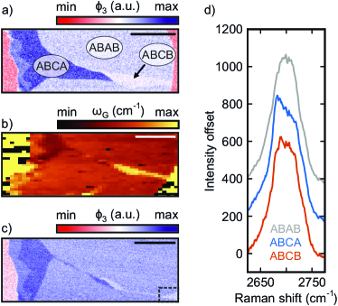
Raman spectra of the G and 2D peak of the three stacking orders are shown in Figures 3 a) and b), respectively (M peaks in the inset). Within individual samples, the G peak position and width show small changes between different domains, even though their absolute values depend on strain and doping 35, 36 and vary between samples. We observe the G-peak position of ABCA stacking to be red-shifted compared to ABAB, which is consistent with the shift observed in ABC and ABA stacked trilayer graphene 14. For ABCB domains, we find the G peak to be at slightly higher energies compared to both other stackings. Notably, the full width at half maximum (FWHM) linewidth of the G peak is the smallest in the ABCA domains and largest in the ABAB domains.
The 2D and M peaks both originate from two-phonon processes and are thus sensitive to the electronic structure as well 37, 38, 39. As a result, both peaks show distinct line shapes for all three stacking orders. Compared to the ABAB 2D peak, which is quite symmetric and featureless, the ABCA 2D peak shows a stronger asymmetry, a sharp feature around 2680 cm-1 and a shoulder around 2640 cm-1. These signatures are consistent with previously reported Raman spectra 14, 40, 41, 39. The ABCB 2D peak appears like an interpolation of the two other peaks: it is more asymmetric than the ABAB peak, but shows a less pronounced feature on the low-energy side compared to the ABCA peak and no low-energy shoulder. The M-peaks 38 show a unique peak shape and position for each stacking, possibly making them the most reliable feature for domain identification despite their low intensity. The Raman spectra confirm the domain assignment by our s-SNOM measurements. A detailed study of the Raman G-, 2D and and M-peaks of ABCB is beyond the scope of this paper.
1.3 Optical conductivity
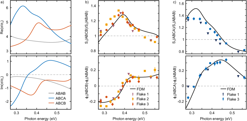
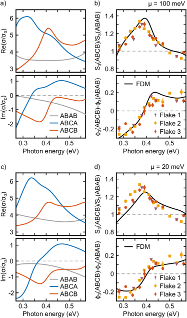
To characterize the different optical conductivities following from the electronic structures, sequential nano-spectroscopy between 0.28 eV and 0.56 eV in conjunction with theoretical modelling was conducted. Figure 4 a) shows the calculated optical conductivities of the three crystallographic stackings ABAB, ABCA and ABCB. The optical conductivities are obtained from tight binding calculations including nearest-neighbor interlayer- and nearest-neighbor intralayer hopping with hopping energies of eV and eV, respectively (see SI S4). This Hamiltonian is optimized to reproduce the band structure at the energies of the s-SNOM measurements 12, 18. The chemical potential ( meV) and a phenomenological broadening ( meV) are chosen to achieve a good match with the s-SNOM data of Flake 3 (see SI S3).
Real- and imaginary part of the conductivity of ABAB are featureless and almost flat between 0.28 and 0.56 eV. Accordingly, we expect a homogeneous amplitude () and phase () response for ABAB when compared to ABCA and ABCB, because these reproduce the characteristic features of real and imaginary part of the conductivity 33.
In total, three different 4LG flakes showing three different domains at 0.34 eV were investigated (Flake 1 in Figure 2; Flake 2 and Flake 3 in SI S1) by s-SNOM. The amplitude and phase contrasts are evaluated line-wise, because of a phase drift, and referenced to the adjacent ABAB values. This referencing overcomes the strong tip dependence of the s-SNOM response of these thin films and makes the results from the three flakes quantitatively comparable.
Amplitude and phase spectra of ABCB- and ABCA-domains, referenced to the ABAB-domains, are shown in Figures 4 b) and c). Note, that Flake 1, 2 and 3 refer to three independently investigated 4LG flakes (see SI S1). The theoretical spectra were obtained from the optical conductivities using a multilayer extension of the finite-dipole model (FDM) 42, in which the graphene layers are taken into account as infinitesimal thin interfaces with a conductivity obtained from tight binding calculations (for Details see SI S2). Both amplitude and phase data reproduce the energy-dependence of the calculated s-SNOM contrast well, constituting the main assignment of the domains in Figure 2 c).
The normalized amplitude data sets S3(ABCB)/S3(ABAB) exhibit a peak at 0.38 eV (Figure 4 b)). The corresponding phase contrast (ABCB)-(ABAB) increases with photon energy and has a zero crossing around eV. For comparison, amplitude and phase contrast data of domain ABCA are plotted in Figure 4 c). Similar domains were investigated on two of the three flakes. The ABCA spectral amplitude and phase data are clearly distinct from the response of ABCB: at low energies down to 0.28 eV the amplitude contrast is much larger than in b) while above, it is monotonically decreasing with photon energy to values below one above eV. The experimental data for both stackings, referenced to ABAB, quantitatively match the calculation at almost all measured photon energies. This shows that the optical response in the entire IR region from 0.28 eV to 0.56 eV can be used to distinguish the three stacking orders. Thus, the detection of ABCB domains in s-SNOM is not restricted to our set-up employing a tunable laser source, but could also be achieved with a more commonly available Helium-Neon laser, which can be operated at 0.366 eV, and has been used to distinguish between TLG and FLG stackings in s-SNOM 31.
1.4 Abundance and stability of ABCB domains
Theoretical calculations suggest that ABCB domains are metastable at a higher total energy than ABAB and ABCA 12, whereas in published experimental work, the stacking had so far not been observed. In total, we have scanned an area of 40000 µm2 of exfoliated tetralayer graphene and found ABCB domains to make up approximately 2% of the total area (ABAB to ABCA were around 71% and 27%, respectively). The largest domain was approximately µm2 in size, whereas most domains are significantly smaller. This might explain why, so far, these domains have been overlooked in published work. Based on the s-SNOM and Raman results described in our current work, in the meantime we were also able to unambiguously verify the existence of ABCB by performing Fourier transform infrared micro-spectroscopy (FTIR) on flakes with largest domains, yielding distinct IR reflectance spectra for the three possible stackings of 4LG (See SI Section S5 and Figure S4). So far, it is not known if the size and abundance of ABCB domains after exfoliation depends on the bulk crystal, but we observe that it varies between exfoliations. This might be due to the applied lateral strain 43, 44 and needs to be investigated more closely.
The ABCB domains were stable over the course of several weeks at ambient conditions as well as when subjected to s-SNOM and Raman measurements at moderate laser powers. At higher laser power, we observed the shrinkage of some domains (for details see SI S1) which has also been observed for metastable rhombohedral TLG 13.
2 Discussion
Our experimental results reveal the existence of ABCB stacked tetralayer graphene domains. This observation is enabled by addressing the low-energy electronic structure through the optical conductivity with a tunable laser between 0.28 and 0.56 eV in an s-SNOM setup. The optical conductivity has unique fingerprints arising from characteristic interband transitions for each stacking which manifest themselves in peaks in the normalized scattering amplitude and phase spectra. These features show a broadening of approximately meV, which is below reported values of 50 meV in comparable FTIR studies 17. By referencing the adjacent domains to each other, we achieved excellent agreement between theory and experiment, establishing s-SNOM as a semi-quantitative tool for nanoscale spectroscopy over a wide energy range in the near-infrared spectral region.
From the stability and abundance of our measured samples, we conclude that ABCB domains are metastable at room temperature, although, the least abundant occurring domains after tape exfoliation. This agrees with theoretical predictions where the energy barrier between ABCB and ABAB is expected to be lower when compared to ABCA and ABCB 12.
The new stacking is of high interest, because it is the thinnest naturally occurring FLG stacking with an intrinsic bandgap 15, 12, 16 and its low energy physics is dominated by valley flat bands which might promote electron-electron interactions favoring correlated states, such as magnetism and unconventional superconductivity. The intricate nature of these states is an interesting avenue for further theoretical 45 and experimental studies. Furthermore, playing to the unique intrinsic narrow band-gap insulating behavior of ABCB graphene, one faces the natural question whether correlated or excitonic physics might play a prominent role. Studying these questions is an intriguing avenue of future research, for which our characterisation of the optical response of ABCB graphene will serve as a convenient starting point.
3 Methods
Exfoliation
We obtain tetralayer graphene flakes by exfoliation of commercially available graphite crystals (Graphenium Flakes, NGS Naturgraphit GmbH). Mechanical cleaving is performed using a dicing tape (1008R, Ultron Systems), which is then pressed onto silicon wafers with an oxide thickness of nm. All processes are performed at room temperature under ambient conditions. No additionally cleaning steps were performed. Suitable flakes were identified via their optical contrast using a standard optical microscope.
s-SNOM
We use a commercially available s-SNOM (NeaSNOM, neaspec GmbH) at photon energies between 0.28 to 0.56 eV for sequential nano-spectroscopy on 4LG in combination with a LN2 cooled InSb detector (Infrared Associates). The s-SNOM is operated in pseudo-heterodyne detection mode, to record amplitude and phase simultaneously. The laser source is a commercially available tunable OPO/OPA laser system (Alpha Module, Stuttgart Instruments) with an energy resolution of meV, which can address the energy range from 0.27 to 0.9 eV. The laser source emits pulses with a pulse length of 1 ps and has a repetition rate of 42 MHz. The s-SNOM is operated at tapping frequencies of 220-270 kHz at tapping amplitudes of 50-60 nm. We extracted the signal from the third demodulation order amplitude and phase. For single imaging with s-SNOM in pseudo-heterodyne detection mode, this pulse width is sufficient in the investigated energy range as recently shown 33, 46.
Raman spectroscopy
Raman maps were taken using a 532 nm laser focused down to a spotsize of approximately 500 nm. The Raman spectra shown in Figure 4, were obtained by averaging the Raman maps within the individual stacking domains. The excitation power was mostly kept to 1.5 mW or below, as higher laser powers occasionally resulted in shrinkage of ABCA and ABCB domains.
This work was supported by the Excellence Initiative of the German federal and state governments, the Ministry of Innovation of North Rhine-Westphalia and the Deutsche Forschungsgemeinschaft. KGW, DS and TT acknowledge support from the Deutsche Forschungsgemeinschaft (DFG) within the collaborative research center SFB 917 and within Grant Agreement No. TA 848/7-1. AR, BB, CS, and LW acknowledge support from the European Union’s Horizon 2020 research and innovation programme under grant agreement No. 881603 (Graphene Flagship), the Deutsche Forschungsgemeinschaft (DFG, German Research Foundation) under Germany’s Excellence Strategy - Cluster of Excellence Matter and Light for Quantum Computing (ML4Q) EXC 2004/1 - 390534769, through DFG (BE 2441/9-1), and the FLAG-ERA grant TATTOOS, by the Deutsche Forschungsgemeinschaft (DFG, German Research Foundation) - 437214324. JBH, LK, AF and DMK acknowledge funding by the Deutsche Forschungsgemeinschaft (DFG, German Research Foundation) under RTG 1995, within the Priority Program SPP 2244 “2DMP” and under Germany’s Excellence Strategy - Cluster of Excellence Matter and Light for Quantum Computing (ML4Q) EXC 2004/1 - 390534769. DMK acknowledges support by the Max Planck-New York City Center for Nonequilibrium Quantum Phenomena. We acknowledge computational resources provided by the Max Planck Computing and Data Facility and RWTH Aachen University under project number rwth0742 and rwth0716.
4 Author Contributions
KGW, JBH, LW, DMK, BB, CS and TT conceived the project. AR and HK fabricated the samples. KGW and DS performed the s-SNOM experiments and theoretical contrast calculations. LC conducted the FTIR measurements. AR, HK and LW carried out the Raman measurements. LW and KGW analysed the experimental data. JBH, LK and AF carried out the theoretical calculation. All authors contributed to writing the manuscript.
5 Competing interests
The authors declare no competing interests.
References
- Zhang et al. 2005 Zhang, Y.; Tan, Y.-W.; Stormer, H. L.; Kim, P. Experimental observation of the quantum Hall effect and Berry’s phase in graphene. Nature 2005, 438, 201–204
- Novoselov et al. 2006 Novoselov, K. S.; McCann, E.; Morozov, S. V.; Fal’ko, V. I.; Katsnelson, M. I.; Zeitler, U.; Jiang, D.; Schedin, F.; Geim, A. K. Unconventional quantum Hall effect and Berry’s phase of 2 in bilayer graphene. Nat. Phys. 2006, 2, 177–180
- Zhou et al. 2021 Zhou, H.; Saito, Y.; Cohen, L.; Huynh, W.; Patterson, C. L.; Yang, F.; Taniguchi, T.; Watanabe, K.; Young, A. F. Isospin magnetism and spin-triplet superconductivity in Bernal bilayer graphene. arXiv:2110.11317 [cond-mat] 2021,
- Zhou et al. 2021 Zhou, H.; Xie, T.; Taniguchi, T.; Watanabe, K.; Young, A. F. Superconductivity in rhombohedral trilayer graphene. Nature 2021, 598, 434–438
- Zhou et al. 2021 Zhou, H.; Xie, T.; Ghazaryan, A.; Holder, T.; Ehrets, J. R.; Spanton, E. M.; Taniguchi, T.; Watanabe, K.; Berg, E.; Serbyn, M.; Young, A. F. Half- and quarter-metals in rhombohedral trilayer graphene. Nature 2021, 598, 429–433
- Kerelsky et al. 2021 Kerelsky, A.; Rubio-Verdú, C.; Xian, L.; Kennes, D. M.; Halbertal, D.; Finney, N.; Song, L.; Turkel, S.; Wang, L.; Watanabe, K.; Taniguchi, T.; Hone, J.; Dean, C.; Basov, D. N.; Rubio, A.; Pasupathy, A. N. Moiréless correlations in ABCA graphene. Proceedings of the National Academy of Sciences 2021, 118, e2017366118
- Balents et al. 2020 Balents, L.; Dean, C. R.; Efetov, D. K.; Young, A. F. Superconductivity and strong correlations in moiré flat bands. Nature Physics 2020, 16, 725–733
- Kennes et al. 2021 Kennes, D. M.; Claassen, M.; Xian, L.; Georges, A.; Millis, A. J.; Hone, J.; Dean, C. R.; Basov, D. N.; Pasupathy, A. N.; Rubio, A. Moiré heterostructures as a condensed-matter quantum simulator. Nature Physics 2021, 17, 155–163
- Cao et al. 2018 Cao, Y.; Fatemi, V.; Fang, S.; Watanabe, K.; Taniguchi, T.; Kaxiras, E.; Jarillo-Herrero, P. Unconventional superconductivity in magic-angle graphene superlattices. Nature 2018, 556, 43–50
- Liu et al. 2020 Liu, X.; Hao, Z.; Khalaf, E.; Lee, J. Y.; Ronen, Y.; Yoo, H.; Haei Najafabadi, D.; Watanabe, K.; Taniguchi, T.; Vishwanath, A.; Kim, P. Tunable spin-polarized correlated states in twisted double bilayer graphene. Nature 2020, 583, 221–225
- Shen et al. 2020 Shen, C.; Chu, Y.; Wu, Q.; Li, N.; Wang, S.; Zhao, Y.; Tang, J.; Liu, J.; Tian, J.; Watanabe, K.; Taniguchi, T.; Yang, R.; Meng, Z. Y.; Shi, D.; Yazyev, O. V.; Zhang, G. Correlated states in twisted double bilayer graphene. Nature Physics 2020, 16, 520–525
- Aoki and Amawashi 2007 Aoki, M.; Amawashi, H. Dependence of band structures on stacking and field in layered graphene. Solid State Communications 2007, 142, 123–127
- Zhang et al. 2020 Zhang, J.; Han, J.; Peng, G.; Yang, X.; Yuan, X.; Li, Y.; Chen, J.; Xu, W.; Liu, K.; Zhu, Z.; Cao, W.; Han, Z.; Dai, J.; Zhu, M.; Qin, S.; Novoselov, K. S. Light-induced irreversible structural phase transition in trilayer graphene. Light: Science & Applications 2020, 9, 174
- Lui et al. 2011 Lui, C. H.; Li, Z.; Chen, Z.; Klimov, P. V.; Brus, L. E.; Heinz, T. F. Imaging Stacking Order in Few-Layer Graphene. Nano Letters 2011, 11, 164–169
- Latil and Henrard 2006 Latil, S.; Henrard, L. Charge Carriers in Few-Layer Graphene Films. Physical Review Letters 2006, 97, 036803
- Min and MacDonald 2008 Min, H.; MacDonald, A. H. Electronic Structure of Multilayer Graphene. Progress of Theoretical Physics Supplement 2008, 176, 227–252
- Mak et al. 2010 Mak, K. F.; Sfeir, M. Y.; Misewich, J. A.; Heinz, T. F. The evolution of electronic structure in few-layer graphene revealed by optical spectroscopy. Proceedings of the National Academy of Sciences 2010, 107, 14999–15004
- Mak et al. 2010 Mak, K. F.; Shan, J.; Heinz, T. F. Electronic Structure of Few-Layer Graphene: Experimental Demonstration of Strong Dependence on Stacking Sequence. Physical Review Letters 2010, 104, 176404
- Lui et al. 2011 Lui, C. H.; Li, Z.; Mak, K. F.; Cappelluti, E.; Heinz, T. F. Observation of an electrically tunable band gap in trilayer graphene. Nature Physics 2011, 7, 944–947
- Berciaud et al. 2014 Berciaud, S.; Potemski, M.; Faugeras, C. Probing Electronic Excitations in Mono- to Pentalayer Graphene by Micro Magneto-Raman Spectroscopy. Nano Letters 2014, 14, 4548–4553, Publisher: American Chemical Society
- Henni et al. 2016 Henni, Y.; Ojeda Collado, H. P.; Nogajewski, K.; Molas, M. R.; Usaj, G.; Balseiro, C. A.; Orlita, M.; Potemski, M.; Faugeras, C. Rhombohedral Multilayer Graphene: A Magneto-Raman Scattering Study. Nano Letters 2016, 16, 3710–3716
- Taubner et al. 2003 Taubner, T.; Hillenbrand, R.; Keilmann, F. Performance of visible and mid-infrared scattering-type near-field optical microscopes. Journal of Microscopy 2003, 210, 311–314
- Fei et al. 2012 Fei, Z.; Rodin, A. S.; Andreev, G. O.; Bao, W.; McLeod, A. S.; Wagner, M.; Zhang, L. M.; Zhao, Z.; Thiemens, M.; Dominguez, G.; Fogler, M. M.; Neto, A. H. C.; Lau, C. N.; Keilmann, F.; Basov, D. N. Gate-tuning of graphene plasmons revealed by infrared nano-imaging. Nature 2012, 487, 82–85
- Chen et al. 2012 Chen, J.; Badioli, M.; Alonso-González, P.; Thongrattanasiri, S.; Huth, F.; Osmond, J.; Spasenović, M.; Centeno, A.; Pesquera, A.; Godignon, P.; Zurutuza Elorza, A.; Camara, N.; de Abajo, F. J. G.; Hillenbrand, R.; Koppens, F. H. L. Optical nano-imaging of gate-tunable graphene plasmons. Nature 2012, 487, 77–81
- Fei et al. 2013 Fei, Z.; Rodin, A. S.; Gannett, W.; Dai, S.; Regan, W.; Wagner, M.; Liu, M. K.; McLeod, A. S.; Dominguez, G.; Thiemens, M.; Castro Neto, A. H.; Keilmann, F.; Zettl, A.; Hillenbrand, R.; Fogler, M. M.; Basov, D. N. Electronic and plasmonic phenomena at graphene grain boundaries. Nature Nanotechnology 2013, 8, 821–825
- Jiang et al. 2016 Jiang, L.; Shi, Z.; Zeng, B.; Wang, S.; Kang, J.-H.; Joshi, T.; Jin, C.; Ju, L.; Kim, J.; Lyu, T.; Shen, Y.-R.; Crommie, M.; Gao, H.-J.; Wang, F. Soliton-dependent plasmon reflection at bilayer graphene domain walls. Nature Materials 2016, 15, 840–844
- Jiang et al. 2017 Jiang, B.-Y.; Ni, G.-X.; Addison, Z.; Shi, J. K.; Liu, X.; Zhao, S. Y. F.; Kim, P.; Mele, E. J.; Basov, D. N.; Fogler, M. M. Plasmon Reflections by Topological Electronic Boundaries in Bilayer Graphene. Nano Letters 2017, 17, 7080–7085
- Jiang et al. 2018 Jiang, L.; Wang, S.; Shi, Z.; Jin, C.; Utama, M. I. B.; Zhao, S.; Shen, Y.-R.; Gao, H.-J.; Zhang, G.; Wang, F. Manipulation of domain-wall solitons in bi- and trilayer graphene. Nature Nanotechnology 2018, 13, 204–208
- Sunku et al. 2018 Sunku, S. S.; Ni, G. X.; Jiang, B. Y.; Yoo, H.; Sternbach, A.; McLeod, A. S.; Stauber, T.; Xiong, L.; Taniguchi, T.; Watanabe, K.; Kim, P.; Fogler, M. M.; Basov, D. N. Photonic crystals for nano-light in moiré graphene superlattices. Science 2018, 362, 1153–1156
- Halbertal et al. 2021 Halbertal, D.; Finney, N. R.; Sunku, S. S.; Kerelsky, A.; Rubio-Verdú, C.; Shabani, S.; Xian, L.; Carr, S.; Chen, S.; Zhang, C.; et al., Moiré metrology of energy landscapes in van der Waals heterostructures. Nature Communications 2021, 12, 242
- Kim et al. 2015 Kim, D.-S.; Kwon, H.; Nikitin, A. Y.; Ahn, S.; Martín-Moreno, L.; García-Vidal, F. J.; Ryu, S.; Min, H.; Kim, Z. H. Stacking Structures of Few-Layer Graphene Revealed by Phase-Sensitive Infrared Nanoscopy. ACS Nano 2015, 9, 6765–6773
- Jeong et al. 2017 Jeong, G.; Choi, B.; Kim, D.-S.; Ahn, S.; Park, B.; Kang, J. H.; Min, H.; Hong, B. H.; Kim, Z. H. Mapping of Bernal and non-Bernal stacking domains in bilayer graphene using infrared nanoscopy. Nanoscale 2017, 9, 4191–4195
- Wirth et al. 2021 Wirth, K. G.; Linnenbank, H.; Steinle, T.; Banszerus, L.; Icking, E.; Stampfer, C.; Giessen, H.; Taubner, T. Tunable s-SNOM for Nanoscale Infrared Optical Measurement of Electronic Properties of Bilayer Graphene. ACS Photonics 2021, 8, 418–423
- Keilmann and Hillenbrand 2004 Keilmann, F.; Hillenbrand, R. Near-field microscopy by elastic light scattering from a tip. Philosophical Transactions of the Royal Society of London. Series A: Mathematical, Physical and Engineering Sciences 2004, 362, 787–805
- Toporski et al. 2018 Toporski, J., Dieing, T., Hollricher, O., Eds. Confocal Raman Microscopy; Springer Series in Surface Sciences; Springer International Publishing: Cham, 2018; Vol. 66
- Neumann et al. 2015 Neumann, C.; Reichardt, S.; Venezuela, P.; Drögeler, M.; Banszerus, L.; Schmitz, M.; Watanabe, K.; Taniguchi, T.; Mauri, F.; Beschoten, B.; Rotkin, S. V.; Stampfer, C. Raman spectroscopy as probe of nanometre-scale strain variations in graphene. Nat. Commun. 2015, 6, 8429
- Malard et al. 2009 Malard, L.; Pimenta, M.; Dresselhaus, G.; Dresselhaus, M. Raman spectroscopy in graphene. Physics Reports 2009, 473, 51–87
- Cong et al. 2011 Cong, C.; Yu, T.; Saito, R.; Dresselhaus, G. F.; Dresselhaus, M. S. Second-order overtone and combination raman modes of graphene layers in the range of 1690-2150 cm-1. ACS Nano 2011, 5, 1600–1605
- Torche et al. 2017 Torche, A.; Mauri, F.; Charlier, J.-C.; Calandra, M. First-principles determination of the Raman fingerprint of rhombohedral graphite. Physical Review Materials 2017, 1, 041001
- Nguyen et al. 2014 Nguyen, T. A.; Lee, J.-U.; Yoon, D.; Cheong, H. Excitation energy dependent Raman signatures of ABA- and ABC-stacked few-layer graphene. Scientific Reports 2014, 4, 4630
- Geisenhof et al. 2019 Geisenhof, F. R.; Winterer, F.; Wakolbinger, S.; Gokus, T. D.; Durmaz, Y. C.; Priesack, D.; Lenz, J.; Keilmann, F.; Watanabe, K.; Taniguchi, T.; Guerrero-Avilés, R.; Pelc, M.; Ayuela, A.; Weitz, R. T. Anisotropic Strain-Induced Soliton Movement Changes Stacking Order and Band Structure of Graphene Multilayers: Implications for Charge Transport. ACS Applied Nano Materials 2019, 2, 6067–6075
- Hauer et al. 2012 Hauer, B.; Engelhardt, A. P.; Taubner, T. Quasi-analytical model for scattering infrared near-field microscopy on layered systems. Optics Express 2012, 20, 13173–13188
- Yang et al. 2019 Yang, Y.; Zou, Y. C.; Woods, C. R.; Shi, Y.; Yin, J.; Xu, S.; Ozdemir, S.; Taniguchi, T.; Watanabe, K.; Geim, A. K.; Novoselov, K. S.; Haigh, S. J.; Mishchenko, A. Stacking Order in Graphite Films Controlled by van der Waals Technology. Nano Letters 2019, 19, 8526–8532
- Nery et al. 2020 Nery, J. P.; Calandra, M.; Mauri, F. Long-Range Rhombohedral-Stacked Graphene through Shear. Nano Letters 2020, 20, 5017–5023
- Klebl et al. 2022 Klebl, L.; Fischer, A.; Hauck, J. B.; Wirth, K. G.; Rothstein, A.; Beschoten, B.; Stampfer, C.; Waldecker, L.; Taubner, T.; Kennes, D. Investigation of possible correlated phases in quadlayer graphene. In preparation 2022,
- Lu et al. 2021 Lu, J.; Wirth, K. G.; Gao, W.; Heßler, A.; Sain, B.; Taubner, T.; Zentgraf, T. Observing 0D subwavelength-localized modes at ~100 THz protected by weak topology. Science Advances 2021, 7, eabl3903
- Cvitkovic et al. 2007 Cvitkovic, A.; Ocelic, N.; Hillenbrand, R. Analytical model for quantitative prediction of material contrasts in scattering-type near-field optical microscopy. Optics Express 2007, 15, 8550
- Zhan et al. 2013 Zhan, T.; Shi, X.; Dai, Y.; Liu, X.; Zi, J. Transfer matrix method for optics in graphene layers. Journal of Physics: Condensed Matter 2013, 25, 215301
- Kubo 1957 Kubo, R. Statistical-Mechanical Theory of Irreversible Processes. I. General Theory and Simple Applications to Magnetic and Conduction Problems. Journal of the Physical Society of Japan 1957, 12, 570–586, _eprint: https://doi.org/10.1143/JPSJ.12.570
- Grüneis et al. 2008 Grüneis, A.; Attaccalite, C.; Wirtz, L.; Shiozawa, H.; Saito, R.; Pichler, T.; Rubio, A. Tight-binding description of the quasiparticle dispersion of graphite and few-layer graphene. Phys. Rev. B 2008, 78, 205425
Supplementary material: Experimental observation of ABCB stacked tetralayer graphene
S1 Stability and abundance
In Figure S1 the optical phase () and a Raman map of the 4LG flake labeled Flake 2 in the main text are shown over the course of several measurements. The phase image () in Figure S1 a) is recorded at a photon energy of 0.34 eV. The 4LG flake can be clearly distinguished from the SiO2 substrate on the left (red area). Three regions on the 4LG are marked with their respective stacking. The domain with the weakest contrast towards the SiO2 is ABCB and the strongest ABCA.
The Raman map around the 2D peak recorded after the s-SNOM measurements is depicted in Figure S1 b). The ABCA-domain shrunk in the middle of the image, while the ABCB-domain is still present. However, due to the limited resolution of the Raman setup, the exact shape of the domains is difficult to determine. Subsequent s-SNOM measurements repeated at 0.34 eV are depicted in Figure S1 c). The ABCA-domain has a similar size to what can be expected from the Raman in Figure S1 b), while the ABCB-domain shrunk again to a small stripe and a triangluar feature at the right side of the image. This feature is indicated by a black dashed rectangle, which corresponds to the region investigated with IR nano-spectroscopy. In Figure S1 d) Raman spectra around the 2D peak corresponding to the map in Figure S1 b) are shown. The different domains exhibit similar features like in Figure 3 b).
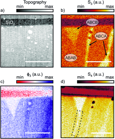
In Figure S2 a) the topography of the 4LG flake labeled as Flake 3 in the main text is shown. The topography image of the 4LG is featureless, only a few dirt particles and the SiO2 substrate can be identified, indicating a homogenous number of four graphene layers.
In the corresponding optical amplitude (S3) and phase image () in Figure S2 b) and c) recorded at a photon energy of 0.34 eV the flake can be clearly distinguished from the SiO2 substrate. It shows three different amplitude and phase signals on the topographically featureless 4LG. The corresponding domains are indicated by ABAB, ABCA and ABCB. ABAB-domains cover the largest part of the 4LG . Two small domains of the largest contrast correspond to ABCA stacking. The triangular shaped ABCB-domain is located at the edge between 4LG and the SiO2 and has an amplitude signal between those of ABAB- and ABCA-domain. In the phase image in Figure S2 c) the same three domains can be identified. Again, the phase response is the largest with respect to the SiO2 for the ABCA-domain and weakest for ABCB.
During our investigations, the domains of Flake 1 (main text) remained stable over several s-SNOM and Raman measurements (over the course of several weeks). For Flake 2 shown in Figure S1, however, we observed the consecutive collapse of a large ABCB domain to a small triangular shaped domains after Raman mapping at laser powers in the range of 3 mW. Such a change in the stacking order has been reported for TLG 13, albeit for significantly higher laser power. The third investigated flake (Flake 3, Figure S2) also shows a triangular shaped similar sized domain of ABCB stacking, possibly a remnant of a collapsed larger domain. This argument is supported by investigations of the respective area with s-SNOM at a wavelength of 10.6 µm (Figure S2 d)), which reveals a small boundary like feature, indicated by the black box, similar to a shear soliton observed in bilayer graphene 26 and TLG 28. The energy barrier between ABCB and ABAB stacking is expected to be much lower compared to the transition from ABCA to ABAB 12. This instability might hamper device fabrication, because the ABCB stacking can transform to energetically favorable Bernal stacking, similar to metastable rhombohedral graphene upon stress or strain during device fabrication 41.
5.1 S2 s-SNOM contrast calculation
The s-SNOM contrast for the 4LG/SiO2/Si layer stack is calculated with the finite dipole model 47 with an extension for layered samples 42 as described in 33.
The effective polarizability of the tip-sample system is calculated via
| (S1) |
where is the tip radius, is the effective length of the assumed sphere and . The detailed description of the model can be found in 42, 47.
| (S2) |
where is the tip height above the sample and g corresponds to a fraction of the total induced charge. The n-th Fourier component needs to be included to account for the higher harmonic demodulation of . The final amplitude and phase contrast depend solely on the third order Fourier component of because the far-field coefficients can be neglected here.
| (S3) |
| (S4) |
Parameters of the FDM are summarized in Table 1. We replace the electrostatic reflection coefficient with a Fresnel reflection coefficient 42 for a single dominant in-plane wave vector cm-1, comparable to the inverse of the expected tip radius of cm-1. To calculate the Fresnel coefficients for the stack, we use the transfer matrix method (TMM) for graphene layers with p-polarized light 48. In our model the tetralayer graphene is infinitesimal thin and a plane interface.
S3 s-SNOM contrasts for different chemical potentials
In Figure S3 a) and c) the optical conductivity of the three stackings is plotted, calculated for a broadening of meV and chemical potentials of and meV, respectively. In b) and d) same amplitude and phase data as in Figure 4 are plotted for ABCB referenced to ABAB. The calculated FDM spectra are shown for two different chemical potential. All three amplitude data sets show a higher peak at 0.38 eV, which can be either attributed to a smaller broadening or an increased chemical potential. For a change in the chemical potential, we expect a shift of the characteristic crossing of 1 and 0 in amplitude and phase, respectively. Furthermore, this also influences the contrast strength. A change in would result in more pronounced features such as the peak in amplitude around 0.4 eV. For Flake 1 and Flake 2 the data fit better to 100 meV, especially the crossing of 1 in the amplitude is better reproduced. There are also indications for a smaller broadening, because amplitude data of Flake 1 indicate a sharper left flank and Flake 2 a more pronounced peak.
S4 Calculation of optical conductivity
For the calculation of the dynamic optical conductivity we employ the Kubo formula 49
| (S5) |
where are the eigenenergies of the Hamiltonian in band at momentum point and are the corresponding eigenvectors. The case of has to be considered separately and results in . is the -direction component of the velocity operator defined as which can be expressed in the momentum-site basis as
| (S6) |
with a vector pointing to a site in the lattice and being a lattice vector. We chose the temperature to be room temperature ( eV) and choose the broadening as meV. We chose a simple tight-binding Hamiltonian of the form
| (S7) |
consisting of only nearest-neighbor intralayer (in a distance Å) and nearest-neighbor interlayer hopping (in a distance Å) with hopping energies of eV and eV. We shift the Fermi energy to meV. The modeling parameters, Fermi-energy and broadening were tweaked for the best agreement with the experimental results.
For the calculations of the DOS and the bandstructure in Fig. 1, we employ a Slonzecewski-Weiss-McClure (SWMC) Hamiltonian, with parameters chosen based on Ref. 50 summarized in Table 2. The Hamilton-matrix can be constructed as
| (S8) |
where and are site indices within the unit cell, marks the type of the lattice and is either ABAB, ABCA or ABCB and is one if is an -site and otherwise. and iterate over all unit cells in the infinite lattice, gives the vectorial distance between the unit cells and gives the distance between site and the image of site shifted by and unit-cell vectors. is the real-space distance associated with each of the hopping parameters is listed in the third column of Table 2.
| Name | Value in eV | Distance in Å |
|---|---|---|
| , A site | ||
| , A site | ||
| , A site |
The values for the are chosen such that we roughly reproduce the low energy behavior of the bandstructures from Ref. 12. Therefore, the model is a good representation of the low energy degrees of freedom near half-filling.
S5 FTIR measurements of tetralayer graphene
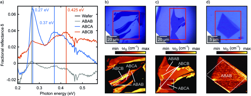
The optical properties of few layer graphene are determined by its optical conductivity, which differs between the different crystal polytypes18. Therefore, the stacking order in few layer graphene can be determined by infrared far-field spectroscopy 18, 17 in the range between 0.2 and 1 eV. The influence of environmental effects, such as doping, on the infrared response of tetralayer graphene is expected to be reduced compared to thinner flakes 18, making far-field spectroscopy a reliable technique. Requirement for the investigation with this method, however, are domains of sufficient size due to the optical diffraction limit. Within a set of approximately 50 flakes scanned by Raman spectroscopy, we identified one suitable ABCB domain. The flake (shown in Fig S4 b) exhibits an ABCB domains of approximately µm2, adjacent to both ABCA and ABAB stacking.
Fourier transform infrared spectroscopy (FTIR) measurements on the three flakes shown in S4 reveal the infrared response of ABAB, ABCA and ABCB stacking orders. All measurements were performed in reflection geometry as the flakes are exfoliated onto SiO2/Si substrates. We calculate the fractional change of the reflectance as following:
| (S9) |
where is the reflectance of the flake and is the reflectance of the substrate. The ABAB stacking is featureless and exhibits only two small peaks at 0.26 eV and above 0.6 eV. The ABCA stacking exhibits two peaks, a pronounced one at 0.27 eV and a weaker one at 0.37 eV. This in good agreement with literature data on ABAB and ABCA stacked 4LG 18. The fractional reflectance of ABCB stacking has a peak at 0.425 eV, which can be distinguished from the higher energy peak of ABCA by a shift towards higher energy and a slightly higher amplitude. The prominent peak of ABCA at lower energies is absent. The peak at 0.425 eV agrees well with the peak position in the real part of the conductivity (c.f. Figure 4a). The same peak as in the ABAB stacking at 0.26 eV is also present, because the surrounding of the ABCB stacking consists mostly of ABAB stacking which also contributes to the signal due to the non perfect aperture and the diffraction limit of infrared radiation. The peaks in the FTIR spectra correspond to the splitting between the conduction bands and are thus unique for each stacking order 18, 17. This is the same principle as for the s-SNOM measurements presented in Figure 4 of the main text, but lacking the sub-diffraction limit spatial resolution of s-SNOM.