Extended Data for
Spin Cross-Correlation Experiments in an Electron Entangler
Arunav Bordoloi
Department of Physics, University of Basel, Klingelbergstrasse 82, CH-4056 Basel, Switzerland
correspondence to: arunav.bordoloi@unibas.ch or andreas.baumgartner@unibas.ch
Valentina Zannier
NEST, Istituto Nanoscienze-CNR and Scuola Normale Superiore, Piazza San Silvestro 12, I-56127 Pisa, Italy
Lucia Sorba
NEST, Istituto Nanoscienze-CNR and Scuola Normale Superiore, Piazza San Silvestro 12, I-56127 Pisa, Italy
Christian Schönenberger
Department of Physics, University of Basel, Klingelbergstrasse 82, CH-4056 Basel, Switzerland
Swiss Nanoscience Institute, University of Basel, Klingelbergstrasse 82, CH-4056 Basel, Switzerland
Andreas Baumgartner
Department of Physics, University of Basel, Klingelbergstrasse 82, CH-4056 Basel, Switzerland
Swiss Nanoscience Institute, University of Basel, Klingelbergstrasse 82, CH-4056 Basel, Switzerland
correspondence to: arunav.bordoloi@unibas.ch or andreas.baumgartner@unibas.ch
Table 1: Spin dependence for competing two electron transport processes in a CPS device. We note that LPT + SET (process 4) may mimick the CPS charge signal, but can be distinguished using spin filtering.
Process
Parallel state ()
Antiparallel state ()
Cooper Pair Splitting (CPS)
Local Pair Tunneling (LPT)
CPS + Single Electron Tunneling (SET)
LPT + SET
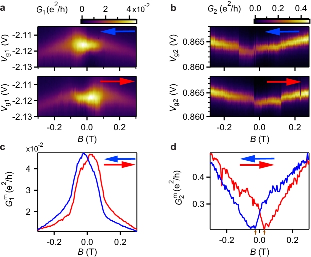
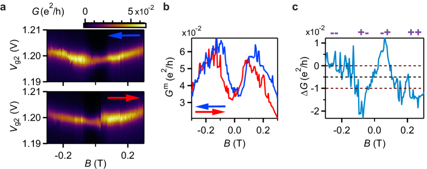
Figure 1: Magnetoconductance (MC) measurements.a,b Down-(blue arrow) and up-sweep (red arrow) maps of and respectively, as a function of the external magnetic field and the gate voltage (a) and (b). c,d Maximum conductance and as a function of extracted from (a) and (b) for the up (red) and down (blue) sweep.
In order to demonstrate the presence of a non-zero stray magnetic field at each QD position, we measure () as a function of () for a particular Coulomb blockade resonance of the respective QD at a series of external magnetic fields applied parallel to the FSG axes. Such maps of and are shown in extended data figures 1a and 1b for increasing (red arrow) and decreasing (blue arrow) magnetic fields. We note that is first swept to large values, i.e. T or T, to ensure the formation of a single domain along the FSG axes. Both, and , show a clear hysteresis with a strong dependence on the sweep direction of , corresponding to a remnant magnetization in both FSGs and a finite on both QDs. To explicitly demonstrate this, we extract the maximum conductance and for QD1 and QD2, as plotted in extended data figures 1c and 1d respectively, for increasing (red) and decreasing (blue) .
In the up sweep, we find that decreases roughly linearly with increasing followed by a relatively sharp decrease around . At mT, achieves it minimum value, and starts to increase with more positive . The down sweep can be described in a similar manner, but mirror symmetric around . Qualitatively, can be understood as a smooth magnetoconductance (MC) of QD2 [1, 2], which changes relatively abruptly when the corresponding FSG reverses its magnetization direction. The red curve shows a relatively abrupt change at mT at which the FSG magnetization is reoriented, as indicated by the brown arrows in extended data figure 1d.
Similar to , exhibits a clear hysteresis around as shown in extended data figure 1c. In the up-sweep (red curve), increases roughly linearly with increasing up to mT, followed by a steep increase with a maximum at mT and a steep decrease around mT. For mT, shows a roughly linear decrease with more positive . The down sweep (blue curve) is mirror-symmetric with respect to the up sweep (red curve) at .
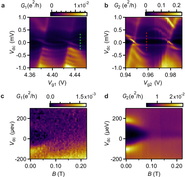
Figure 2: Bias spectroscopy and superconducting gap measurement.a,b Differential conductances and respectively, as a function of the source-drain bias voltage . c,d and as a function of and the external magnetic field for the cross sections marked by the green and red dashed lines in (a) and (b) respectively. Both measurements show a critical magnetic field of mT for the superconducting contact.
In this section, we present bias spectroscopy experiments for the individual QDs to determine their transport properties at zero external magnetic field, , applied in the substrate plane along the FSG long axes. Extended data figures 2a and 2b show colorscale plots of and as a function of the applied bias voltage and the gate voltages and , respectively. We extract an addition energy of meV and meV for QD1 and QD2, and a superconducting gap of eV in both datasets. The cross lever arms (across the the S contact) are one order of magnitude lower compared to the lever arm of a close by FSG, which allows one to independently tune the QDs. In order to characterize the superconductor, we apply an in-plane external magnetic field parallel to the FSG long axes. and as a function of and , along the cross sections marked by the green and red dashed line in extended data figures 2a and 2b, are plotted in extended data figures 2c and 2d, respectively. We find that the superconducting gap is suppressed at a critical magnetic field of mT. Clearly, the magnitudes of and cannot be larger than at the position of the superconductor, and are much smaller than can be resolved here, considering that shows a maximum () at , i.e. no detectable offset field at the position of S.
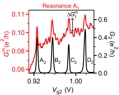
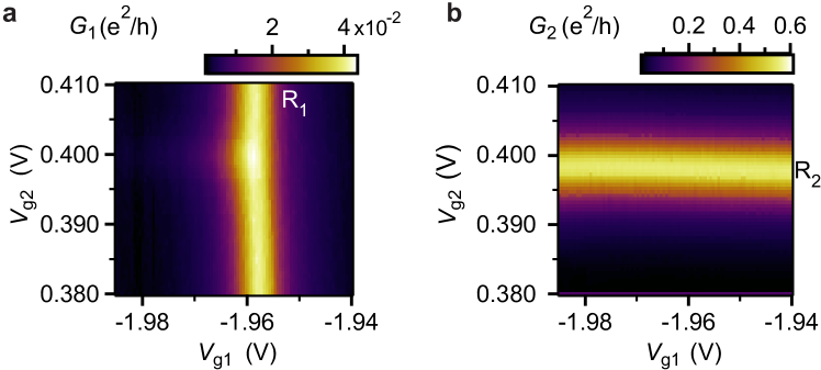
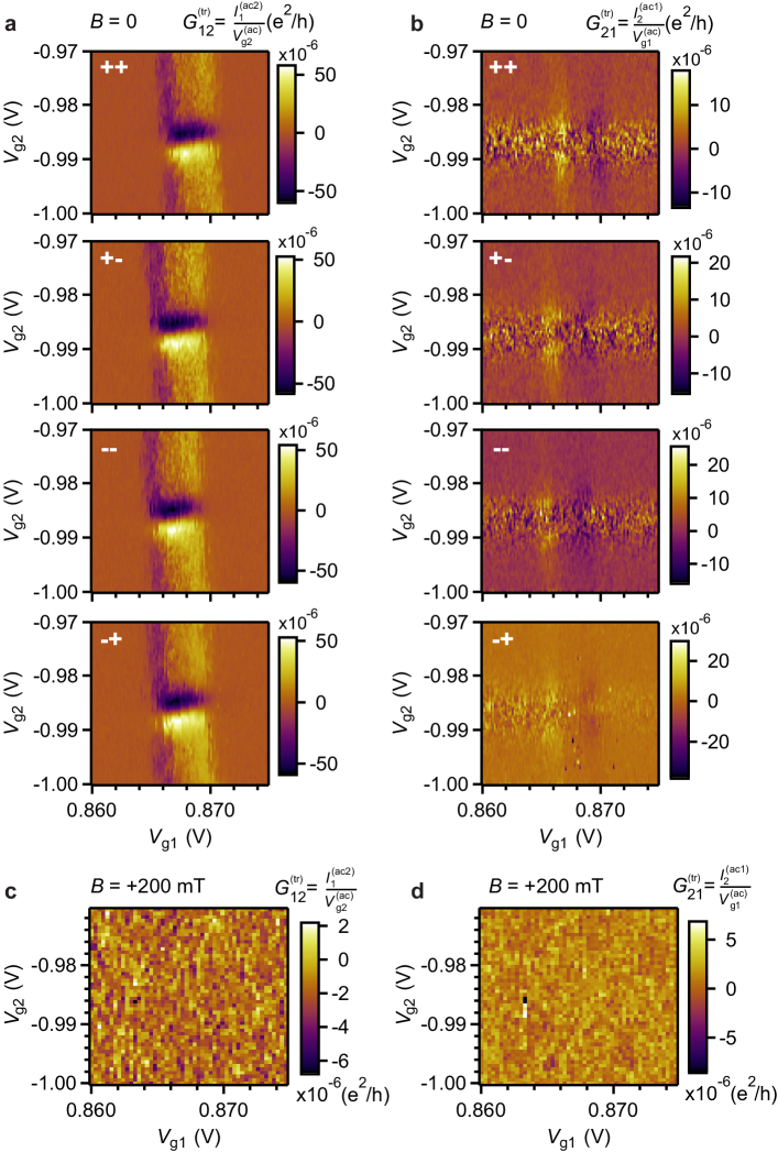
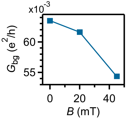
Figure 3: for the QD resonance A1 in figure 1d of the main text . Maximum conductance as a function of gate voltage for resonance of QD1, showing peaks whenever QD2 is tuned across any of the Coulomb blockade resonances A2-D2.Figure 4: Normal-state measurements at mT.a,b Differential conductances and respectively, measured simultaneously as a function of and at a bias voltage of and an external magnetic field of mT. c Maximum conductance as a function of gate voltage at mT (red curve), showing a much smaller modulation and no obvious correlation to , when the latter (black curve) is tuned through Coulomb blockade peaks using . d Maximum conductance as a function of gate voltage at for the same resonances as in c, showing peaks when is tuned across Coulomb blockade resonances by . We note that the scale of is adjusted to show the same conductance span.Figure 5: Data supporting figure 2 of the main text.a,b Differential conductances and respectively, as a function of and at zero bias voltage, and zero external magnetic field, , for the resonance crossing (R1, R2) described in figure 2 in the main text.Figure 6: Transconductance Measurements for the four magnetization states at and mT.a,b,c,d Transconductance (a,c) and (b,d) measured as a function of and with a bias of eV applied to S, for each magnetization state () indicated in each figure, at (a,b) and mT (c,d) for the resonance crossings M1 and N2 in figure 3 of the main text. We do not observe any modulation of the transconductance if S is in the normal-state (mT).Figure 7: Conductance maxima modulation at finite magnetic fields for main text figure 4.a,b Differential conductances and respectively, measured as a function of and at zero bias and . c Maximum conductance as a function of the gate voltage for the resonances in a and b, showing peaks when is tuned across Coulomb blockade resonances by . d,e,f Modulation of the conductance maximum, , for all four magnetization states () measured at (d), mT (e), and mT (f) for the resonance crossing (X1,X2).Figure 8: Background conductance versus the external magnetic field . Here we plot the background conductance at the respective resonance position, extracted from the parabolic fits discussed in the main text. This background is most probably dominated by LPT processes. We note that decreases with increasing , as expected for the local processes (see extended data table 1) and for an increasing QD spin polarization.Figure 9: Estimates for the characteristic switching fields B.a Down-(blue arrow) and up-sweep (red arrow) maps of the differential conductance as a function of and the gate voltage for a two-terminal measurement between the two normal (N) contacts, with the middle superconducting contact (S) floating. b Maximum conductance as a function of extracted from figure a for the up (red) and down (blue) sweep. c as a function of derived from figure b, showing estimates for all parallel and antiparallel magnetization states.
To estimate the characteristic switching fields of the FSGs, we operate the device in a spin-valve configuration, i.e. we perform standard two-terminal lock-in measurements with the two QDs in series and with S kept floating, and measure the differential conductance as a function of and for increasing (red) and decreasing (blue) as shown in extended data figure 9a. The corresponding maximum conductance is plotted in extended data figure 9b. In the up sweep (red curve), first increases with increasing , followed by a maximum at mT and a subsequent decrease with a minimum at mT. Around , starts to increase again with small positive , followed by another maximum at mT, and a further decrease towards more positive . The down sweep (blue curve) is mirror symmetric to the up sweep (red curve) at .
To determine the parallel and antiparallel magnetization states, we plot , i.e. we subtract the blue from the red curve, as a function of in extended data figure 9c, where and refer to the up (red) and down (blue) sweep in extended data figure 9b. We first assign an effective average zero level of the measured data, as indicated by the black dashed line in extended data figure 9c. We then define a lower and upper conductance limit (brown dashed lines) for significant deviation of from the average zero. We use the values at which the upper horizontal brown dashed line meets as the two switching fields, mT and mT, respectively. We obtain similar switching field values for the lower horizontal brown dashed line. Therefore, for magnetic field values between , the FSGs are oriented in an antiparallel magnetization configuration.
References
[1]
G. Fabian et al.Magnetoresistance engineering and singlet/triplet switching in InAs nanowire quantum dots with ferromagnetic sidegates,
Physical Review B, 94, 195415, 2016.
[2]
A. Bordoloi et al.A double quantum dot spin valve,
Communications Physics, 3, 2020.