Memristor-based cryogenic programmable DC sources for scalable in-situ quantum-dot control
Abstract
Current quantum systems that are based on spin qubits are controlled by classical electronics located outside the cryostat at room temperature. This approach creates a major wiring bottleneck, which is one of the main roadblocks toward truly scalable quantum computers. Thus, we propose a scalable memristor-based programmable DC source that can be used to perform biasing of quantum dots inside the cryostat (i.e., in-situ). This novel cryogenic approach would enable us to control the applied voltage on the electrostatic gates by programming the resistance of the memristors, thus storing in the latter the appropriate conditions to form the quantum dots. In this study, we first demonstrate multilevel resistance programming of TiO-based memristors at , which is an essential feature to achieve voltage tunability of the memristor-based DC source. We then report hardware-based simulations of the electrical performance of the proposed DC source. A cryogenic TiO-based memristor model fitted on our experimental data at was used to show a voltage range and in-situ memristor-based DC source. Finally, we simulate the biasing of double quantum dots, enabling sub-2 minutes in-situ charge stability diagrams. This demonstration is a first step towards more advanced cryogenic applications for resistive memories, such as cryogenic control electronics for quantum computers.
I Introduction
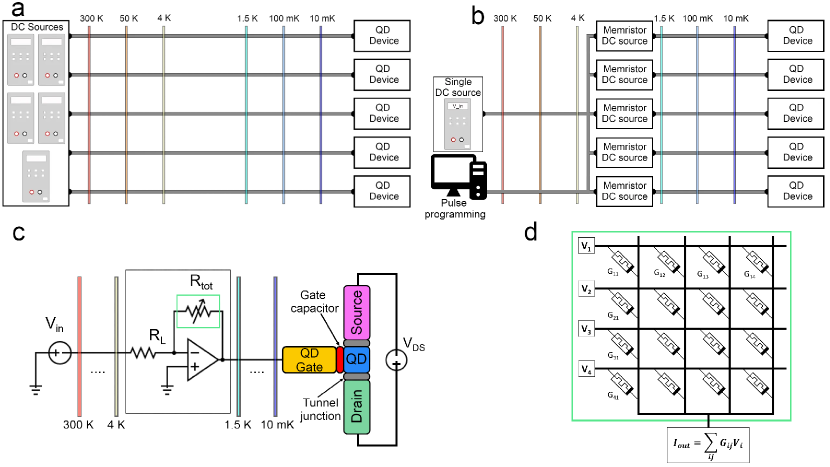
Silicon quantum dots (QDs) are among the leading candidates for large scale integration of qubits given their compatibility with industrial semiconductor fabrication processes Pillarisetty_2018qubits ; zwerver2021qubits , which may enable mass production and easier co-integration with control electronics. Moreover, semiconductor qubits benefit from a small qubit pitch, a long coherence time, and high gate fidelity Veldhorst2014 ; Yoneda2017 ; Watson2018 ; Zajac2017 . However, quantum error correction and millions of physical qubits will be required to enable key industrial applications, such as encryption, quantum machine learning, or drug synthesis. The current approach to realize a quantum dot-based computer requires the qubit chips to be operated at or below Yang2020 ; Petit2020 , while its control charge carriers for state manipulation and readout are placed outside of the dilution refrigerator (see Fig. 1a). In particular, the number of quantum-dot gates that are required to properly confine the charge carriers can range from one to up to six for specific quantum dot designs Geck2019 , and as many dedicated DC sources and cables per qubit. Although the control approach that is depicted in Fig. 1a has enabled important demonstrations over the past 20 years, it will become very cumbersome for few hundred qubits and may even be unachievable for the million of physical qubits that are required for fault tolerant quantum computing Bardin2018 . To avoid this wiring bottleneck, integrated cryogenic control platforms are being developed to control a larger number of spin qubits Vandersypen2017 ; Geck2019 ; Bardin2018 ; ruffino2021integrated ; Xue2021 ; Pauka2021 , while limiting the control electronics required at room temperature (See Fig. 1b).
To identify and reach the correct electronic regime, it is necessary to individually tune all of the quantum-dot gate biases (see Fig. 1a and b) using DC signals, typically in the range with at least a resolution, while maintaining a thermal budget in the order of a milliwatt or below per DC source Vandersypen2017 ; Geck2019 . A first integrated solution based on switched-capacitor circuits and charge-locking, which is conceptually close to dynamic random access memories (DRAMs), has been proposed to perform simultaneous charge carrier confinement for several quantum dotsXuSwitchedCapa2020 ; ruffino2021integrated . However, this approach requires qubits that have similar electrical behaviour, which has yet to be demonstrated for silicon spin qubits. To maintain the desired bias voltage applied to the quantum-dot gate, the switched-capacitor charge needs to be refreshed periodically. Meanwhile, TiO2-based memristors Chua1971 ; Strukov2008 exhibit promising features, such as non-volatility, multilevel resistance state programming Alibart2012 and CMOS-compatible fabrication processes mesoudy2021CMOS . The memristor is used as the core component of the DC source. Its resistance value depends on its internal state. This resistance state has the particularity of being adjustable by external stimuli, such as DC sweeping or voltage pulses LeCun2015 ; Amirsoleimani2020 , which enables the voltage programmability of the DC source. Moreover, the conduction mechanisms and temperature dependent DC behavior of memristors based on transition metal oxides have been studied at cryogenic temperatures down to Beilliard2020 ; Fang2015 ; Blonkowski2015 ; Pickett2011 ; Zhang2014 ; Alagoz2019 ; Voronkovskii2019 , hinting at hybrid CMOS-memristor control circuits for quantum systems. The co-integration of a memristor-based biasing circuit and QDs will benefit from the recently demonstrated operation of spin qubits at Yang2020 ; Petit2020 relaxing the power dissipation restrictions. This approach would make it possible to control the applied voltage on the gates by changing the resistance of the memristors in a non-volatile manner, thus storing in the latter the appropriate conditions for the QDs to be formed. This on-chip co-integration would require a single I/O to bias several quantum dots, thus paving the way for scalable quantum computers on silicon.
In this paper, we propose a memristor-based DC source set to operate at to first control the voltage bias applied to the gates of a silicon quantum dot cooled to . However, the perspective of spin qubits at in the near future would allow a co-integration with the memristor-based DC source enabling scalability as both technologies are CMOS-compatible mesoudy2021CMOS ; Maurand2016 . Using a feedback resistance tuning algorithm, we experimentally demonstrate the multilevel resistance programmability of CMOS-compatible Al2O3/TiO2-x memristor crosspoints mesoudy2021CMOS at . In addition, we conduct extensive hardware-based simulations of a memristor-based programmable gain amplifier (PGA) to optimize the design of the memristor feedback resistor, and show that this approach meets the voltage range and resolution criteria for in-situ biasing of quantum dots.
II Concept
Figure 1a shows a typical experimental setup for solid-state spin qubits that operate at a temperature of or below with optimal operation in the tens of millikelvins. DC biases are generated by rack-sized electronics at room temperature and transported by DC lines to the qubits in the dilution refrigerator. This approach imposes a limit on the number of biasing lines that can be integrated. We propose a programmable gain amplifier (PGA) as a biasing solution where the variable feedback resistor is based on a memristor circuit (See Fig. 1c, d). The resistance of each memristor can be finely tuned individually due to the analog behaviour of resistive memories. Write pulses are used to accurately program the resistance of the memristors. In the context of the PGA, these pulses can be applied using a low-dissipation cryogenic FPGA Artix_cryo_charbon . A single DC source that provides a fixed voltage at room temperature is required to supply multiple PGA circuits placed at the -stage (See Fig. 1b, c) limiting the control electronic that is required at room temperature and thus limiting the number of cables going in the cryostat.
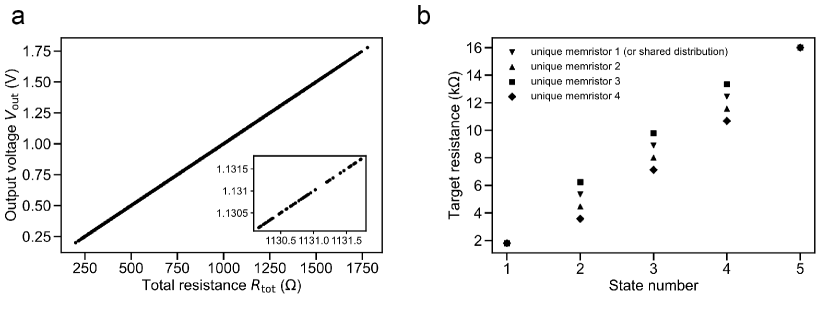
Based on the circuit parameters in Fig. 1c, we can fully determine the theoretical electrical characteristics of the memristor-based DC source. The output voltage of the PGA is determined by the amplification factor , where the load resistor is constant. With a common supply voltage supplied to all of the horizontal lines of the memristor crossbar array, the total resistance of the crossbar is given by , where represent the position of a memristor in the crossbar (see Fig. 1d). By programming distinct resistance states for each memristor, the feedback resistor can take a maximum of distinct resistance values, where is the number of memristor in the crossbar circuit. Finally, we can define the theoretical voltage range and the optimal voltage resolution of the memristor-based DC source:
| (1) |
| (2) |
where and are the resistance of the memristor in the lowest resistance state and the highest resistance state, respectively.
III Thermal budget and power dissipation
The power dissipated by the circuit in the dilution fridge is an important consideration when designing cryogenic control electronics for quantum systems. For the memristor-based DC source, the two sources of dissipation are the operational amplifier and the memristors in the feedback loop placed at (see Fig. 1c). On the one hand, the most recent custom cryogenic operational amplifier from Ref. cryo_ampli_le_guevel_2020 dissipates , while commercial amplifiers characterized at are expected to dissipate Proctor2015 . On the other hand, the power dissipated by the memristors is introduced by the Joule heating proportional to the current flowing in the feedback loop. This dissipation is maximized when the memristor-based DC source delivers the maximum output voltage:
| (3) |
where the maximum feedback loop resistance. Our current memristors feature a -HRS, leading to a power dissipation of for a supply voltage required to achieve a supply range. Hence, the total power dissipation of a single memristor-based DC source is in the order of a milliwatt. If we assume that this power is entirely dissipated on-chip, then an approximately 800 memristor-based DC source could be placed at the stage assuming cooling power. This number is currently bottlenecked by the low HRS reachable with our memristor devices. Increasing the HRS would allow us to reduce the input voltage , and thus the power dissipated, while keeping a -range.
IV Experimental results
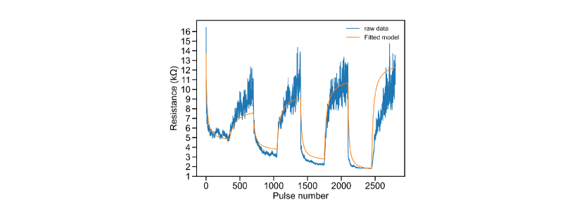
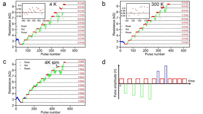
Demonstrating reversible, non-volatile, and linear resistance programming of resistive memory devices at cryogenic temperatures would offer opportunities for hybrid memristor–CMOS cryogenic electronics. To accurately tune resistance states, we use a simple feedback algorithm from Ref. Alibart2012 . At each step, we apply a write pulse of negative amplitude to increase the resistance of the device or a positive amplitude to decrease its resistance, followed by a / read pulse to evaluate the current resistance state of the memristor (see Fig. 2d). The write pulse amplitude is increased linearly by -step, starting from an initial positive amplitude or negative amplitude depending on the initial resistance state of the memristor. Once the desired resistance state is reached within a chosen tolerance, the resistance is read 20 times to ensure state stability (see insets of Fig. 2a, b).
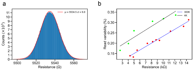
Measurements were conducted on the same sample at and room temperature using a Keysight B1500A semiconductor analyzer with a waveform generator module (WGFMU) coupled with a Lakeshore CRX-VF cryogenic probe station (see Fig. 2a and b). The TiO-based memristors were formed beforehand at . We demonstrate 11 distinct resistance states at and , with approximately 50 write pulses for each state with a programming accuracy of 1%. We observe that the resistance can decrease instead of increasing when applying negative write pulses during the multilevel programming. This phenomenon is more important at larger resistance values and can be defined as write variability. Cryogenic multilevel programming of the memristor (See Fig. 2b) shows a larger resistance decrease, which could be imputed to the larger temperature gradient in the vicinity of the conductive filament Strukov2012 . Moreover, at cryogenic temperatures, the competition between thermal- and field-activated effects is increased and could lead to additional variability during the thermally-activated RESET operation (increasing of the memristor resistance) Beilliard2020IOP ; Govoreanu_cryo_pulse . One can also note reading variability from the inset of Fig. 2a and b, which can be associated with thermal noise induced by the memristor conduction modes. We evaluate a sub-1% read variability on our devices, which allows for precise and stable resistance states (see Supplementary Fig. 3 for the characterization of the reading variability). A better programming accuracy can be reached using a smaller voltage step for pulse amplitude at the cost of programming time (i.e., more write pulses). Finally, we simulated the multilevel programming of our TiO2-based memristors (See Fig. 2c) by fitting a Data-Driven model Messaris_data_driven replicating the pulsed response transient of a resistive memory (see Supplementary Fig. 2) for the fitting) that will enable the design of cryogenic memristor circuits. This model closely replicates the programming of the resistance states, which allows high-fidelity hardware-based simulations of the DC source in the following section.
V Simulations and discussions
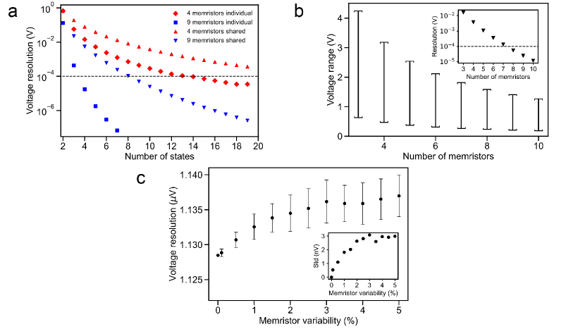
Using the Data-Driven memristor model Messaris_data_driven parameters fitted on our experimental data at , we will next benchmark the performance of the memristor-based DC source by varying the number of memristors in the circuit and the number of distinct resistance states. We initially consider the circuit with no read or write variability to assess the optimal voltage resolution and range achievable.
Figure 3a shows the evolution of the voltage resolution of the memristor-based DC source with respect to the number of states and the number of memristors. A higher number of resistance states leads to a better voltage resolution, which is limited by the maximum number of distinct resistance states achievable with the memristor used. By programming five states on nine memristors, we ideally reach a voltage resolution of , which is well below the target resolution required for QDs biasing. This five-states distribution is therefore used for the following simulations. Figure 3b specifies the basic electrical characteristics of the DC-source with respect to the number of memristors used. This figure shows the trade-off between the voltage resolution and the range as the number of memristors increases, this trend is explained by equations (1) and (2). For an increasing number of memristors, the voltage range decreases while the resolution increases exponentially. To comply with the voltage resolution and -range requirements for quantum dot biasing, a circuit of at least eight memristors is needed if the number of states is fixed to five, which eases the multilevel programming operation. In the remainder of this paper, we consider a nine-memristor circuit to utilize the denser and more common 33 memristor-crossbar footprint.
To properly evaluate the memristor-based DC electrical specifications, we investigated the impact of memristor non-idealities Adam2018 on the DC source output voltage. Figure 3c shows the voltage resolution of a nine-memristor five-state circuit with respect to the memristor variability. We chose the memristor variability as the combination of the read and write variabilities observed with our devices and implemented it as a percentage error of the resistance for each memristor. As this simulated memristor variability increases, the voltage resolution of the DC source remains almost constant. This suggests that the memristor’s variability has a negligible impact on the voltage resolution of the memristor-based DC source. We also note a decrease in the reproducibility of the constant step size between two consecutive output voltages (see inset of Fig. 3c). We can compare the averaged error induced by the memristor variability to the voltage noise of DC sources that are used in quantum dot setups, typically in the order of 1 to 5% of the target voltage (2.0% for the Tektronix 5014C).
The proposed DC source was programmed by reaching target resistance states for each memristor, leading to an associated output voltage. In the preceding simulations, we chose to consider the memristors as discrete multi-state resistors. This allowed for efficient programming because a simple feedback resistance algorithm can be used, as in Alibart2012 , to tune the whole crossbar array. Using this discrete programming approach, the output voltages depend on the resistance targets that we initially set, thus limiting our control of the output voltage. Instead, the memristor-based DC source can be controlled to reach an arbitrary target voltage to enable a more precise control of the PGA output voltage by exploiting the fully analog behaviour of the memristors. We propose a servo algorithm, which will program the memristor crossbar to reach the target voltage accordingly. The crossbar resistance configuration is chosen in a pre-computed dataset, where the keys are target output voltages. We converge towards this optimal resistance configuration by performing a first coarse round of programming for each memristor to roughly reach the attributed resistance using the feedback algorithm for multilevel programming (see Fig. 2a, b and c). During a second round of programming, the resistance of the last memristor of the crossbar is finely tuned with a smaller voltage step and programming tolerance to a new target resistance that is specifically computed to balance the programming inaccuracy of the initial fast programming made on the other memristors. This fine tuning method allows for memristor variability robustness and a constant step size within a 2.5% voltage error using a nine-memristor circuit. Controlling the memristor-based DC source to reach an arbitrary voltage offers a smaller voltage resolution when compared to the resistance-driven operation mode. However, the proposed memristor-based programmable DC source still satisfies the for the same circuit parameters—that is, nine memristors and a supply voltage —and is more suitable for in-situ use of the DC source.
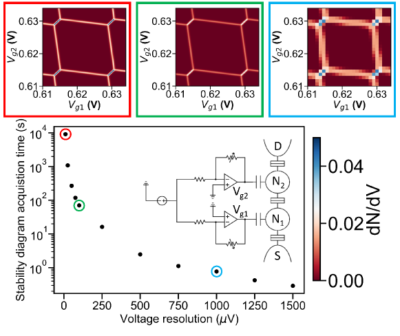
Now that we have explained the working principle of our memristor-based DC source and demonstrated how it can be operated to reach a target voltage, we will next simulate its co-integration with a double quantum dot to validate its compatibility with quantum systems. Stability diagrams are used as a standard benchmark measurement to verify the basic performance of a quantum dot system. We simulated the electron transport through a double quantum dot (DQD) with respect to the voltages applied to its gates while biased by two memristor-based cryogenic DC source using equations from VDW_QD_transport (see Methods). Two important metrics to consider for a QD biasing solution are the voltage resolution and the stability diagram acquisition time, which is estimated by counting the number of write and read pulses needed to program the memristor circuit during the simulation of the charge stability diagram. This acquisition time increases with better voltage resolution, leading to a trade-off between speed and accuracy (see Fig. 4). The insets of Figure 4 show the derivative of a charge stability diagram to highlight the transition between the electronic regimes of the simulated DQD. We can identify the transition and occupations of the DQD for the three voltage resolutions—that is, , and —, thus demonstrating the control of a simulated DQD by the proposed memristor-based DC source. Although the DC source can conveniently deliver voltage resolution from to below , a resolution is sufficient to clearly observe the honeycomb pattern and its triple-point. It also allows for a fast -scanning of the DQD stability diagram. Moreover, when scaling up the DC-sources for a large number of double quantum dots, the stability diagram measurement can be performed in parallel. This allows us to scan all double quantum dots within seconds using a resolution.
VI Conclusion
In conclusion, we propose a memristor-based cryogenic programmable DC source for scalable in-situ quantum-dot control. We demonstrate that this control approach fulfills the baseline requirements for quantum dot biasing (i.e., a -resolution over a range) while keeping a limited number of memristors, allowing for a scalable biasing solution. We demonstrated the effective biasing of a simulated double quantum dot using a non-ideal TiO2/Al2O3 memristor model, pointing out that memristor variability will not cause electronic regime changes that would be detrimental to quantum computation. We reported successful multilevel pulsed programming of TiO2-based memristor at . This demonstration is a first step towards more advanced cryogenic applications for resistive memories, such as cryogenic control electronics for quantum computers using this proposed in-situ memristor-based DC source.
Moreover, the scalability of this solution is limited by the total power dissipation of the DC source but still hints at a feasible integration of a few hundred of DC sources at , where the cooling power is on the order of a watt. More resistive memristors would allow us to decrease the power dissipation by limiting the current flowing in the feedback loop. Further works remain to be done regarding the thermal load introduced by memristors while they are being programmed to ensure cryo-compatibility. However, this additional heat load is limited to the bias tuning phase because memristors are non-volatile and the supply is maintained once programmed.Furthermore, the recent demonstrations of silicon spin qubits operated at temperatures above Yang2020 ; Petit2020 paves the way towards on-chip co-integration of ’hot’ quantum dots and memristor-based control electronics. This approach would allow us to overcome the wiring bottleneck that the community will face when scaling-up quantum computers.
Data availability
The code to control the Keysight B1500 that was used to perform the measurements is available at GitHub MounyB15002021 and the Python library that was developed to simulate the control performed by the proposed DC source is available at GitHub MounyQDMS2021 . The figures were created using Matplotlib Hunter_plt
Data supporting this work will be uploaded to an online repository.
Acknowledgements
This work was supported by Natural Sciences and Engineering Research Council of Canada (NSERC). This research was undertaken thanks in part to funding from the Canada First Research Excellence Fund. We acknowledge financial supports from the EU: ERC-2017-COG project IONOS (# GA 773228). We would like to acknowledge Christian Lupien, Edouard Pinsolle and the Institut Quantique for their assistance with the electrical characterisation at cryogenic temperatures. LN2 is French-Canadian joint International Research Laboratory (IRL-3463) funded and co-operated by CNRS, Université de Sherbrooke, Université de Grenoble Alpes (UGA), École Centrale Lyon (ECL) and INSA Lyon. It is supported by the Fonds de Recherche du Québec Nature et Technologie (FRQNT). We would also like to thank the IEMN cleanroom engineers for their support with the device fabrication.
Author contributions
P.A.M. and S.G. performed the experiment. A.E.M., R.D., P.G. and S.E. fabricated the memristor devices. P.A.M. analysed and post-processed the measurement and simulation data. P.A.M., S.G. and M.A.R. developed the simulation framework Y.B., D.D. and M.P.L. conceived and supervised the project. P.A.M. wrote the manuscript with input from all of the authors.
Competing interests
The authors declare no competing interests.
References
- [1] R. Pillarisetty, N. Thomas, H.C. George, K. Singh, J. Roberts, L. Lampert, P. Amin, T.F. Watson, G. Zheng, J. Torres, M. Metz, R. Kotlyar, P. Keys, J.M. Boter, J.P. Dehollain, G. Droulers, G. Eenink, R. Li, L. Massa, D. Sabbagh, N. Samkharadze, C. Volk, B. P. Wuetz, A.-M. Zwerver, M. Veldhorst, G. Scappucci, L.M.K. Vandersypen, and J.S. Clarke. Qubit device integration using advanced semiconductor manufacturing process technology. In 2018 IEEE International Electron Devices Meeting (IEDM), pages 6.3.1–6.3.4, 2018.
- [2] A. M. J. Zwerver, T. Krähenmann, T. F. Watson, L. Lampert, H. C. George, R. Pillarisetty, S. A. Bojarski, P. Amin, S. V. Amitonov, J. M. Boter, R. Caudillo, D. Corras-Serrano, J. P. Dehollain, G. Droulers, E. M. Henry, R. Kotlyar, M. Lodari, F. Luthi, D. J. Michalak, B. K. Mueller, S. Neyens, J. Roberts, N. Samkharadze, G. Zheng, O. K. Zietz, G. Scappucci, M. Veldhorst, L. M. K. Vandersypen, and J. S. Clarke. Qubits made by advanced semiconductor manufacturing, 2021.
- [3] M. Veldhorst, J. C. C. Hwang, C. H. Yang, A. W. Leenstra, B. de Ronde, J. P. Dehollain, J. T. Muhonen, F. E. Hudson, K. M. Itoh, A. Morello, and A. S. Dzurak. An addressable quantum dot qubit with fault-tolerant control-fidelity. Nature Nanotechnology, 9(12):981–985, October 2014.
- [4] Jun Yoneda, Kenta Takeda, Tomohiro Otsuka, Takashi Nakajima, Matthieu R. Delbecq, Giles Allison, Takumu Honda, Tetsuo Kodera, Shunri Oda, Yusuke Hoshi, Noritaka Usami, Kohei M. Itoh, and Seigo Tarucha. A quantum-dot spin qubit with coherence limited by charge noise and fidelity higher than 99.9%. Nature Nanotechnology, 13(2):102–106, December 2017.
- [5] T. F. Watson, S. G. J. Philips, E. Kawakami, D. R. Ward, P. Scarlino, M. Veldhorst, D. E. Savage, M. G. Lagally, Mark Friesen, S. N. Coppersmith, M. A. Eriksson, and L. M. K. Vandersypen. A programmable two-qubit quantum processor in silicon. Nature, 555(7698):633–637, February 2018.
- [6] D. M. Zajac, A. J. Sigillito, M. Russ, F. Borjans, J. M. Taylor, G. Burkard, and J. R. Petta. Resonantly driven CNOT gate for electron spins. Science, 359(6374):439–442, December 2017.
- [7] C. H. Yang, R. C. C. Leon, J. C. C. Hwang, A. Saraiva, T. Tanttu, W. Huang, J. Camirand Lemyre, K. W. Chan, K. Y. Tan, F. E. Hudson, K. M. Itoh, A. Morello, M. Pioro-Ladrière, A. Laucht, and A. S. Dzurak. Operation of a silicon quantum processor unit cell above one kelvin. Nature, 580(7803):350–354, April 2020.
- [8] L. Petit, H. G. J. Eenink, M. Russ, W. I. L. Lawrie, N. W. Hendrickx, S. G. J. Philips, J. S. Clarke, L. M. K. Vandersypen, and M. Veldhorst. Universal quantum logic in hot silicon qubits. Nature, 580(7803):355–359, April 2020.
- [9] L. Geck, A. Kruth, H. Bluhm, S. van Waasen, and S. Heinen. Control electronics for semiconductor spin qubits. Quantum Science and Technology, 5(1), 2019.
- [10] Joseph C. Bardin, Evan Jeffrey, Erik Lucero, Trent Huang, Sayan Das, Daniel Thomas Sank, Ofer Naaman, Anthony Edward Megrant, Rami Barends, Ted White, Marissa Giustina, Kevin J. Satzinger, Kunal Arya, Pedram Roushan, Benjamin Chiaro, Julian Kelly, Zijun Chen, Brian Burkett, Yu Chen, Andrew Dunsworth, Austin Fowler, Brooks Foxen, Craig Gidney, Rob Graff, Paul Klimov, Josh Mutus, Matthew J. McEwen, Matthew Neeley, Charles J. Neill, Chris Quintana, Amit Vainsencher, Hartmut Neven, and John Martinis. Design and characterization of a 28-nm bulk-cmos cryogenic quantum controller dissipating less than 2 mw at 3 k. IEEE Journal of Solid-State Circuits, 54(11):3043–3060, 2019.
- [11] L. M. K. Vandersypen, H. Bluhm, J. S. Clarke, A. S. Dzurak, R. Ishihara, A. Morello, D. J. Reilly, L. R. Schreiber, and M. Veldhorst. Interfacing spin qubits in quantum dots and donors—hot, dense, and coherent. npj Quantum Information, 3(1), September 2017.
- [12] Andrea Ruffino, Tsung-Yeh Yang, John Michniewicz, Yatao Peng, Edoardo Charbon, and Miguel Fernando Gonzalez-Zalba. A cryo-CMOS chip that integrates silicon quantum dots and multiplexed dispersive readout electronics. Nature Electronics, December 2021.
- [13] Xiao Xue, Bishnu Patra, Jeroen P. G. van Dijk, Nodar Samkharadze, Sushil Subramanian, Andrea Corna, Brian Paquelet Wuetz, Charles Jeon, Farhana Sheikh, Esdras Juarez-Hernandez, Brando Perez Esparza, Huzaifa Rampurawala, Brent Carlton, Surej Ravikumar, Carlos Nieva, Sungwon Kim, Hyung-Jin Lee, Amir Sammak, Giordano Scappucci, Menno Veldhorst, Fabio Sebastiano, Masoud Babaie, Stefano Pellerano, Edoardo Charbon, and Lieven M. K. Vandersypen. CMOS-based cryogenic control of silicon quantum circuits. Nature, 593(7858):205–210, May 2021.
- [14] S. J. Pauka, K. Das, R. Kalra, A. Moini, Y. Yang, M. Trainer, A. Bousquet, C. Cantaloube, N. Dick, G. C. Gardner, M. J. Manfra, and D. J. Reilly. A cryogenic CMOS chip for generating control signals for multiple qubits. Nature Electronics, 4(1):64–70, January 2021.
- [15] Y. Xu, F. K. Unseld, A. Corna, A. M. J. Zwerver, A. Sammak, D. Brousse, N. Samkharadze, S. V. Amitonov, M. Veldhorst, G. Scappucci, R. Ishihara, and L. M. K. Vandersypen. On-chip integration of si/sige-based quantum dots and switched-capacitor circuits. Applied Physics Letters, 117(14):144002, 2020.
- [16] L. Chua. Memristor: The missing circuit element. IEEE Transactions on Circuit Theory, 18(5):507–519, 1971.
- [17] D. Strukov, G. Snider, D. Stewart, and et al. The missing memristor found. Nature, 453:80–83, 2008.
- [18] Fabien Alibart, Ligang Gao, Brian D Hoskins, and Dmitri B Strukov. High precision tuning of state for memristive devices by adaptable variation-tolerant algorithm. Nanotechnology, 23(7):075201, January 2012.
- [19] Abdelouadoud El Mesoudy, Gwénaëlle Lamri, Raphaël Dawant, Javier Arias-Zapata, Pierre Gliech, Yann Beilliard, Serge Ecoffey, Andreas Ruediger, Fabien Alibart, and Dominique Drouin. Fully cmos-compatible passive tio2-based memristor crossbars for in-memory computing, 2021.
- [20] Yann LeCun, Yoshua Bengio, and Geoffrey Hinton. Deep learning. Nature, 521(7553):436–444, May 2015.
- [21] Amirali Amirsoleimani, Fabien Alibart, Victor Yon, Jianxiong Xu, M. Reza Pazhouhandeh, Serge Ecoffey, Yann Beilliard, Roman Genov, and Dominique Drouin. In-memory vector matrix multiplication in monolithic complementary metal–oxide–semiconductor-memristor integrated circuits: Design choices, challenges, and perspectives. Advanced Intelligent Systems, 2(11):2000115, August 2020.
- [22] Yann Beilliard, François Paquette, Frédéric Brousseau, Serge Ecoffey, Fabien Alibart, and Dominique Drouin. Investigation of resistive switching and transport mechanisms of al2o3/tio2-x memristors under cryogenic conditions (1.5 k). AIP Advances, 10(2):025305, 2020.
- [23] Runchen Fang, Wenhao Chen, Ligang Gao, Weijie Yu, and Shimeng Yu. Low-temperature characteristics of hfox-based resistive random access memory. IEEE Electron Device Letters, 36(6):567–569, 2015.
- [24] S Blonkowski and T Cabout. Bipolar resistive switching from liquid helium to room temperature. Journal of Physics D: Applied Physics, 48(34):345101, July 2015.
- [25] Matthew D. Pickett, Julien Borghetti, J. Joshua Yang, Gilberto Medeiros-Ribeiro, and R. Stanley Williams. Coexistence of memristance and negative differential resistance in a nanoscale metal-oxide-metal system. Advanced Materials, 23(15):1730–1733, 2011.
- [26] Ye Zhang, Ning Deng, Huaqiang Wu, Zhiping Yu, Jinyu Zhang, and He Qian. Metallic to hopping conduction transition in ta2o5-x/taoy resistive switching device. Applied Physics Letters, 105(6):063508, 2014.
- [27] H. S. Alagoz, K. H. Chow, and J. Jung. Low-temperature coexistence of memory and threshold switchings in pt/tiox/pt crossbar arrays. Applied Physics Letters, 114(16):163502, 2019.
- [28] V A Voronkovskii, V S Aliev, A K Gerasimova, and D R Islamov. Conduction mechanisms of TaN/HfO x /ni memristors. Materials Research Express, 6(7):076411, April 2019.
- [29] R. Maurand, X. Jehl, D. Kotekar-Patil, A. Corna, H. Bohuslavskyi, R. Laviéville, L. Hutin, S. Barraud, M. Vinet, M. Sanquer, and S. De Franceschi. A CMOS silicon spin qubit. Nature Communications, 7(1), November 2016.
- [30] Harald Homulle and Edoardo Charbon. Performance characterization of altera and xilinx 28 nm fpgas at cryogenic temperatures. In 2017 International Conference on Field Programmable Technology (ICFPT), pages 25–31, 2017.
- [31] L. Le Guevel, G. Billiot, B. Cardoso Paz, M. L. V. Tagliaferri, S. De Franceschi, R. Maurand, M. Cassé, M. Zurita, M. Sanquer, M. Vinet, X. Jehl, A. G. M. Jansen, and G. Pillonnet. Low-power transimpedance amplifier for cryogenic integration with quantum devices. 7(4):041407, December 2020.
- [32] J. E. Proctor, A. W. Smith, T. M. Jung, and S. I. Woods. High-gain cryogenic amplifier assembly employing a commercial CMOS operational amplifier. Review of Scientific Instruments, 86(7):073102, July 2015.
- [33] Ioannis Messaris, Alexander Serb, Spyros Stathopoulos, Ali Khiat, Spyridon Nikolaidis, and Themistoklis Prodromakis. A data-driven verilog-a reram model. IEEE Transactions on Computer-Aided Design of Integrated Circuits and Systems, 37(12):3151–3162, 2018.
- [34] Dmitri B. Strukov, Fabien Alibart, and R. Stanley Williams. Thermophoresis/diffusion as a plausible mechanism for unipolar resistive switching in metal–oxide–metal memristors. Applied Physics A, 107(3):509–518, March 2012.
- [35] Yann Beilliard, François Paquette, Frédéric Brousseau, Serge Ecoffey, Fabien Alibart, and Dominique Drouin. Conductive filament evolution dynamics revealed by cryogenic (1.5 k) multilevel switching of CMOS-compatible al2o3/TiO2 resistive memories. Nanotechnology, 31(44):445205, August 2020.
- [36] Bogdan Govoreanu, Sergiu Clima, Iuliana P. Radu, Yang-Yin Chen, Dirk J. Wouters, and Malgorzata Jurczak. Complementary role of field and temperature in triggering on/off switching mechanisms in <formula formulatype="inline"><tex notation="tex"></tex></formula> resistive ram cells. IEEE Transactions on Electron Devices, 60(8):2471–2478, 2013.
- [37] Gina C. Adam, Ali Khiat, and Themis Prodromakis. Challenges hindering memristive neuromorphic hardware from going mainstream. Nature Communications, 9(1), December 2018.
- [38] W. G. van der Wiel, S. De Franceschi, J. M. Elzerman, T. Fujisawa, S. Tarucha, and L. P. Kouwenhoven. Electron transport through double quantum dots. Reviews of Modern Physics, 75:1–22, Dec 2002.
- [39] P-A Mouny. B1530a control script. https://github.com/3it-nano/B1530A_control, 2021.
- [40] P-A Mouny and S. Graveline. Qdms: A quantum dot/memristor simulator. https://github.com/3it-nano/QDMS, 2021.
- [41] John D. Hunter. Matplotlib: A 2d graphics environment. Computing in Science Engineering, 9(3):90–95, 2007.
- [42] Hwang Jason Chun Chieh. Silicon MOS Quantum Dot Qubits for Spin-Based Quantum Computing. PhD thesis, University of New South Wales, 2018.
- [43] Emmanuel Chanrion, David J. Niegemann, Benoit Bertrand, Cameron Spence, Baptiste Jadot, Jing Li, Pierre-André Mortemousque, Louis Hutin, Romain Maurand, Xavier Jehl, Marc Sanquer, Silvano De Franceschi, Christopher Bäuerle, Franck Balestro, Yann-Michel Niquet, Maud Vinet, Tristan Meunier, and Matias Urdampilleta. Charge detection in an array of cmos quantum dots. Physical Review Applied, 14:024066, Aug 2020.
- [44] M. Rudolph, P. Harvey-Collard, R. Jock, T. Jacobson, J. Wendt, T. Pluym, J. Domínguez, G. Ten-Eyck, R. Manginell, M. P. Lilly, and M. S. Carroll. Coupling mos quantum dot and phosphorous donor qubit systems. In 2016 IEEE International Electron Devices Meeting (IEDM), pages 34.1.1–34.1.4, 2016.
- [45] Virginia N. Ciriano-Tejel, Michael A. Fogarty, Simon Schaal, Louis Hutin, Benoit Bertrand, Lisa Ibberson, M. Fernando Gonzalez-Zalba, Jing Li, Yann-Michel Niquet, Maud Vinet, and John J.L. Morton. Spin readout of a cmos quantum dot by gate reflectometry and spin-dependent tunneling. PRX Quantum, 2:010353, Mar 2021.
- [46] Zajac David. Single Electron Spin Qubits in Silicon Quantum Dots. PhD thesis, Princeton University, 2018.
Methods
Fabrication of a TiO-based memristor. The sample that was used for the measurements presented in this article followed our fabrication process of CMOS-compatible Al2O3/TiO2-x memristor devices described in [19], with two main differences: the TiO2 layer is thick, and the electrodes are wide.
Electrical characterizations All of the electrical characterizations were conducted on a Keysight B1500 using the WGFMUs module enabling the generation of the write pulses paired with a Lakeshore CRX-VF probe station allowing for measurements down to approximately . The WGFMUs are controlled using a GPIB-USB connection along with a custom C++ script based on a Keysigh library [39]. The script allows us to perform multilevel resistance programming, as well as the measurement required for the fitting of our simulation model.
Read variability assessments. The read variability of a memristor is measured by biasing the device at the voltage that is typically used for read pulse (i.e., ). The current flowing the through the memristor is measured every (sampling rate ) for because the B1500 analyzer is limited to a maximum of four MSamples. Each sample point is the result of an averaging over . This approach allows us to smoothen the read variability leading to a smaller standard deviation in the Gaussian fit, while replicating the action of a read pulse used in multilevel programming measurements. The experimental data can be fitted by a Gaussian to estimate the reading variability of the device. We conducted these measurements on the same memristor at room temperature and (see Supplementary Fig. 3). The coefficients extracted from the linear regression applied to the post-processed measurement data are used to complete our simulation model and implement variability to the emulated memristor.
Simulations.
The simulation framework was developed as a two parts (classical electronics and quantum) simulator. The classical simulations are based on Kirchhoff’s laws, the differential amplifier equation and the data driven model giving the memristor resistance with respect to the write pulse applied [33]. We added additional parameters to the data driven model to replicate basic non-idealities of the memristor, such as read and write variability, to more accurately predict the DC source behaviour. The quantum simulations are limited to the plotting of stability diagrams. We used the equations of the electron transport through a double quantum dot in reference [38] to determine the double quantum dot occupation with respect to the gate voltages ( and ) under the assumption of solely Coulomb blockade. The stability diagrams presented in this article are plotted by derivating the dot occupation with respect to both variables ( and ). The quantum simulation can be ran for different existing quantum dots. We used capacitance parameters from the University of New South Wales from reference [42] as a standard but implemented quantum dot parameters from other leading groups [13, 43, 44, 45, 46]. These parameters were extracted by post-processing available stability diagrams using electron transport equations. The quantum simulation is temperature-dependent, which allows for the simulation of hot silicon quantum dots [8, 7]. The memristor model can also be changed according to the working temperature, either at or at room temperature (all of the simulation results that are presented in this article used the memristor model).
| Parameter | Value | Unit |
|---|---|---|
| F | ||
| F | ||
| F | ||
| F | ||
| F | ||
| T | K |
| Parameter | Value |
|---|---|