First-principles study of the electronic and optical properties of HoW impurities in tungsten disulfide
Abstract
The electronic and optical properties of single-layer (SL) tungsten disulfide (WS2) in the presence of substitutional Holmium impurities (HoW) are studied. Although Ho is much larger than W, density functional theory (DFT) including spin-orbit coupling is used to show that Ho:SL WS2 is stable. The magnetic moment of the Ho impurity is found to be 4.75 using spin-dependent DFT. The optical selection rules identified in the optical spectrum match exactly the optical selection rules derived by means of group theory. The presence of neutral HoW impurities gives rise to localized impurity states (LIS) with f-orbital character in the band structure. Using the Kubo-Greenwood formula and Kohn-Sham orbitals we obtain atom-like sharp transitions in the in-plane and out-of-plane components of the susceptibility tensor, Im and Im. The optical resonances are in good agreement with experimental data.
I Introduction
Single-layer (SL) transition metal dichalcogenides (TMDs) are very attractive materials because of their special electronic and optical properties that enable lots of promising applications.[1, 2] Since SL TMDs are semiconductors with a direct band gap,[3, 4] they can be used to build transistors and optoelectronic devices. Since the band gap is in the visible regime, photodetectors and solar cells can be developed. Growth processes typically introduce defects and impurities in SL TMDs with profound effects on their electronic, optical, and magnetic properties.[5, 6, 7]
Over the past few years we have developed theoretical models based on density functional theory (DFT), tight-binding model, and 2D Dirac equation for the description of the electronic and optical properties of vacancy defects in TMDs,[8, 9, 10] which are naturally occurring during different growth processes, such as mechanical exfoliation (ME), chemical vapor deposition (CVD), and physical vapor deposition (PVD). A central result of our papers is that group theory can be used to derive strict selection rules for the optical transitions, which are in excellent agreement with the susceptibility calculated by means of the Kubo-Greenwood formula using the Kohn-Sham orbitals.
In our recent paper in Ref. 10 we performed DFT calculations and obtained the optical spectrum of SL WS2 in the presence of substitutional ErW atoms. Although we did not include the effect of spin-orbit coupling (SOC), we obtained good agreement with Bai et al.’s experiments on Er-doped MoS2 thin films using CVD growth[11] and wafer-scale layered Yb/Er co-doped WSe2.[12] Similar results have been found by López-Morales et al.[13] One of our motivations was to find out whether some of the LIS of Er lie within the band gap of SL WS2. We were able to show that this is indeed the case. The reason for our motivation is that LIS inside the band gap of a semiconductor can be potentially used as a qubit or a qudit for quantum information processing. Remarkably, TMDs with rare-earth atoms (REAs) exhibit the unique property of strong isolation of their electrons in the unfilled 4f shell by the surrounding d shell. This property leads generally to high quantum yields, atom-like narrow bandwidths for optical transitions, long lifetimes, long decoherence times, high photostability, and large Stokes shifts. This strong isolation of the 4f electrons makes them behave like electrons in a free atom. Therefore, it is not surprising that Ce3+ impurities in yttrium aluminium garnet (YAG) can reach long coherence times of ms.[14] By replacing YAG with the calcium tungstate CaWO4 as host material, it is possible to avoid the paramagnetic impurities of Y and substantially reduce the nuclear spin concentration without isotopic purification. Consequently, the Hahn echo experiment is able to achieve a long spin coherence time of ms for Er3+ impurities in CaWO4.[15] Thus, it is advantageous to identify host materials for REAs with low concentrations or even free of paramagnetic impurities and nuclear spins. We argue here that TMDs are good candidates for such host materials.
Here, following Ref. 10, we calculate the electronic and optical properties of HoW impurities in SL WS2. In particular, we find a peak at 2120 nm in the optical spectrum which is in good agreement with the characteristic wavelength of Ho observed in Ho:YAG lasers.[16, Ho_YAG_2, 17] Laser systems that operate in the 2 m range offer exceptional advantages for free space applications compared to conventional systems that operate at shorter wavelengths. This gives them a great market potential for the use in LIDAR and gas sensing systems and for direct optical communication applications. Besides, we find additional peaks in the optical spectrum of HoW:SL WS2, which are a direct consequence of the D3h symmetry of the HoW impurity and the interplay between the valley angular momentum (VAM), exciton angular momentum (EAM), and lattice angular momentum (LAM).[18]
The goal of this paper is to demonstrate the existence of localized Ho spin-orbit states inside the bandgap of WS2, the ultra-narrow optical transitions due to the atom-like f-orbital states of Ho, and the strict optical selection rules by means of a combination of ab-initio DFT calculations, the Kubo-Greenwood formula, and group theory including SOC.
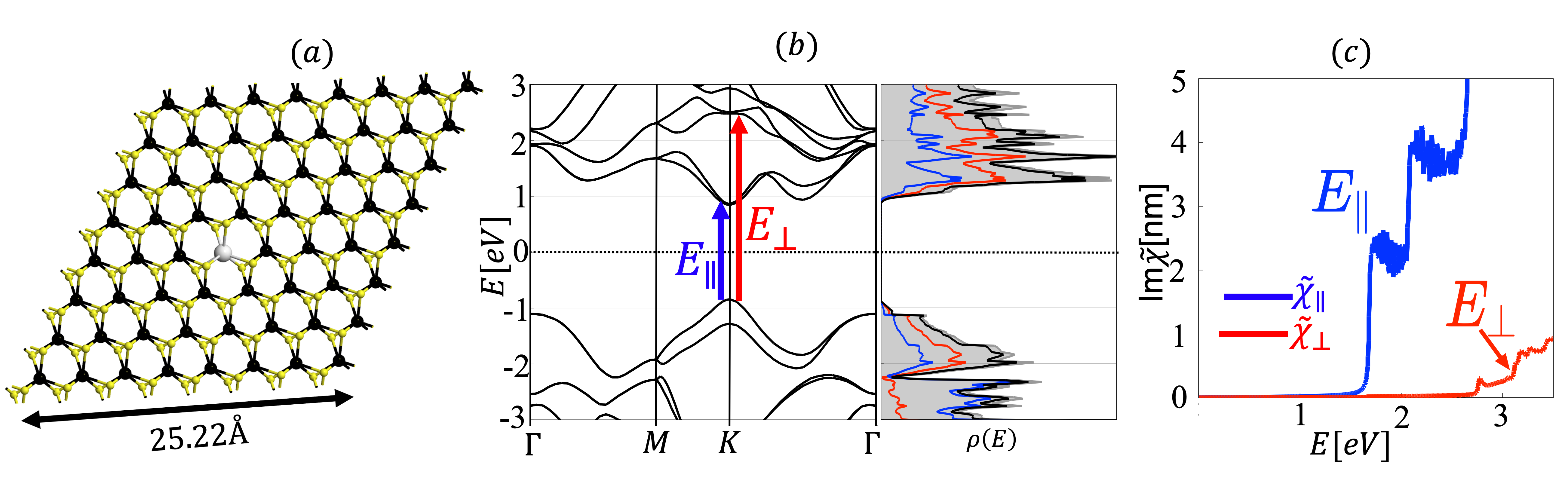
II Bandstructure
II.1 Numerical Analysis
All Numerical calculations are carried out by using DFT and with the use of Perdew–Burke–Ernzerhof (PBE) generalized gradient (GGA) parametrization[19] for exchange-correlation functional. Fully reletivistic noncollinear and spin polarized DFT calculations were performed as implemented in the Synopsis Atomistix Toolkit (ATK) 2021.06.[20]. For HoW impurity calculations, we consider a supercell consisting of eight unit cells along each crystalline-axis direction of the monolayer plane (i.e. 64 W atoms and 128 S atoms) and then replace a single W atom with Ho atom as shown in Fig. 1a). We consider a large supercell of edge length 25.22 Å, to fix the inter-impurity interactions. The point group of WS2 with HoW defect is D3h. The periodic structure of the superlattice allows one to characterize the electron states by the bandstructure , where is the vector in the first Brillouin zone of the superlattice and enumerates different bands. The sampling of the Brillouin zone was done for a supercell with the equivalent of a 32321 Monkhorst–Pack k-point grid for the WS2 primitive unit cell with a cutoff energy of 400 Ry. For all calculations, structure is first geometrically optimized with a force tolerance of 0.05 eV/Å. The formation energy for the HoW impurity is calculated by means of the relation
| (1) |
and are the total energy of the system with and without the impurity, respectively, is the number of added or removed species of atoms during the formation of the impurity. ’s are chemical potentials of the W and Ho atoms, which are estimated from their corresponding bulk forms. The small value of the formation energy eV indicates that the HoW impurity in WS2 is thermally stable.
We first obtain the results for bandstructure and electric susceptibility for pristine WS2 as shown in Fig. 1 b) and c), values of the band gap (1.64 eV) and splitting of the valence band edge (425 meV) due to SOC, are in good agreement with previously reported values.[21, 22, 23, 24] The crystal structure of SL WS2 is three atoms thin, where W atom is sandwiched in between two S atoms (S-W-S) via strong covalent bonds. Pristine SL WS2 is invariant with respect to reflection about the z = 0 (W) plane, where the zaxis is oriented perpendicular to the W plane of atoms. Therefore, electron states break down into two classes: even and odd, or symmetric and antisymmetric with respect to . -orbitals of the W and - orbitals ( and denoting the top and bottom layers) of the S atoms give the largest contribution to the conduction and valence band structure of SL WS2. [23, 25] Based on the symmetry, the even and odd atomic orbitals are spanned by the bases and , respectively.
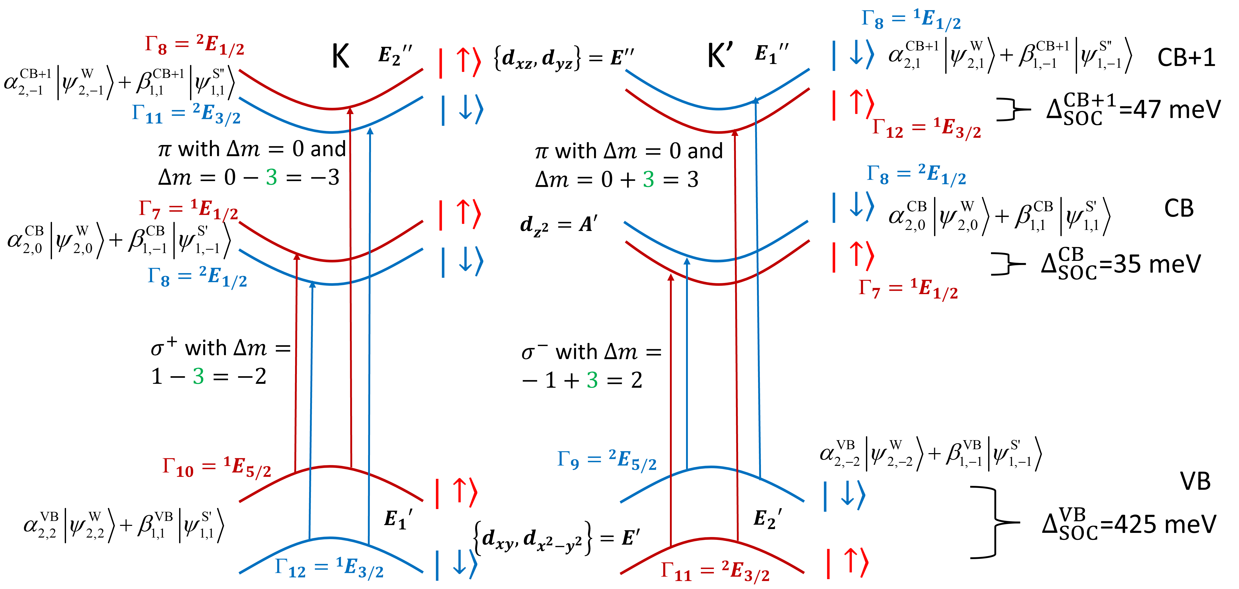
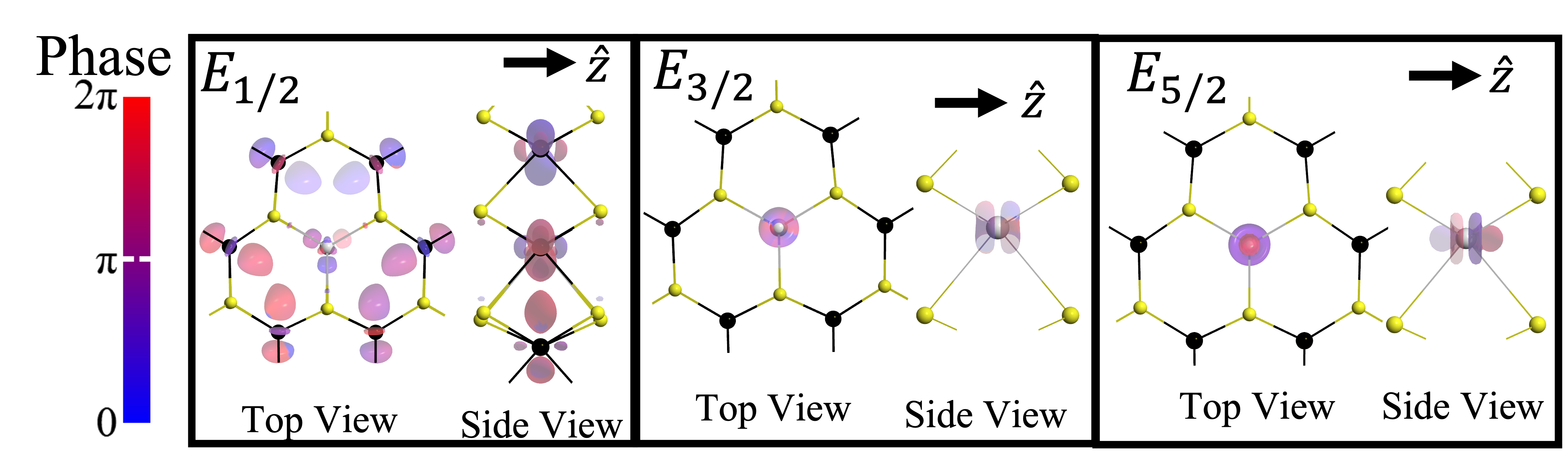
Using first principle studies[21, 22, 23], it is known that valence and conduction bands are primarily made from , and of W atoms, which transform as E, E and A′ irreducible representations (IRs) of the C3h symmetry group at the K and K’ points, in the absence of SOC (Table 2). The presence of SOC couples the spin and orbital angular momenta, thereby requiring the consideration of the double-group IRs. Double-group IRs can be obtained by multiplying single-group IRs with as shown in Table 1, where is the 2D spin representation. The spin-orbit states for pristine SL WS2 are shown in Fig. 5.
| linear | quadratic | ||||||||
| 1 | 1 | 1 | 1 | 1 | 1 | , | |||
| 1 | 1 | 1 | 1 | 1 | 1 | ||||
| 1 | 1 | ||||||||
| 1 | 1 | ||||||||
| 1 | 1 | ||||||||
| 1 | 1 | ||||||||
| 1 | |||||||||
| 1 | |||||||||
| 1 | |||||||||
| 1 | |||||||||
| 1 | |||||||||
| 1 | |||||||||
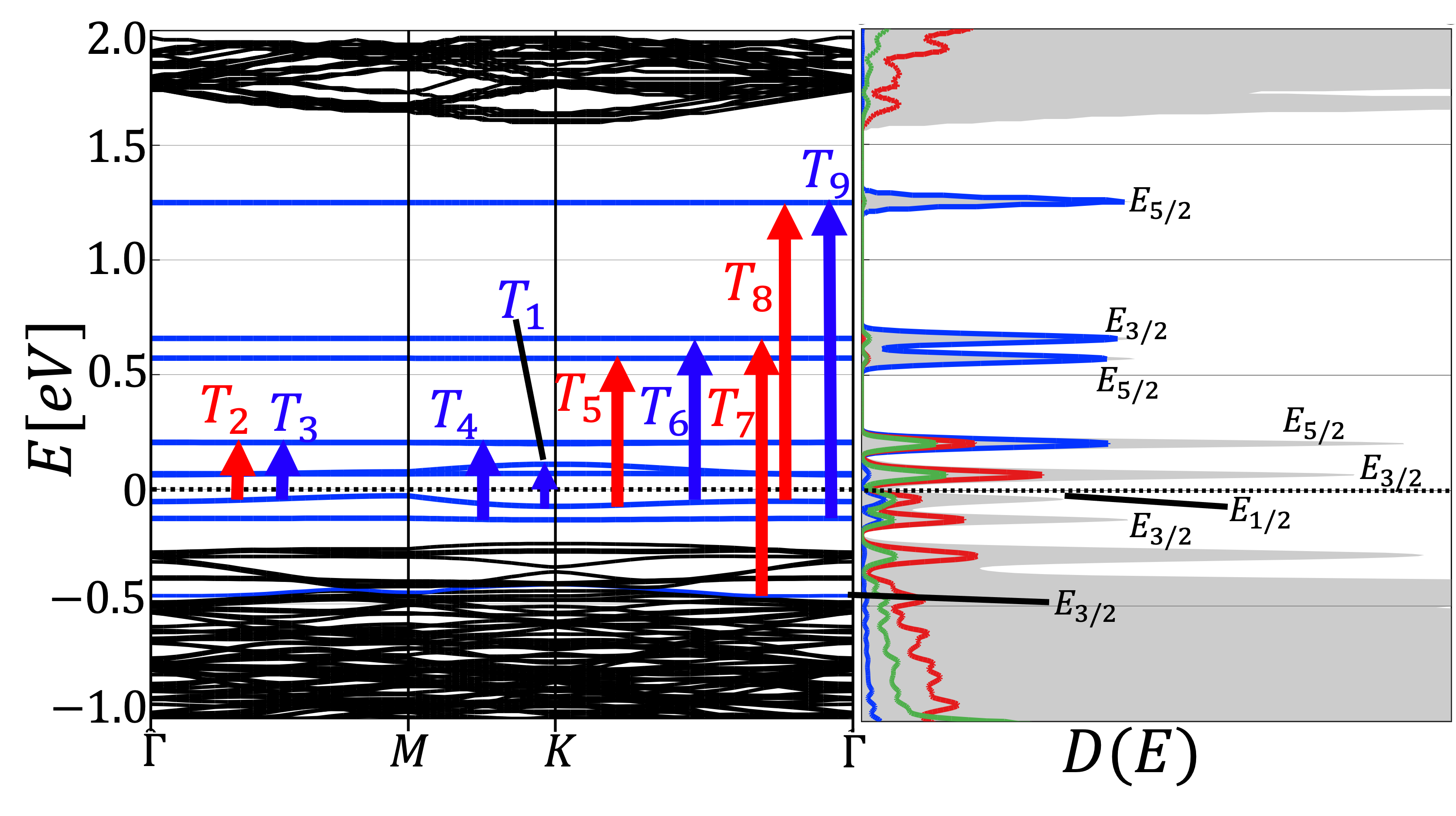
The bandstructure of WS2 with HoW impurities is shown in Fig. 2. Regular electronic states within the valence or conduction bands are depicted by black lines while LIS (orbitals of Ho) are depicted by blue lines. Some of the allowed optical transitions between different orbitals of Ho are depicted by vertical arrows. The resulting optical spectrum is shown in Fig. 7.
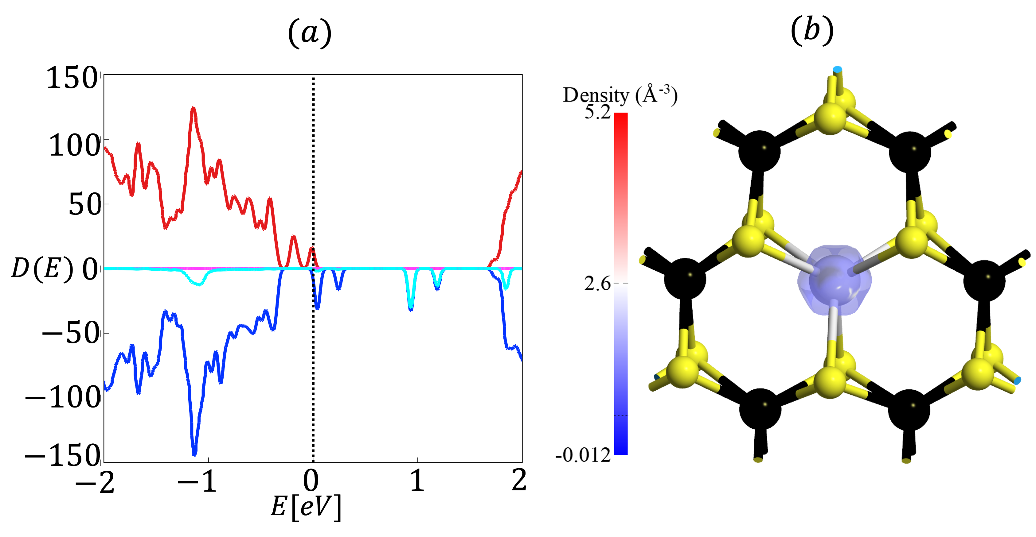
The Kramers theorem states that for every energy eigenstate of a time-reversal symmetric system with half-integer total spin, there is at least one more eigenstate with the same energy. In other words, every energy level is at least doubly degenerate if it has half-integer spin. It can be seen that Kramers degeneracy, which is a consequence of time reversal symmetry, is broken for LIS in HoW:SL WS2. In Ref. 26 it has been shown that presence of HoMo impurity leads to spin polarization and results in long range ferromagnetic coupling between local spins. The local magnetic moment of the HoW impurity breaks the time reversal symmetry and lifts the Kramers degeneracy. In order to confirm that indeed the HoW impurity in SL WS2 contains a magnetic moment, DFT calculations are performed by using spin-polarized GGA method. The results are presented in Fig. 3, where we show that the Ho impurity has a magnetic moment of 4.75. Our spin-polarized DFT calculations show that the exchange correlation potential leads to a spin splitting for HoW:SL WS2. In Fig. 3 (b) the isosurface plot for spin density shows that the main contribution to the magnetism is due to the orbitals of Ho atom while the bulk states do not show any magnetic moment, in contrast to what has been observed in Ref. 26, where a long-range magnetic interaction is seen. The reason is that we consider a much larger supercell of , as opposed to their supercell, resulting in a dilution of the impurity concentration that suppresses long-range magnetic interaction.
| linear | quadratic | ||||||||
| 1 | 1 | 1 | 1 | 1 | 1 | , | |||
| 1 | 1 | 1 | 1 | 1 | 1 | ||||
| 1 | 1 | 1 | 1 | 1 | 1 | ||||
| 1 | 1 | 1 | 1 | 1 | 1 | z | |||
| 2 | 2 | 1 | 1 | 0 | 0 | ||||
| 2 | 2 | 1 | 1 | 0 | 0 | ||||
| 0 | 0 | 0 | |||||||
| 0 | 0 | 0 | 0 | ||||||
| 0 | 0 | 0 | |||||||
II.2 Molecular Orbital Theory
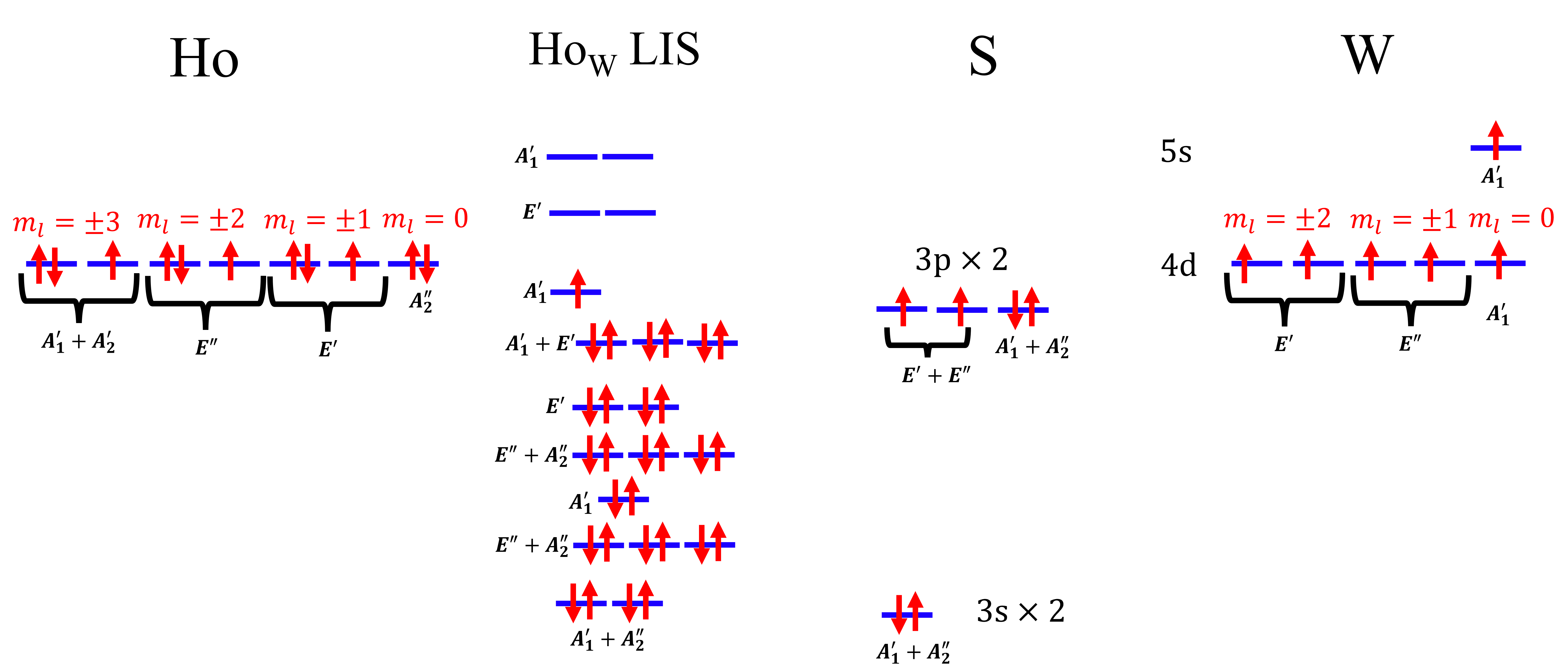
A HoW impurity inside WS2 looks similar to an atom in an effective electrostatic ligand field created by its neighboring six sulphur atoms. In this approximation molecular orbital theory (MOT) can be used. To identify the LIS in the DOS, the projected density of states (PDOS) showing orbital contributions of individual atoms is shown in Fig. 2. In addition to the contribution from the orbitals of HoW, contributions from the orbitals of the nearest neighboring S atoms and from the orbitals of next-nearest neighboring W atoms are present. This means that in the Hilbert base spanned by , an LIS state can be represented by
| (2) |
where the real coefficients ’s can be extracted from the PDOS shown in Fig. 2. Since admixture of orbitals is only allowed if they belong to the same IR, many coefficients are zero. The MOT diagram of pristine WS2 can be found in Ref. 10. The resulting eigenstates, identified by their IRs of , match the continuum states of the bands in WS2, as can be seen from Ref. 27.
Analyzing the PDOS, it becomes obvious that the Ho orbitals couple to both the orbitals of nearest neighboring S atoms and orbitals of next-nearest neighboring W atoms. The resulting MOT diagram including Ho LIS is shown in Fig. 4. The orbital energy ordering can be determined by comparison with the PDOS shown in Fig. 2. The highest occupied molecular orbital (HOMO) is a spin-orbit state with an orbital singlet state. The lowest unoccupied molecular orbital (LUMO) is a spin-orbit state with a orbital doublet state, which matches the PDOS in Fig. 2. Although the Ho atom with an average atomic radius of 1.75 Å is substantially larger than a W atom with an average atomic radius of 1.35 Å, DFT shows that the HoW impurity is stable in the WS2 host crystal. Because of the strong lattice distortions there are relatively strong hybridizations between the Ho orbitals and the W orbitals, as can be seen in the bandstructure in Fig. 2.
III Optical Response
Since the f-orbital contribution to the LIS is large, the optical spectrum exhibits narrow peaks, reminding of atom-like optical transitions. The relative dielectric functions of various TMDs have been measured in Ref. 28. We evaluate the matrix elements of the dielectric tensor in three dimensions () using the Kubo–Greenwood formula for the electric susceptibility
| (3) |
where is the dipole matrix element between Bloch states and , the volume of the crystal, the Fermi function, and eV the broadening. A vacuum separation of Å has been chosen in order to suppress not only electron bonding but also electrostatic interactions. In this limit the Bloch functions are localized on SL WS2. Consequently, we can use the approximation , where is the surface area of SL WS2. In this case , which has the unit of length, is independent of the vacuum separation. Using this definition, we present the in plane and out of plane components of the 3D susceptibility tensor for HoW impurities in SL WS2 in Fig. 7. We focus on transitions between states near the conduction and valence band edges and inside the band gap with resonance frequency , where is the eigenenergy of the Bloch state .
For pristine SL WS2 the point group symmetry at the K and K’ points is . A general result from group theory states that an optical transition is allowed by symmetry only if the direct product contains in its decomposition in terms of a direct sum. denotes the IR for the identity, i.e., for . The in plane and out of plane components of must be considered individually because they transform according to different IRs of the point group. The resulting optical selection rules are shown in Fig. 5. These selection rules corroborate the difference between the in-plane and out-of-plane band gaps and , respectively, which can be seen in the in-plane and out-of-plane susceptibilities Im and Im, respectively [see Fig. 1]. We predicted this difference in Refs. 8, 9, which has later been experimentally confirmed.[29] This difference has also been verified theoretically by means of DFT calculations with GW correction and the solution of the Bethe-Salpeter equation for in-plane and out-of-plane excitons.[30]
Alternatively, it is possible to use the conservation of angular momentum to derive the optical selection rules. In pristine SL WS2 the rotational symmetry relaxes the atomic optical selection rules for transitions and for transitions to for transitions and for transitions, whereby an angular momentum mismatch of can be transferred to or from the crystal lattice. The resulting optical selection rules match the ones obtained above from group theory and are also shown in Fig. 5. When using the approximation of a two-band model described by a Dirac Hamiltonian for the conduction (CB) and valence (VB) bands, our selection rules match the ones shown in Ref. 31.
Given the point group symmetry of impurities in a crystal, the LIS transform according to its IRs. In the case of the HoW impurity the point group symmetry is , its character table shown in Table 2. The identity for is . Table 5 shows the the selection rules for electric dipole transitions for the IRs. Note that the electromagnetic field couples only to the orbital part of the Bloch states. Therefore the we need to consider only the orbital IRs of . Remarkably, we show in Table 6 that several optical transitions are in good agreement with available experimental data for optical transitions in Ho3+:YAG.
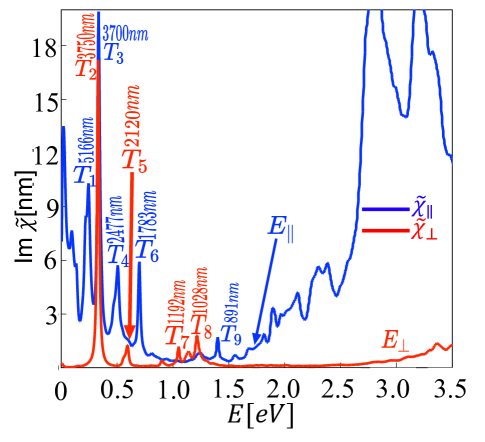
| Ho3+ states | Ho3+:YAG | Ho3+:WS2 | ||
|---|---|---|---|---|
| 5I 5I5 | 5.1 m () | |||
| 5I 5I6 | 3.75 m () or 3.70 m () | |||
| 5I 5I7 | 2.47 m () | |||
| 5I 5I8 |
|
2.12 m () or 1.78 m () | ||
| 5I 5I8 | 1.169 m [17] | 1.19 m () or 1.10 m () | ||
| 5I 5I8 | 899 nm [17] | 891 nm () |
IV Conclusion
Our results of electronic and optical properties of HoW impurities in SL WS2 reveal LIS inside and near the band gap and atom-like sharp optical transitions both in and . Therefore, we argue that REAs in TMDs are good candidate for spin qubits. Let us elaborate further.
Atom-like sharp optical transitions suggest that the decoherence time should be very long, which is one of the main criteria for a spin qubit. As mentioned in the introduction, by choosing a host material free of paramagnetic impurities and nuclear spins, it would be possible to substantially increase the spin coherence time of the impurity spin, in this case the spin of a HoW impurity. Therefore, let us compare rare-earth atom spins in TMDs with other currently existing solid-state spin qubits:
-
•
W has a weak abundance of 14% of nuclear spin ½ (183W) and S has a negligibly small abundance of 0.8% of nuclear spin 3/2 (33S). These can be removed by isotopic purification. In stark contrast to that, electron spin qubits in quantum dots made of GaAs suffer from hyperfine interaction. The issue is that Ga and As cannot be isotopically purified because all naturally abundant Ga and As isotopes have nuclear spins. Comparing to NV centers in diamond, N has a 99.6% abundance of nuclear spin 1 (14N) and 0.4% of nuclear spin 1/2 (15N). Therefore the nuclear spins of nitrogen cannot be removed by isotopic purification, either. In addition, P1 N impurities and surface spins are paramagnetic impurities that also lead to decoherence of an NV qubit. Consequently, we expect a much weaker decoherence of the Ho spin state.
-
•
The location in the direction perpendicular to the plane of the 2D material of the rare-earth impurities is accurate on the atomic level. By contrast, in 3D materials, such as GaAs and diamond, impurities and defects are spread throughout the 3D materials. Therefore we expect enhanced quantum sensing due to accurate distance to target atoms.
-
•
2D materials have clean surfaces, in stark contrast to diamond that hosts dark P1 nitrogen impurities with nuclear spins and surface spins. The spin coherence time of shallow NV centers in diamond within 30 nm of the surface degrades drastically due to increased electric and magnetic noise. Diamond surfaces are difficult to be etched and polished in a controlled way due to diamond’s hardness. [32]
Ce3+ in YAG exhibits electronic decoherence times of ms under dynamic decoupling [14]. This is relatively long considering that 27Al, the only naturally occurring isotope, has a nuclear spin of 5/2. Liu et al. have recently performed the Deutsch-Jozsa quantum algorithm on the electron spin of a Ce3+ ion in YAG by means of phase gates with an operation time of s.[33] This would allow for quantum operations. In the case of Er3+ impurities in CaWO4, the spin coherence time is ms, without isotopic purification.[15] In principle, this would allow for quantum operations.
Since WS2 can be isotopically purified to have zero nuclear spin, we expect even longer decoherence times and better performance with REAs in TMDs.
These advantages suggest that REAs embedded in 2D materials made of TMDs might be vastly superior to GaAs spin qubits and NV centers in diamond and could pave the way to realizing scalable quantum networks, scalable quantum computing, and ultrasensitive remote quantum sensing.
V References
References
- Wang et al. [2012] Q. H. Wang, K. Kalantar-Zadeh, A. Kis, J. N. Coleman, and M. S. Strano, Nat Nano 7, 699 (2012).
- Mak and AU Shan [2016] K. F. Mak and J. AU Shan, Nat Photon 10, 216 (2016).
- Mak et al. [2010] K. F. Mak, C. Lee, J. Hone, J. Shan, and T. F. Heinz, Phys. Rev. Lett. 105, 136805 (2010).
- Splendiani et al. [2010] A. Splendiani, L. Sun, Y. Zhang, T. Li, J. Kim, C.-Y. Chim, G. Galli, and F. Wang, Nano Letters 10, 1271 (2010).
- Liu et al. [2013a] D. Liu, Y. Guo, L. Fang, and J. Robertson, Applied Physics Letters 103, 183113 (2013a).
- Zhang and Li [2015] X. Zhang and Q. Li, Journal of Applied Physics 118, 064306 (2015).
- Banhart et al. [2011] F. Banhart, J. Kotakoski, and A. V. Krasheninnikov, ACS Nano 5, 26 (2011).
- Erementchouk et al. [2015] M. Erementchouk, M. A. Khan, and M. N. Leuenberger, Phys. Rev. B 92, 121401 (2015).
- Khan et al. [2017] M. A. Khan, M. Erementchouk, J. Hendrickson, and M. N. Leuenberger, Phys. Rev. B 95, 245435 (2017).
- Khan and Leuenberger [2021] M. A. Khan and M. N. Leuenberger, Journal of Applied Physics 130, 115104 (2021).
- Bai et al. [2016] G. Bai, S. Yuan, Y. Zhao, Z. Yang, S. Y. Choi, Y. Chai, S. F. Yu, S. P. Lau, and J. Hao, Advanced Materials 28, 7472 (2016).
- Bai et al. [2018] G. Bai, Z. Yang, H. Lin, W. Jie, and J. Hao, Nanoscale 10, 9261 (2018).
- López-Morales et al. [2021] G. I. López-Morales, A. Hampel, G. E. López, V. M. Menon, J. Flick, and C. A. Meriles, Computational Materials Science , 111041 (2021).
- Siyushev et al. [2014] P. Siyushev, K. Xia, R. Reuter, M. Jamali, N. Zhao, N. Yang, C. Duan, N. Kukharchyk, A. D. Wieck, R. Kolesov, and J. Wrachtrup, Nature Communications 5, 3895 (2014).
- Dantec et al. [2021] M. L. Dantec, M. Rančić, S. Lin, E. Billaud, V. Ranjan, D. Flanigan, S. Bertaina, T. Chanelière, P. Goldner, A. Erb, R. B. Liu, D. Estève, D. Vion, E. Flurin, and P. Bertet, Science Advances 7, eabj9786 (2021), https://www.science.org/doi/pdf/10.1126/sciadv.abj9786 .
- So et al. [2006] S. So, J. I. Mackenzie, D. P. Shepherd, W. A. Clarkson, J. G. Betterton, E. K. Gorton, and J. A. C. Terry, Opt. Express 14, 10481 (2006).
- Malinowski et al. [2000] M. Malinowski, Z. Frukacz, M. Szuflińska, A. Wnuk, and M. Kaczkan, Journal of Alloys and Compounds 300-301, 389 (2000).
- Xiao et al. [2015] J. Xiao, Z. Ye, Y. Wang, H. Zhu, Y. Wang, and X. Zhang, Light: Science & Applications 4, e366 (2015).
- Perdew and Zunger [1981] J. P. Perdew and A. Zunger, Phys. Rev. B 23, 5048 (1981).
- QW_[2019] http://www.quantumwise.com/ (2019).
- Xiao et al. [2012] D. Xiao, G.-B. Liu, W. Feng, X. Xu, and W. Yao, Phys. Rev. Lett. 108, 196802 (2012).
- Liu et al. [2013b] G.-B. Liu, W.-Y. Shan, Y. Yao, W. Yao, and D. Xiao, Phys. Rev. B 88, 085433 (2013b).
- Zhu et al. [2011] Z. Y. Zhu, Y. C. Cheng, and U. Schwingenschlögl, Phys. Rev. B 84, 153402 (2011).
- Zibouche et al. [2014] N. Zibouche, A. Kuc, J. Musfeldt, and T. Heine, Annalen der Physik 526, 395 (2014).
- Cappelluti et al. [2013] E. Cappelluti, R. Roldán, J. A. Silva-Guillén, P. Ordejón, and F. Guinea, Phys. Rev. B 88, 075409 (2013).
- Zhao et al. [2019] Q. Zhao, C. Zhai, Q. Lu, and M. Zhang, Phys. Chem. Chem. Phys. 21, 232 (2019).
- Pike et al. [2017] N. A. Pike, B. Van Troeye, A. Dewandre, G. Petretto, X. Gonze, G.-M. Rignanese, and M. J. Verstraete, Phys. Rev. B 95, 201106 (2017).
- Li et al. [2014] Y. Li, A. Chernikov, X. Zhang, A. Rigosi, H. M. Hill, A. M. van der Zande, D. A. Chenet, E.-M. Shih, J. Hone, and T. F. Heinz, Phys. Rev. B 90, 205422 (2014).
- Wang et al. [2017] G. Wang, C. Robert, M. M. Glazov, F. Cadiz, E. Courtade, T. Amand, D. Lagarde, T. Taniguchi, K. Watanabe, B. Urbaszek, and X. Marie, Phys. Rev. Lett. 119, 047401 (2017).
- Guilhon et al. [2019] I. Guilhon, M. Marques, L. K. Teles, M. Palummo, O. Pulci, S. Botti, and F. Bechstedt, Phys. Rev. B 99, 161201 (2019).
- [31] J. Xiao, Z. Ye, Y. Wang, H. Zhu, Y. Wang, and X. Zhang, Light: Science & Applications 4, e366.
- de Leon et al. [2021] N. P. de Leon, K. M. Itoh, D. Kim, K. K. Mehta, T. E. Northup, H. Paik, B. S. Palmer, N. Samarth, S. Sangtawesin, and D. W. Steuerman, Science 372, eabb2823 (2021).
- Liu et al. [2020] Z. Liu, Y.-X. Wang, Y.-H. Fang, S.-X. Qin, Z.-M. Wang, S.-D. Jiang, and S. Gao, National Science Review 7, 1557 (2020).