Ultrahigh Dynamic Range and Low Noise Figure Programmable Integrated Microwave Photonic Filter
Abstract
Microwave photonics (MWP) has adopted a number of important concepts and technologies over the recent pasts, including photonic integration, versatile programmability, and techniques for enhancing key radio frequency performance metrics such as the noise figure and the dynamic range. However, to date, these aspects have not been achieved simultaneously in a single circuit. Here, we demonstrate, for the first time, a multi-functional integrated microwave photonic circuit that enables on-chip programmable filtering functions while achieving record-high key radio frequency metrics of 120 dB.Hz dynamic range and 15 dB of noise figure that are previously unreachable. We unlock this unique feature by versatile complex spectrum tailoring using an all integrated modulation transformer and a double injection ring resonator as a multi-function optical filtering component. This work breaks the conventional and fragmented approach of integration, functionality and performance that currently prevents the adoption of integrated MWP systems in real applications.
Introduction
Integrated microwave photonic (MWP) systems can offer significant advantages in future radio frequency (RF) and microwave systems to realize advanced concepts such as multi-band, all-spectrum communications Akyildiz2020 and broadband programmable front-ends Chappell2014 , which are important for next generation communications (for example 6G). To play a key role in real RF applications, integrated MWP circuits need to simultaneously show advanced programmability and exceptional performance in terms of losses, noise figure, and dynamic range in a reduced footprint capmany2007microwave ; yao2009microwave ; capmany2012microwave ; marpaung2013integrated ; marpaung2019integrated . In recent pasts, a number of integrated MWP functions have widely been demonstrated, such as for filtering marpaung2013si ; shahnia2015independent ; fandino2017monolithic ; liu2020integrated ; tao2021hybrid , phase shifting li2011broadband ; burla2014onchip ; porzi2018photonic ; chew2019integrated ; mckay2019brillouin , delay line zhuang2011low ; liu2017gigahertz ; ji2019onchip ; tsokos2021silicon , waveform generator khan2010ultrabroad ; weiner2011ultrafast ; marpaung2011impulse ; wang2015reconfigurable ; zhu2020si ; falconi2022 and beamforming yi2011photonic ; yi2011photonic ; zhuang2014chip ; miller2020large ; zhu2020silicon . Typically, these functions were achieved in dedicated, or application specific circuits, and the measured RF metrics were only sparsely reported. The values of the RF gain, noise figure (NF), and spurious-free dynamic range (SFDR) in these circuits are usually far-off from the requirements of practical RF systems.
Recently, new ways of building a programmable integrated MWP circuit have been extensively explored, for example through mesh-waveguide circuits that can synthesize a large-number of functionalities through programming zhuang2015programmable ; perez2017multipurpose ; perez2020multipurpose ; bogaerts2020 . While versatile, the typical functional performance of these circuits, such as filter extinction, or passband quality, and the RF metrics were significantly lower than that of application specific circuits liu2017all ; liu2018link ; zhu2019positive ; daulay2021microwave . Thus, at present, the unique and well-sought combination of high integration-density, versatile programmability, and high RF performance remains elusive. In particular, there is a bottleneck in co-integrating components that support NF reduction and linearization with components that provide functionalities.
Achieving simultaneous on-chip programmability and high RF performance requires integration of new types of photonic devices. A versatile modulation transformer (MT) that can tailor the phases and amplitudes of optical carrier and RF sidebands has recently identified as a key element for enhancement of dynamic range guo2021versatile ; daulay2021tutorial ; liu2021integrated . On the other hand, a programmable resonator such as a double-injected ring resonator (DI-RR) cohen2018response can provide a large number of filtering functions in a device.
In this work, we experimentally demonstrate a programmable integrated MWP circuit with a unique combination of a versatile MT device and a DI-RR, realized in a low-loss silicon nitride platform. With this circuit, we show for the first time, an array of RF filtering functions simultaneously with record-low NF of 15 dB, achieved using low-biasing technique, and ultra-high dynamic range of 120 dB.Hz, achieved using on-chip linearization. Our results, point a significant step forward towards the realization of practical programmable integrated MWP circuit in a real life applications.
Results
Programmable Microwave Photonics
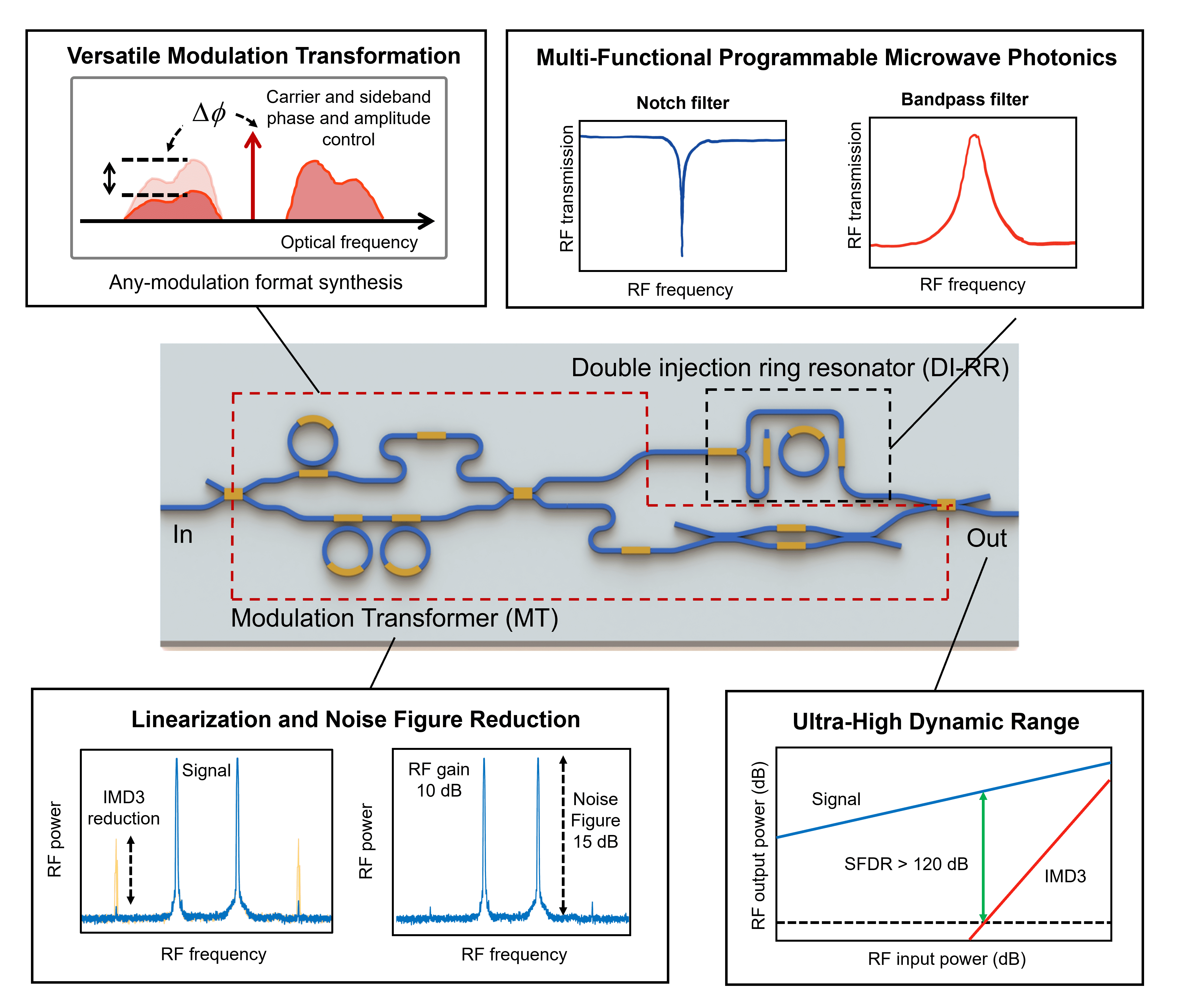
The concept of ultrahigh dynamic range and low NF programmable integrated MWP filter explored here is illustrated in Fig. 1. The MT shapes the input modulated signal from an optical modulator to a desired modulation format that suited the targeted filtering function. Further, the spectral shaping can be used to create bespoke optical carrier and sidebands phase and amplitude distribution leading to linearization and NF reduction. The DI-RR is used as a filtering element that can provide notch or bandpass filtering from the same output port. In this way, high dynamic range and programmable filtering can be achieved simultaneously.
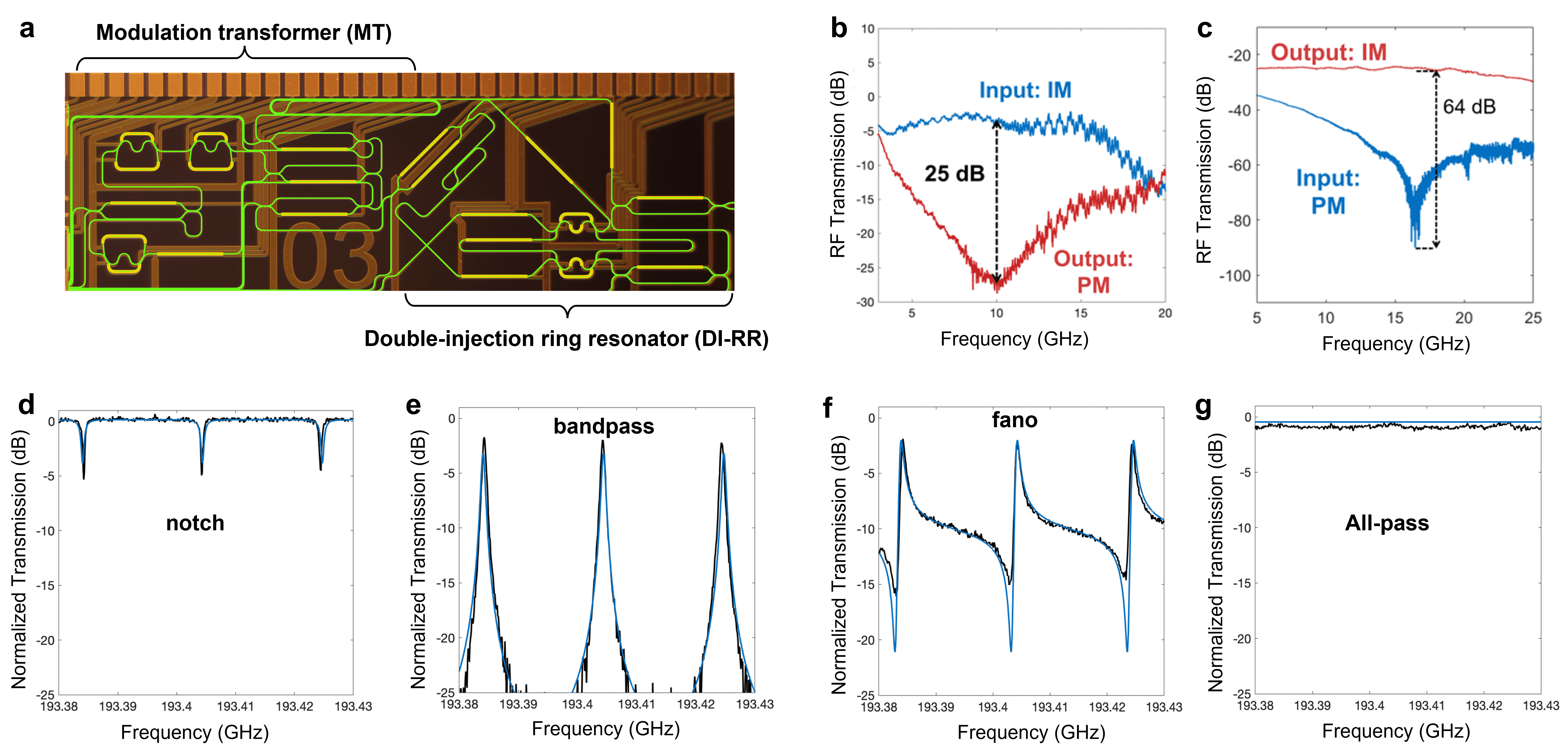
The MT is implemented as an asymmetric Mach-Zehnder interferometer (aMZI) loaded with 3 ring resonators as a spectral de-interleaver luo2010high ; guo2021versatile , combined with a tunable attenuator and a phase shifter (For the details of the MT, see Supplementary information A). The DI-RR is an add-drop ring resonator that is being double-injected from single input, hence capable of synthesizing a large number of responses (see Supplementary information B for the details of the DI-RR). The schematic of the entire circuit overlaid on a photograph of the fabricated silicon nitride chip is shown in Fig. 2a. The waveguide propagation loss in the circuit is 0.1 dB/cm, and the fiber-to-chip coupling loss is 1.1 dB/facet.
The programmability of our circuit is demonstrated by measurement results depicted in Fig. 2b-2g. An optical modulated spectrum at the input of the MT circuit can be transformed into an output spectrum consisting of spectral components with designer phase and amplitude profiles. As examples, when operated with intensity modulator input, our silicon nitride MT circuit is capable of intensity-to-phase modulation (IM-PM) conversion with 25 dB extinction (Fig. 2b), and with a phase modulator input, the circuit can achieve PM-IM conversion with 60 dB of extinction (Fig. 2c). The DI-RR, on the other hand, can synthesize a variety of responses from a single output port, including notch filter, bandpass filter, Fano-like response, and an all-pass response okky2021mwp as shown in Fig. 2d-2g. Because of the low propagation loss of the silicon nitride waveguide, narrow linewidth of the filtering function of around 400 MHz can be achieved in a device with 20 GHz free spectral range (FSR).
High Gain and Low Noise Figure MWP Filter
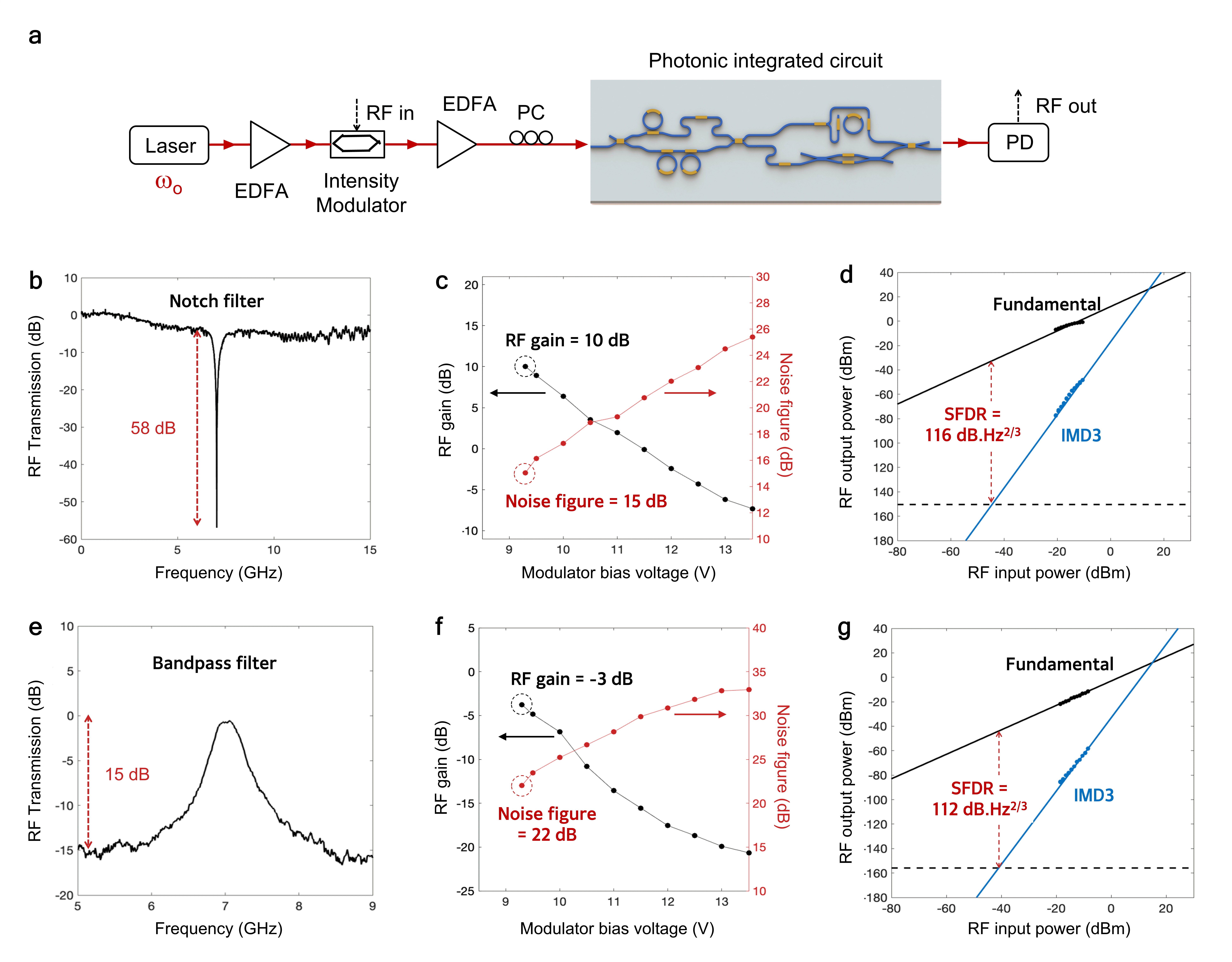
We carried out a series of MWP filtering experiments using our circuit, with a setup diagrammed in Fig. 3a. A high power optical source implemented with a external cavity laser and an erbium-doped fiber amplifier (EDFA) is sent to a low-biased IM, creating an intensity modulated spectrum. We then configure our MT to shape the IM spectrum into a dedicated output spectrum suitable for the filtering tasks provided by the DI-RR (see Supplementary information C for additional details of the extended experimental scenarios). In particular, we synthesized two RF filters with simultaneously high RF performance metrics. The first filter is an RF notch filter with intensity-to-asymmetric dual sidebands (IM-aDSB) modulation transformation using the MT and a notch response from the DI-RR. The second filter is an RF bandpass filter using combination of optical carrier re-insertion technique using the MT and a bandpass response from the DI-RR.
Figure 3b shows the measured RF notch filter with 58 dB rejection, 3-dB bandwidth of 400 MHz at the central frequency of 7 GHz. The high rejection in the filter was achieved through phase cancellation marpaung2015low enabled by adjusting the phase and amplitude of the isolated sideband in IM-aDSB modulation conversion. Through low biasing the IM, we then achieved an optimum measured RF gain of 10 dB and a lowest measured NF of 15 dB (Fig. 3c). These high gain and low noise figure translated into a high spurious-free dynamic range (SFDR) of 116 when we performed a two-tone test at the frequency of 1 GHz (Fig. 3d). These results represent the best RF gain, noise figure, and SFDR combination for an MWP notch filter. The RF notch filter central frequency can be tuned over 20 GHz, which is the full FSR of the DI-RR.
We then program the MT and the DI-RR to exhibit RF bandpass filter with 15 dB rejection, as shown in Fig. 3e. We measured RF gain of -3 dB, NF of 22 dB (Fig. 3f), and SFDR of 112 at 7 GHz (Fig. 3g). The versatility of the MT allows for the combination of low biasing and single-sideband (SSB)-based RF bandpass filtering, which would have not been possible only with an IM or a dual-parallel MZM. As a result, we can demonstrate the best combination of measured NF and SFDR for an RF bandpass filter. Importantly, these results were achieved without any electrical amplification in the system.
| Year | Technology | Type of | Number of | Type of | Tuning | Performance | Gain | Noise | SFDR |
| platform | devices | functions | functions | range | enhancement | figure | |||
| (GHz) | (dB) | (dB) | () | ||||||
| 2017 fandino2017monolithic | InP | Las., Mod., | 1 | LPF | 0-6 | No | -20 | N/A | 81.4 |
| RR, PD | |||||||||
| 2018 perez2017multipurpose | SOI | MZI mesh | 20 | BPF, notch | N/A | No | N/A | N/A | N/A |
| 2017 liu2017all | Si3N4 | RR | 1 | Notch | 0-12 | NF:LB | 8 | 15.6 | 116 |
| 2018 Zhang18OL | SOI | Mod., RR, PD | 1 | BPF | 3-10 | No | -39 | N/A | 92.4 |
| 2019 liu2019integrationbrillouin | As2S3 | RR, SBS | 1 | Notch | 0-15 | NF:LB | -10 | 27.1 | 96.5 |
| 2019 Zou19LPR | InP | Las., Mod., | 7 | BPF, notch | 8-15 | No | N/A | N/A | N/A |
| MMI | IFM, RFG | ||||||||
| 2020 Gertler20APL | SOI | SBS | 1 | BPF | 4-10 | No | -17 | 56.7 | 90.3 |
| 2020 daulay2020chip | Si3N4 | RR | 1 | BPF | 2-7 | NF:CS | -10 | 27 | N/A |
| 2021 daulay2021microwave | Si3N4 | RR | 1 | Notch | 3-10 | NF:CS | 3 | 31 | 100 |
| 2021 guo2021versatile | SOI | Mod., MT, | 2 | Notch, BPF | 5-25 | No | N/A | N/A | N/A |
| RR, PD | |||||||||
| 2021 tao2021hybrid | InP+SOI | Las., Mod., | 2 | Notch, BPF | 3-25 | No | -28 | 51 | 99.7 |
| RR, PD | |||||||||
| 2021 garret2021ultradeep | Si3N4+As2S3 | RR, SBS | 1 | Notch | 2-12 | No | N/A | N/A | 92.2 |
| 2021 Li2021OpeX | Si3N4+LiNbO3 | Mod., RR | 1 | Downconversion | 4-20 | No | -10 | 45 | 105 |
| (this work) | Si3N4 | MT, DI-RR | 6 | Notch, BPF | 4-20 | NF:LB | 10 | 15 | 116 |
| (this work) | Si3N4 | MT, DI-RR | 6 | Notch | 6-18 | SFDR:Lin. | -26 | 35 | 123 |
RR: ring resonator, PD: photodetector, Mod: modulator, MMI: multi-mode interference, SBS: stimulated Brillouin scattering, MT: modulation transformer, DI-RR: double-injection ring resonator, LPF: low pass filter, BPF: bandpass filter, IFM: instantaneous frequency measurement, PS: phase shifter, NF: noise figure, LB: low biasing, CS: carrier suppression, SFDR: spurious-free dynamic range, Lin: linearization.
On-Chip Linearization for Ultrahigh Dynamic Range
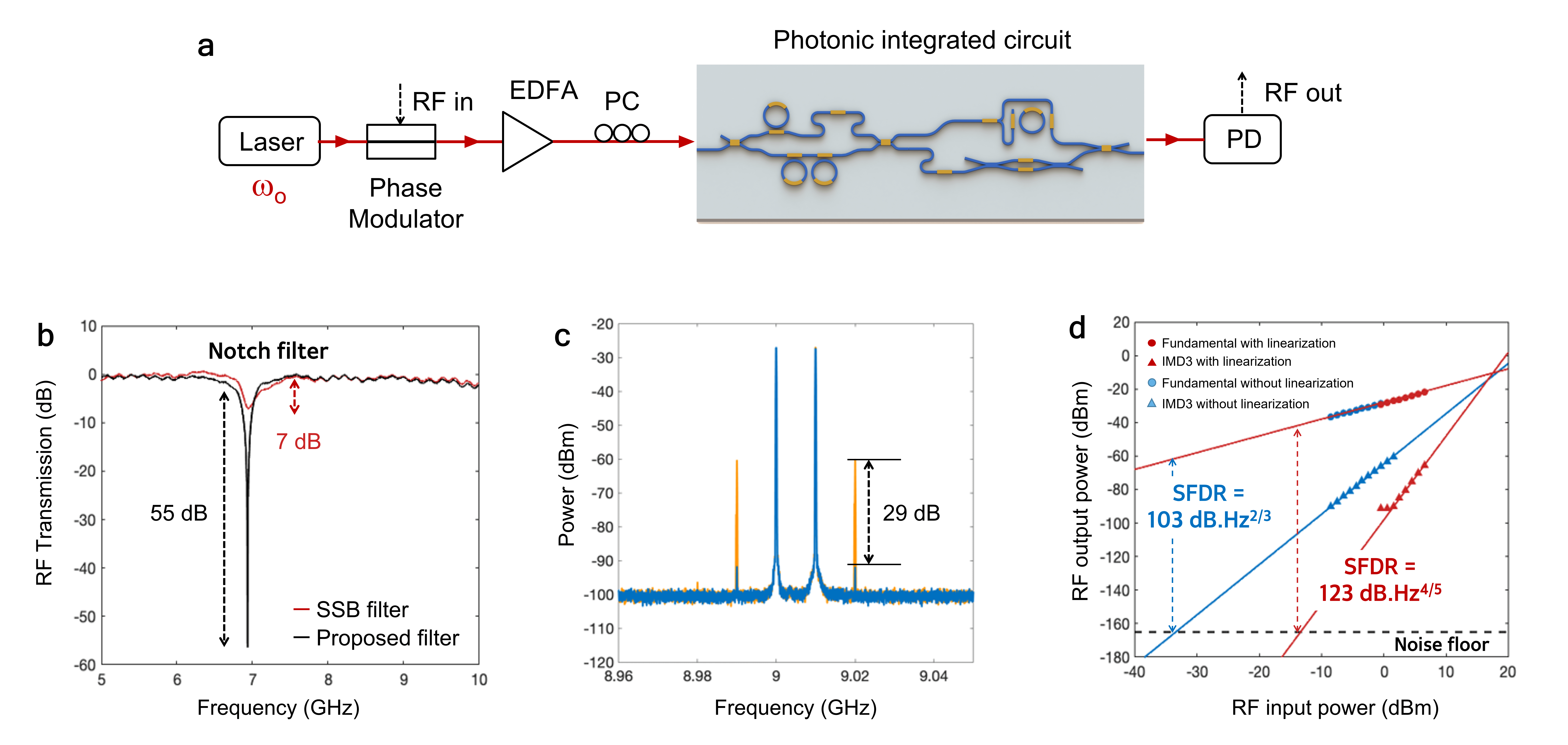
Some demanding applications of MWP require ultra-high SFDR beyond 120 dB.Hz marpaung2019integrated . Such a metric can be achieved through linearization of the modulator transfer function ZhangOoptica2016 ; ZhangOL20 ; MortonOE21 ; feng2022ultrahighlinearity . But achieving linearization simultaneously with functionalities has been proven challenging. Exploiting the versatility of our MT and DI-RR circuit, we demonstrate, for the first time, simultaneous RF notch filter and linearization in the same photonic chip.
Here, we implement third-order intermodulation distortion (IMD3) cancellation technique using complex multi-order sidebands spectral shaping as we previously reported liu2020linearized ; liu2021integrated ; liu2021simultaneous (see Supplmentary Notes D and E for the details of the linearization technique). In this experiment, light is sent to a phase modulator (PM) (Fig. 4a) that generates the optical carrier and first and higher order sidebands. The MT is used to convert the PM to aDSB modulation format, and to shape the amplitudes and phases of the first and second order sidebands yielding to IMD3 suppression. The DI-RR is then used to filter the first order sideband to create a phase cancellation RF notch filter. In this way, simultaneous RF notch filter and linearization can be achieved, leading to significant enhancement of the SFDR (For additional details of linearization theoretical analysis and working principle, see Supplementary information D and E respectively).
A conventional SSB RF notch filter without any linearization was used as a benchmark for the proposed linearized RF notch filter. Figure 4b shows the proposed linearized RF notch filter with 45 dB rejection improvement compared to the conventional SSB RF notch filter. With the linearization, we achieved 29 dB of IMD3 suppresion (Fig. 4c) and 20 dB SFDR improvement (Fig. 4d). With a noise floor of -164 dBm/Hz, the conventional SSB RF notch filter shows an SFDR of 103 , while the linearized RF notch filter exhibits a record-high SFDR of 123 . It is clear from the slope of the measured IMD3 powers that the fifth order distortion becomes the dominant factor due to cancellation of the third-order distortion. This result marked the highest SFDR simultaneously achieved with on-chip signal functionality.
Discussion
Table I summarizes the performance comparison of existing programmable MWP circuits reported in the past 5 years. The route to largest number of functions is still provided through MZI-mesh circuits perez2017multipurpose . Virtually all demonstrations, except the application specific RF notch filter reported in liu2017all , show relatively low RF performance, notably characterised by very high NF (25 dB) and low SFDR ( 100 dB.Hz). These results highlight the challenge in creating multifunctional and high-performance MWP circuit. Our results overcome this challenge by delivering high-level of reconfigurability with variety of functions in combination with high gain, low NF, and ultrahigh SFDR. Importantly, in the context of functional circuits, our demonstrations represent record-low NF and record-high SFDR to date.
At present, our approach enables NF reduction through low biasing of MZM intensity modulator. This translates into moderate SFDR enhancement as seen in Table I. Our linearization method, on the other hand, is working for PM-based MWP filter where maximum IMD3 suppression is achieved when the optical carrier is partially suppressed (See Supplementary Info D). Due to the limitation in maximum optical amplification in our experimental setup, the measured ultra-high SFDR is still accompanied by relatively low link gain and high NF (Table 1). Achieving the gain, NF, and SFDR advantages simultaneously is feasible in the PM link when higher optical amplification and higher power handling components are used. Alternatively. this can also be achieved by developing similar linearization strategy for low-biased MZM link.
In summary, we have designed, fabricated, and experimentally demonstrated, for the first time, programmable integrated MWP circuit based on a unique combination of versatile MT and equally versatile DI-RR. We reconfigure the circuit to synthesize an array of RF filtering functions with high RF gain, low NF, and ultrahigh SFDR concurrently. Hence, this work open a new paradigm and an important step forward towards the realization of programmable integrated MWP circuit with versatile functions, low NF, and ultra-high dynamic range for real life applications.
Methods
Silicon Nitride Circuit Fabrication
The waveguides in our circuit are fabricated using LioniX standard TriPleX Asymmetric Double-Stripe (ADS) geometry worhoff2015triplex ; roeloffzen2018low . First, a layer is grown from wet thermal oxidation of single-crystal silicon substrate with temperatures equal to or above 1000 ℃. Then, low-pressure chemical vapor deposition (LPCVD) is used for the Si3N4 layers and together with the gas tetraethylorthosilicate (TEOS) for intermediate SiO2 layer. Next, the waveguides are patterned using contact lithography, and processed with dry etching. Last, the waveguides are covered with an additional SiO2 layer through LPCVD TEOS. Because typical top cladding thickness cannot achieved only by LPCVD TEOS, plasma-enhanced chemical vapor deposition (PECVD) is used to increase the SiO2 top cladding thickness to a total of 8 µm. A thicker layers can be achieved because of the stress in PECVD SiO2 layers is much less than LPCVD layers.
Details of Programmable Microwave Photonics Experiments
An optical carrier from low relative-intensity noise (RIN) laser (Pure Photonics PPCL550) with RIN of -155 dB/Hz and wavelength set at 1550 nm is amplified with a low-noise erbium-doped fiber amplifier (EDFA, Amonics). Then, the output of amplified optical carrier is optically modulated using a MZM (Thorlabs, LN05S-FC 40 GHz) with bias point set at quadrature ( = /2). The MZM is driven by RF signal from a vector network analyzer (VNA, Keysight P5007A). The output of the MZM then sent to another low-noise EDFA (Amonics) before being injected into a programmable silicon nitride chip (LioniX International BV) fabricated using low-loss TriPleX (Si3N4/SiO2) technologyworhoff2015triplex ; roeloffzen2018low with propagation loss of the optical waveguide at 0.1 dB/cm. The chip can be tuned through thermo-optic tuning using custom made heater controller software, while being stabilized by a thermoelectric cooler (TEC) controller. The processed optical signal is sent to a photodetector (PD, APIC 40 GHz) and the converted RF signal is measured with a VNA, while the RF spectrum analyzer (RFSA, Keysight N9000B) is used to measure the RF filter’s noise and linearity.
Details of Linearization Experiments
A low RIN laser (Pure Photonics PPCL550) is modulated using a PM (EOSpace 20 GHz) using a sweeping RF signal with -3 dBm power from VNA (Keysight P5007A) for RF notch filter experiment. For the dynamic range experiment, the two-tone RF signal with power of 10 dBm, centered at 9 GHz with a space of 10 MHz from signal generators (Wiltron 69147A and Rohde-Schwarz SMP02) is used to drive the PM. The modulated signal is then amplified by a low-noise EDFA (Amonics), before coupling to a programmable silicon nitride chip (LioniX International BV). The processed optical spectrum is sent to a PD (APIC 40 GHz) to retrieve the RF signal and measured using the VNA for the filter’s response and the RFSA (Keysight N9000B) for linearity.
Author Contributions
O.D. and G.L. contributed equally in this work. O.D., G.L.,and D.M. developed the concept and proposed the physical system. O.D. designed the photonic circuits, O.D. and G.L. developed and performed numerical simulations. O.D. and G.L. performed the experiments with input from K.Y., R.B., and Y.K. E.K., M.H., and C.R. layout, developed, and fabricated the silicon nitride circuits. D.M., O.D. and G.L. wrote the manuscript with input from all authors. D.M. led and supervised the entire project.
Funding Information
This work was supported by Netherlands Organisation for Scientific Research NWO Vidi (15702) and NWO Start Up (740.018.021).
References
- (1) I. F. Akyildiz, A. Kak, and S. Nie, “6g and beyond: The future of wireless communications systems,” IEEE Access, vol. 8, pp. 133 995–134 030, 2020.
- (2) W. J. Chappell, E. J. Naglich, C. Maxey, and A. C. Guyette, “Putting the radio in “software-defined radio”: Hardware developments for adaptable rf systems,” Proceedings of the IEEE, vol. 102, no. 3, pp. 307–320, 2014.
- (3) J. Capmany and D. Novak, “Microwave photonics combines two worlds,” Nature photonics, vol. 1, no. 6, p. 319, 2007.
- (4) J. Yao, “Microwave photonics,” Journal of lightwave technology, vol. 27, no. 3, pp. 314–335, 2009.
- (5) J. Capmany, J. Mora, I. Gasulla et al., “Microwave photonic signal processing,” Journal of Lightwave Technology, vol. 31, no. 4, pp. 571–586, 2012.
- (6) D. Marpaung, C. Roeloffzen, R. Heideman et al., “Integrated microwave photonics,” Laser & Photonics Reviews, vol. 7, no. 4, pp. 506–538, 2013.
- (7) D. Marpaung, J. Yao, and J. Capmany, “Integrated microwave photonics,” Nature photonics, vol. 13, no. 2, pp. 80–90, 2019.
- (8) D. Marpaung, B. Morrison, R. Pant et al., “Si 3 n 4 ring resonator-based microwave photonic notch filter with an ultrahigh peak rejection,” Optics express, vol. 21, no. 20, pp. 23 286–23 294, 2013.
- (9) S. Shahnia, M. Pagani, B. Morrison, B. J. Eggleton, and D. Marpaung, “Independent manipulation of the phase and amplitude of optical sidebands in a highly-stable rf photonic filter,” Optics express, vol. 23, no. 18, pp. 23 278–23 286, 2015.
- (10) J. S. Fandiño, P. Muñoz, D. Doménech, and J. Capmany, “A monolithic integrated photonic microwave filter,” Nature Photonics, vol. 11, no. 2, pp. 124–129, 2017.
- (11) Y. Liu, A. Choudhary, D. Marpaung, and B. J. Eggleton, “Integrated microwave photonic filters,” Advances in Optics and Photonics, vol. 12, no. 2, pp. 485–555, 2020.
- (12) Y. Tao, H. Shu, X. Wang et al., “Hybrid-integrated high-performance microwave photonic filter with switchable response,” Photonics Research, vol. 9, no. 8, pp. 1569–1580, 2021.
- (13) W. Li, N. H. Zhu, L. X. Wang, and H. Wang, “Broadband phase-to-intensity modulation conversion for microwave photonics processing using brillouin-assisted carrier phase shift,” Journal of lightwave technology, vol. 29, no. 24, pp. 3616–3621, 2011.
- (14) M. Burla, L. R. Cortes, M. Li et al., “On-chip programmable ultra-wideband microwave photonic phase shifter and true time delay unit,” Optics letters, vol. 39, no. 21, pp. 6181–6184, 2014.
- (15) C. Porzi, G. Serafino, M. Sans et al., “Photonic integrated microwave phase shifter up to the mm-wave band with fast response time in silicon-on-insulator technology,” Journal of Lightwave Technology, vol. 36, no. 19, pp. 4494–4500, 2018.
- (16) S. X. Chew, D. Huang, L. Li et al., “Integrated microwave photonic phase shifter with full tunable phase shifting range ( 360°) and rf power equalization,” Optics express, vol. 27, no. 10, pp. 14 798–14 808, 2019.
- (17) L. McKay, M. Merklein, A. C. Bedoya et al., “Brillouin-based phase shifter in a silicon waveguide,” Optica, vol. 6, no. 7, pp. 907–913, 2019.
- (18) L. Zhuang, D. Marpaung, M. Burla et al., “Low-loss, high-index-contrast si 3 n 4/sio 2 optical waveguides for optical delay lines in microwave photonics signal processing,” Optics express, vol. 19, no. 23, pp. 23 162–23 170, 2011.
- (19) Y. Liu, A. Choudhary, D. Marpaung, and B. J. Eggleton, “Gigahertz optical tuning of an on-chip radio frequency photonic delay line,” Optica, vol. 4, no. 4, pp. 418–423, 2017.
- (20) X. Ji, X. Yao, Y. Gan et al., “On-chip tunable photonic delay line,” APL Photonics, vol. 4, no. 9, p. 090803, 2019.
- (21) C. Tsokos, E. Andrianopoulos, A. Raptakis et al., “True time delay optical beamforming network based on hybrid inp-silicon nitride integration,” Journal of Lightwave Technology, vol. 39, no. 18, pp. 5845–5854, 2021.
- (22) M. H. Khan, H. Shen, Y. Xuan et al., “Ultrabroad-bandwidth arbitrary radiofrequency waveform generation with a silicon photonic chip-based spectral shaper,” Nature Photonics, vol. 4, no. 2, pp. 117–122, 2010.
- (23) A. M. Weiner, “Ultrafast optical pulse shaping: A tutorial review,” Optics Communications, vol. 284, no. 15, pp. 3669–3692, 2011.
- (24) D. Marpaung, L. Chevalier, M. Burla, and C. Roeloffzen, “Impulse radio ultrawideband pulse shaper based on a programmable photonic chip frequency discriminator,” Optics express, vol. 19, no. 25, pp. 24 838–24 848, 2011.
- (25) J. Wang, H. Shen, L. Fan et al., “Reconfigurable radio-frequency arbitrary waveforms synthesized in a silicon photonic chip,” Nature communications, vol. 6, no. 1, pp. 1–8, 2015.
- (26) Z. Zhu, Y. Liu, M. Merklein et al., “Si 3 n 4-chip-based versatile photonic rf waveform generator with a wide tuning range of repetition rate,” Optics letters, vol. 45, no. 6, pp. 1370–1373, 2020.
- (27) F. Falconi, C. Porzi, A. Malacarne et al., “Uwb fastlytunable 0.550 ghz rf transmitter based on integrated photonics,” Journal of Lightwave Technology, pp. 1–1, 2021.
- (28) X. Yi, T. X. Huang, and R. A. Minasian, “Photonic beamforming based on programmable phase shifters with amplitude and phase control,” IEEE Photonics Technology Letters, vol. 23, no. 18, pp. 1286–1288, 2011.
- (29) L. Zhuang, M. Hoekman, C. Taddei et al., “On-chip microwave photonic beamformer circuits operating with phase modulation and direct detection,” Optics express, vol. 22, no. 14, pp. 17 079–17 091, 2014.
- (30) S. A. Miller, Y.-C. Chang, C. T. Phare et al., “Large-scale optical phased array using a low-power multi-pass silicon photonic platform,” Optica, vol. 7, no. 1, pp. 3–6, 2020.
- (31) C. Zhu, L. Lu, W. Shan et al., “Silicon integrated microwave photonic beamformer,” Optica, vol. 7, no. 9, pp. 1162–1170, 2020.
- (32) L. Zhuang, C. G. Roeloffzen, M. Hoekman, K.-J. Boller, and A. J. Lowery, “Programmable photonic signal processor chip for radiofrequency applications,” Optica, vol. 2, no. 10, pp. 854–859, 2015.
- (33) D. Pérez, I. Gasulla, L. Crudgington et al., “Multipurpose silicon photonics signal processor core,” Nature communications, vol. 8, no. 1, pp. 1–9, 2017.
- (34) D. Pérez, A. Lopez, P. DasMahapatra, and J. Capmany, “Multipurpose self-configuration of programmable photonic circuits,” Nature communications, vol. 11, no. 6359, pp. 1–11, 2020.
- (35) W. Bogaerts, D. Pérez, J. Capmany et al., “Programmable photonic circuits,” Nature, vol. 586, no. 7828, pp. 207–216, Oct 2020.
- (36) Y. Liu, J. Hotten, A. Choudhary, B. J. Eggleton, and D. Marpaung, “All-optimized integrated rf photonic notch filter,” Optics letters, vol. 42, no. 22, pp. 4631–4634, 2017.
- (37) Y. Liu, D. Marpaung, A. Choudhary, J. Hotten, and B. J. Eggleton, “Link performance optimization of chip-based si 3 n 4 microwave photonic filters,” Journal of lightwave technology, vol. 36, no. 19, pp. 4361–4370, 2018.
- (38) Z. Zhu, Y. Liu, M. Merklein et al., “Positive link gain microwave photonic bandpass filter using si 3 n 4-ring-enabled sideband filtering and carrier suppression,” Optics express, vol. 27, no. 22, pp. 31 727–31 740, 2019.
- (39) O. Daulay, G. Liu, and D. Marpaung, “Microwave photonic notch filter with integrated phase-to-intensity modulation transformation and optical carrier suppression,” Optics letters, vol. 46, no. 3, pp. 488–491, 2021.
- (40) X. Guo, Y. Liu, T. Yin et al., “Versatile silicon microwave photonic spectral shaper,” APL Photonics, vol. 6, no. 3, p. 036106, 2021.
- (41) O. Daulay, G. Liu, X. Guo, M. Eijkel, and D. Marpaung, “A tutorial on integrated microwave photonic spectral shaping,” Journal of Lightwave Technology, vol. 39, no. 3, pp. 700–711, 2021.
- (42) G. Liu, O. Daulay, Y. Klaver et al., “Integrated microwave photonic spectral shaping for linearization and spurious-free dynamic range enhancement,” Journal of Lightwave Technology, 2021.
- (43) R. Cohen, O. Amrani, and S. Ruschin, “Response shaping with a silicon ring resonator via double injection,” Nature Photonics, vol. 12, no. 11, pp. 706–712, 2018.
- (44) L.-W. Luo, S. Ibrahim, A. Nitkowski et al., “High bandwidth on-chip silicon photonic interleaver,” Optics express, vol. 18, no. 22, pp. 23 079–23 087, 2010.
- (45) O. Daulay, G. Liu, R. Botter et al., “Reconfigurable double-injection ring resonator for integrated microwave photonic signal processing,” in 2021 International Topical Meeting on Microwave Photonics (MWP), Nov. 2021, pp. 1–4.
- (46) D. Marpaung, B. Morrison, M. Pagani et al., “Low-power, chip-based stimulated brillouin scattering microwave photonic filter with ultrahigh selectivity,” Optica, vol. 2, no. 2, pp. 76–83, 2015.
- (47) W. Zhang and J. Yao, “On-chip silicon photonic integrated frequency-tunable bandpass microwave photonic filter,” Opt. Lett., vol. 43, no. 15, pp. 3622–3625, Aug 2018.
- (48) Y. Liu, A. Choudhary, G. Ren et al., “Integration of brillouin and passive circuits for enhanced radio-frequency photonic filtering,” APL Photonics, vol. 4, no. 106103, pp. 106 103–1–106 103–12, 2019.
- (49) X. Zou, F. Zou, Z. Cao et al., “A multifunctional photonic integrated circuit for diverse microwave signal generation, transmission, and processing,” Laser & Photonics Reviews, vol. 13, no. 6, p. 1800240, 2019.
- (50) S. Gertler, E. A. Kittlaus, N. T. Otterstrom, and P. T. Rakich, “Tunable microwave-photonic filtering with high out-of-band rejection in silicon,” APL Photonics, vol. 5, no. 9, p. 096103, 2020.
- (51) O. Daulay, R. Botter, and D. Marpaung, “On-chip programmable microwave photonic filter with an integrated optical carrier processor,” OSA Continuum, vol. 3, no. 8, pp. 2166–2174, 2020.
- (52) M. Garret, Y. Liu, D.-Y. Choi et al., “Ultra-deep multi-notch microwave photonic filter utilising on-chip brillouin processing and microring resonators,” in 2021 Conference on Laser and Electro-Optics (CLEO) Europe, Jun. 2021, p. 1.
- (53) J. Li, S. Yang, H. Chen, and M. Chen, “Hybrid microwave photonic receiver based on integrated tunable bandpass filters,” Opt. Express, vol. 29, no. 7, pp. 11 084–11 093, Mar 2021.
- (54) C. Zhang, P. A. Morton, J. B. Khurgin, J. D. Peters, and J. E. Bowers, “Ultralinear heterogeneously integrated ring-assisted mach–zehnder interferometer modulator on silicon,” Optica, vol. 3, no. 12, pp. 1483–1488, Dec 2016.
- (55) Q. Zhang, H. Yu, P. Xia et al., “High linearity silicon modulator capable of actively compensating input distortion,” Opt. Lett., vol. 45, no. 13, pp. 3785–3788, Jul 2020.
- (56) P. A. Morton, J. B. Khurgin, and M. J. Morton, “All-optical linearized mach-zehnder modulator,” Opt. Express, vol. 29, no. 23, pp. 37 302–37 313, Nov 2021.
- (57) H. Feng, K. Zhang, W. Sun et al., “Ultra-high-linearity integrated lithium niobate electro-optic modulators,” Arxiv, pp. 1–16, 2022.
- (58) G. Liu, O. Daulay, Q. Tan, H. Yu, and D. Marpaung, “Linearized phase modulated microwave photonic link based on integrated ring resonators,” Optics express, vol. 28, no. 26, pp. 38 603–38 615, 2020.
- (59) G. Liu, O. Daulay, Q. Tan et al., “Simultaneous notch filtering and linearization in an integrated microwave photonic circuit,” in 2021 International Topical Meeting on Microwave Photonics (MWP), Nov. 2021, pp. 1–4.
- (60) K. Worhoff, R. G. Heideman, A. Leinse, and M. Hoekman, “Triplex: a versatile dielectric photonic platform,” Advanced Optical Technologies, vol. 4, no. 2, pp. 189–207, 2015.
- (61) C. G. Roeloffzen, M. Hoekman, E. J. Klein et al., “Low-loss si3n4 triplex optical waveguides: Technology and applications overview,” IEEE journal of selected topics in quantum electronics, vol. 24, no. 4, pp. 1–21, 2018.
- (62) W. Bogaerts, P. De Heyn, T. Van Vaerenbergh et al., “Silicon microring resonators,” Laser & Photonics Reviews, vol. 6, no. 1, pp. 47–73, 2012.
Supplementary Information A: Modulation Transformer
A modulation transformer (MT) is an optical device designed to independently shape and synthesize arbitrary optical modulation spectrum. Such device constructed from multiple optical elements, namely spectral de-interleaver built from an asymmetric Mach-Zehnder Interferometer (aMZI) with three ring resonators topology luo2010high , a tunable attenuator, a phase shifter and a combiner (Fig. S1). This device takes any conventional phase or intensity modulation spectrum as an input and synthesize an output optical modulation spectrum with components (optical carrier and sidebands) entirely independent in phases and amplitudes guo2021versatile . This technique is different to prior techniques which mainly focus on PM-IM or IM-PM transformation by tailoring the phase of optical carrier.
The two output ports of spectral de-interleaver consist of one isolated sideband in one channel and an optical carrier with the remaining sideband in the other channel. Then, the isolated sideband is routed to cascaded phase shifter and tunable attenuator to independently tailor its phase and amplitude. Last, we re-combine this tailored isolated sideband with the rest of the optical spectrum component (optical carrier and unprocessed sideband) to synthesize different modulation spectrum with designer phase and amplitude relations between its spectrum elements.
The mathematical description of each optical building block in the MT can be described as follows,
First, a phase shifter is written as
| (1) |
then, a tunable coupler used for a tunable attenuator can be described as
| (2) |
last, a spectral de-interleaver built from three ring resonators assisted aMZI structure can be expressed as
| (3) |
| (4) |
where,
Here, c and s are the cross-coupling coefficient and the self-coupling coefficient of tunable element in the spectral de-interleaver respectively. Then, the amplitude response () of the ring resonator used in the spectral de-interleaver can be expressed as bogaerts2012silicon
| (5) |
.
where , , k, , L, and are the self-coupling coefficient, the single-pass amplitude of the optical ring resonator, the coupling coefficient, the propagation loss of optical waveguide (dB/cm), the round trip length of ring, and the round-trip phase respectively. Similarly, we can define as the cross-coupling coefficient.
Figure S2(a) and (b) show the simulated phase and amplitude responses from bar and cross port of spectral de-interleaver respectively. It is critical to synthesize a ”box-shaped” response, flat-top to precisely isolate optical modulation spectrum elements (optical carrier and sidebands). The spectral de-interleaver has a linear phase response in the passband, while in the stopband the phase shows a nonlinear response, which may cause signal distortion in the MT. Figure S2(c) shows 160 GHz of spectral de-interleaver’s free spectral range (FSR) with 80 GHz of bandwidth and rejection of up to 20 dB. The transition band in this response is of spectral de-interleaver’s FSR or 1.85 GHz as shown in Fig. S2(d) with 3.7 GHz of transition bandwidth between bar and cross port as shown in Fig. S2(e). These results show the narrowest transition band reported in a spectral de-interlever device to date zhuang2011low . The bar port then connected to a cascaded tunable attenuator and phase shifter. Last, a combiner at the output of the MT is used to re-combine the output of cascaded tunable attenuator and phase shifter with the output of cross port of spectral de-interleaver to synthesize different modulation spectrum.
In this work, two examples are given to show modulation transformation process, such as intensity-to-phase modulation (IM-PM) transformation and phase-to-intensity modulation (PM-IM) transformation. Such modulation transformation can be mathematically described as
where and are the output field of upper and lower sidebands respectively.
We controlled the MT in our circuit to synthesis two different modulation schemes from a conventional PM and IM input. In the first experiment, we sent an IM spectrum directly to a photodetector in a simple photonic link setup and measured the RF transmission for a reference. Then, we process the IM spectrum using the MT in our circuit and convert into PM spectrum. Figure S3(a) shows the IM spectrum in the RF domain as the reference signal in a simple photonic link setup. Then, the IM spectrum is sent to our circuit containing of a MT as shown in Fig. S3(b). Here, we try to match the RF spectrum (with photonic chip) with the reference spectrum (without photonic chip). While both of the sidebands in IM spectrum are in-phase, the measured RF transmission is high (solid blue line in Fig. S3(b) and (c)). Later, we tailored the phase of isolated sideband by tuning the phase shifter in the MT. Last, the processed isolated sideband is re-combined with the optical carrier and remaining sideband to synthesized the PM spectrum (solid red line in Fig. S3(c)) with 25 dB extinction.
Next, in second experiment, we used the MT for PM-IM transformation with the same principle as prior experiment, but with the PM spectrum as an input. Figure S3(d) shows the transmission of PM spectrum as a benchmark in a simple photonic link setup with direct detection. Then, we sent the PM spectra into the un-activated MT in our circuit as shown in Fig. S3(e). When both sidebands are out of phase, the measured RF transmission is low (solid red line in Fig. S3(e) and (f)). Then we tuned the phase shifter in the MT to rotate the phase of isolated sideband. Eventually, an IM spectrum is synthesized after the signal recombination, and it is corresponding to a maximum RF transmission (solid blue line in Fig. S3(f)) with 64 dB extinction. In these two experiments, the operational bandwidth and extinction are mainly limited by the roll-off and the dispersion of the spectral de-interleaver, notably at the transition band (operational frequency of 5 GHz).
Supplementary Information B: Double Injection Ring Resonator
The use of an optical circuit named double-injection ring resonator (DI-RR) is aimed to provide various unique responses in a ring resonator-based optical circuit from single output. The underlying idea of this circuit is to inject two, mutually coherent, optical signals of the same wavelength into a single add-drop ring resonator from single input cohen2018response as illustrated in Fig. S4(a). To optimize such circuit for our device, we further investigate the variety of unique phase and amplitude response synthesized by the DI-RR, which is a key parameter for programmable integrated MWP circuit.
Mathematically, the model describing the transmitted electric field dependence on the wavelength of the DI-RR is given by
| (6) |
where is the transmission of the directional coupler, is the coupling coefficients of the directional couplers, is the loss coefficient of the ring, is the injected fields, and is the injected fields phases. is the phase accumulated by the light traversing the ring at steady state that described as
| (7) |
with being the wavelength, the length perimeter of the ring, and the effective index of the propagating mode. Fig. S4(b–g) depict the measured RF phase and amplitude responses of the six different functions synthesized from the DI-RR, such as notch filter (Fig. S4(b)), bandpass filter (Fig. S4(c)), triangular response (Fig. S4(d)), sawtooth response (Fig. S4(e)), all-pass response (Fig. S4(f)) and Fano-like response (Fig. S4(g)). The inset of each figure depict the response obtained from high resolution optical spectrum analysis. The characterization is important to have a full understanding of the DI-RR’s potential in the system.
Supplementary Information C: Extended Experiments
To demonstrate the feasibility of the MT together with the versatility of DI-RR in programmable integrated MWP circuit, we conducted experiments with an intensity modulation (IM) spectrum as the input optical spectrum. Four different scenarios were applied to demonstrated the versatility of the circuit. Figure S5(a) shows the experiment setup and Fig. S5(b - e) show the operation principle and application of four different scenarios of the proposed device. In the system, the input RF signal is upconverted to optical domain with intensity modulator generating single frequency optical carrier and two identical amplitude sidebands that are in-phase.
In the first scenario, we convert an intensity-to-single sideband (SSB) modulation to, later on, create a SSB RF notch filter as shown in Fig. S5(b). An IM signal is sent to pass through a spectral de-interleaver in the MT, which spatially isolated one sideband in the spectrum from another sideband and optical carrier. Then, the isolated sideband was sent to tunable attenuator to be fully attenuated, where the other sideband and optical carrier were sent to a DI-RR which synthesized a notch response. Last, the output of DI-RR was combined with the fully attenuated sideband and exhibited a SSB RF notch filter.
Then, in the second scenario, an IM signal is sent to the MT, perform intensity-to-asymmetric dual sideband (aDSB) modulation conversion and synthesize high rejection RF notch filter. Here, the attenuation of isolated sideband is similar with the rejection of notch response synthesized by the DI-RR. Then, the phase shifter was used to create phase difference (0 - ) between two sidebands relative to optical carrier. In parallel, the other sideband and optical carrier were processed by the same notch response as in the first scenario. It is important that the rejection of notch response from the ring to be equal with the amplitude’s difference between two sidebands. The idea is to have a desctructive interference between aDSB together with notch response from DI-RR to amplify the rejection of synthesized RF notch filter as shown in Fig. S5(c). By precisely tailor the phase of the DI-RR, we can tune the central frequency of the RF notch filter as shown in Fig. S6(a).
Next, in the third scenario, we conducted phase-to-intensity modulation (PM-IM) conversion technique to create RF bandpass filter. Here, we converted the modulation spectrum from intensity-to-phase modulation (IM-PM). During the process, we only changed the phase of the isolated sideband by controlling the interconnected phase shifter from 0 - . While, the other sideband and optical carrier were processed using notch response of DI-RR set at over-coupling (OC) regime. After IM-PM conversion using MT, due to OC state in the DI-RR, a -phase shift is introduced at the desired notch frequency, creating constructive interference for phase-to-intensity (PM-IM) modulation conversion and synthesized RF bandpass filter as shown in Fig. S5(d). Previously, this approach can only be done in a phase modulator-based MWP system.
Last, another RF bandpass filter is exhibited using optical carrier re-insertion technique with the MT. In this approach, a SSB modulation is sent to the spectral de-interleaver in the MT and split into two outputs containing only optical carrier in one output and one sideband in the other. Then, the sideband was sent to a DI-RR which tuned and synthesized a bandpass response. The RF bandpass filter is constructed while the optical carrier is re-injected to the processed sideband using a combiner at the output of MT as shown in Fig. S5(e). Figure S6(b) shows the tuning range of the RF bandpass filter achieved by tailoring the phase of DI-RR.
Supplementary Information D: Theoretical Analysis of Linearization Method
A theoretical analysis is performed to find the requirements for linearity improvement in the proposed RF notch filter. We first analyze the relation between optical spectrum and the beating products after photodetection to find the main contributors of the IMD3. When the optical carrier is modulated by a two-tone RF signal with angular frequency of , , and voltage of via a phase modulator (PM), the optical spectrum at the output of PM can be expressed as
| (8) |
where , , , , and is the angular frequency of the optical carrier, input optical power, the n-th order Bessel function of the first kind, the modulation index of PM, and the RF half-wave voltage of the PM respectively. When the two-tone signal can be regarded as small signal, we can only take zero to second order sidebands into account to simplify the analysis.
The optical spectrum after spectral shaping can be written as
| (9) | ||||
where , . A is the power suppression to the optical carrier and the lower sideband.
The photocurrent of the RF signal detected from the processed optical spectrum can be expressed as
| (10) | ||||
where is responsivity of photodetector, and are the amplitude coefficients for fundamental signal and IMD3 components, which can be written as
| (11) |
| (12) |
when , , and can be expressed as
| (13) |
| (14) |
Supplementary Information E: Operational Principle of Simultaneous Filter and Linearization
In this experiment, we experimentally demonstrated, for the first time, simultaneous RF notch filter and linearization using a combination of the MT and the DI-RR in a single photonic chip. The DI-RR is set to create a notch response, while The MT works for two purposes, synthesize desired modulations spectrum needed for RF notch filter and linearization. We conducted the experiment with setup as depicted in Fig. S7(a) with the operating principle of simultaneous RF notch filter and linearization as illustrated in Fig. S7(b) and (c).
The RF notch filter here is synthesized with the basis of phase cancellation marpaung2015low . First, the RF signal (I) is phase modulated into the optical carrier generating single frequency optical carrier with multiple sidebands that are out-of-phase (II). The phase modulation spectrum then coupled into the programmable integrated MWP circuit containing of the MT and DI-RR. The spectral de-interleaver in the MT spatially separates the phase modulation spectrum into two parts, where the optical carrier and lower sideband are attenuated by the tunable attenuator (III). The upper sideband is processed by notch response from the DI-RR set at under-coupling (UC) regime to equalize the amplitudes of two sidebands at designate frequency (IV). Next, the optical spectrum are recombined at the output of the chip, creating an asymmetric dual sideband (aDSB) modulation with anti-phase relation (V). After photodetection, a high rejection RF notch filter is achieved, as the mixing products of the sidebands and the optical carrier are destructively interfered at the notch frequency (VI).
Next, the operating principle of simultaneous RF notch filter and linearization can be explained as, two-tone RF signal located at the passband of the RF notch filter (I) is phase modulated into the optical carrier. Here, the multi-order sidebands in phase-modulated spectrum are taken into account for IMD3 reduction (II). Then, the optical spectrum is coupled to the photonic chip, where the spectral de-interleaver then split the optical modulation spectrum into two channels. one channel contains the optical carrier, the -1 order and -2 order sidebands, which are manipulated by a cascaded tunable attenuator and phase shifter to create aDSB modulation for RF notch filter and meet the linearization condition (III). The other channel consists of the +1 order and +2 order sidebands. The +1 order sideband is processed by a notch response from the DI-RR (IV). As the two-tone signal lies in the passband and the DI-RR is used to tailor the frequency components at stopband, the DI-RR’s response will not influence much to the linearity. Then, the manipulated spectrum are recombined at the output of the chip (V) and sent to the photodetector, resulting in an RF spectrum with suppressed IMD3 terms due to the destructive interference between the mixing products of the multi-order sidebands and the optical carrier (VI).