Integrated optical quantum memory controlled by electro-optic effect
Abstract
Integrated optical quantum memories are a scalable solution to synchronize a large number of quantum nodes. Without compact quantum memories, some astonishing quantum applications such as distributed quantum computing and quantum sensor networks would not be possible. Rather than find a specific material that meets all the requirements of an on-chip quantum memory as other protocols usually do, we propose to assign the memory requirements on coherent storage and controllability to rare earth ions and a lithium niobate crystal, respectively. Specifically, optical quantum states are stored in an erbium-doped lithium niobate micro-cavity by utilizing the electro-optic effect of lithium niobate. The cavity frequency can be shifted by an external electric field, thus modifying the resonance condition between the cavity and the collective atomic excitation. This effect is further used to suppress or enhance the emission of photon echoes. Our calculated results show that high efficiency and low noise performance is achievable.
Recent developments in quantum information have placed practical quantum computers just over the horizon. To fully unlock the potential of quantum computing, it is desired to connect multiple quantum nodes together to build a quantum internet[1, 2, 3], which in turn could enable some astonishing applications such as distributed quantum computing[4] and quantum sensor networks [5, 6]. Such a quantum internet needs quantum memories to store quantum states for on-demand reading [7]. Otherwise, distant quantum qubits can not be synchronized and any failure in any node would require the whole system to restart from the beginning, making a large quantum internet almost impossible. Similar to a quantum computer that needs many qubits to demonstrate its quantum advances [8], accessing the full potential of quantum networks requires scaling of multiple nodes in global distances[9]. In this aspect, integrating multiple units into a single chip appears to be the most effective approach for improving the scalability of a memory system, as evidenced by the success of modern integrated circuits and integrated photonic chips. Unlike the rapid advances in quantum processor chips, while quantum memories of m size have been fabricated [6, 10, 11, 12], an on-chip quantum memory with good performance metrics, and at the same time showing scalability with other photonic devices, remains an outstanding challenge.
Due to their solid-state nature and long coherence times[13], rare-earth doped crystals are one of the best candidates for building on-chip quantum memories [6]. Though there have been impressive attempts to build memories by patterning nanostructures on rare-earth-doped crystals [14, 15, 16, 17], achieving faithful performance is hampered by the difficulties imposed by the small size of a chip. For example, it is desirable for an atomic frequency comb (AFC) [18] memory to have large optical absorption such that it can have a high storage efficiency [16]. However, for a memory based on a waveguide architecture, its length on a chip limits the achievable optical depth. Increasing the ion density seems a straightforward solution, but at the cost of coherence times [19]. Besides, quantum memory protocols such as controlled reversible inhomogeneous broadening (CRIB) [20, 21] rely on the assistance of applied magnetic or electric fields. The need for a magnetic (or electric) field with a large gradient on a chip not only complicates the architecture, but also puts additional constraints on the magnetic or electric properties of the working ions. As a result, current on-chip memories are much less competitive in performance than their bulk counterparts [22, 23]. When designing a practical on-chip quantum memory, both the requirements for faithful performance and easy scalability should be taken into account.
Lithium-niobate (LiNbO3) is a material with the name of photonic silicon, being famous for its large electro-, nonlinear-, and acousto-optic coefficients. Photonic devices based on LiNbO3 have rapidly advanced with the commercialization of lithium-niobate-on-insulators thin film. For example, the development of LiNbO3 waveguides [24], high-quality micro-resonators [25], high-frequency modulators [26], and on-chip telecom lasers [27] have made thin-film LiNbO3 an unprecedented platform for integrated photonic circuits for both classical and quantum applications.
Rather than imposing excessive requirements on the medium that functions as an integrated memory, we propose a scheme based on erbium doped lithium niobate (Er3+:LiNbO3) to realize optical quantum memories by using the electro-optic effect of LiNbO3. The scheme relies on an electric-optically tuned cavity to control the emission of photon echoes, resulting in high storage efficiency and low noise performance. Using cavity detunings to silence the echo has been investigated in the microwave regime [28, 29], the first demonstration of which has recently been reported [30]. But its efficiency still needs to be improved for practical quantum applications. Our memory scheme inherits some obvious industrial advantages of thin-film Er3+:LiNbO3, such as the fabrication maturity of LiNbO3 thin films and the 1.5 m emission of erbium ions, being easy to scale up with multiple independent memory units in one chip.
Similar to photon-echo quantum memories[31, 47, 48, 28, 29, 49, 32], our approach is modified from the two-pulse echo scheme. The two-pulse echo is not suitable for optical quantum storage, because the echo is emitted from a population-inverted medium. The gain and spontaneous emission of the medium ruins the fidelity of echo [31, 33]. Applying a second pulse brings ions back to their ground state; therefore the secondary echo can be used as a readout of the stored quantum state. However, the echo rephased by the first pulse already emits a large part of the stored energy, leading to efficiency reduction of the second echo. To use the second echo as a memory readout, it is thus necessary to eliminate the emission of the first one. In the following, we detail how to use the electro-optic effect of LiNbO3 to silence the undesired echo.
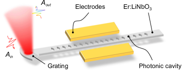
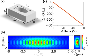
The setup that we consider is shown diagrammatically in Fig. 1. A photonic-crystal nano-beam cavity is fabricated in an Er3+:LiNbO3 thin film. Light is input into (and output from) a one-sided cavity through a grating coupler. Two electrodes are used to supply electric field to utilize the electro-optic effect of LiNbO3. The width and the thickness of the cavity are nm and nm, respectively. A photonic bandgap around 1.5 m is obtained by milling oval holes with nm, nm, and a period of nm, as illustrated in Fig. 2(a). A cavity resonance is formed by changing the period of the five central holes to nm. Figure 2(b) shows the simulated electric-field distribution of the cavity at the resonant wavelength of 1.5 m.
The effective refractive index of LiNbO3 in our simulations is modelled as , where is the refractive index of LiNbO3 without applied voltage, is a constant related to the electro-optic coefficient of LiNbO3 [34], and is the applied DC electric field. According to our simulations, the cavity frequency shifts linearly with the change of refractive-index: , as shown in Fig.2(c). Applying a 10 V voltage to the structure can shift the frequency by approximately 60 GHz.
For a collection of two-level erbium ions interacting with such an optical cavity, the dynamic equations for an ion are:
| (1) |
where are the elements of the two-level density matrix with , indicating the ground and excited state respectively, is the cavity-mode operator, is the atomic frequencies, is the excited-state lifetime, is the optical coherence time, and denotes the single-photon Rabi frequency. It is assumed in the above equations that the cavity and atomic operators are uncorrelated, which is a good approximation even in the regime of single excitation. The inhomogeneous atomic detuning is subject to a Gaussian distribution , where is the center of the inhomogeneous line, and . The ensemble polarization of erbium ions is
| (2) |
where is the total number of erbium ions.
Different from plane wave propagating along a crystal, when light is input into a cavity [35, 36], the time that the optical field needs to form a stable distribution inside the cavity is , where is the coupling loss of the cavity. This means that the optical field can form a stable cavity mode within a time scale (ns, as shown below) much less than the coherence time and the spontaneous lifetime (ms) of the erbium ions. Therefore, one can use the creation and annihilation operators to describe the dynamics of the cavity modes. The equation of motion for the cavity mode is
| (3) |
where is the input driving field ( signal pulse or control pulses in our case).
Since the cavity frequency can be electrically shifted, according to the Purcell effect [37], emission of the atomic ensemble can either be suppressed if is off-resonance with the atomic frequency, or enhanced if it is on-resonance. Note also that the DC-stark shift coefficient of erbium ions in LiNbO3 is typically 10 kHz/(Vcm-1) [38], which means that the ion frequency can also be shifted by 100 MHz under the investigated conditions. On one hand, such a shift of the erbium ions is negligible compared to the shift. On the other hand, applying another DC field with opposite polarity can easily cancel the effect of the erbium Stark shift on the memory. Moreover, because the Stark interaction of rare-earth-doped crystals tends to be anisotropic, it is possible to detune the ion frequency in the opposite direction to the cavity frequency, being an advantage due to the enhanced ion-cavity detuning.
Based on the effect of , we can both silence the first echo and enhance the second by applying a DC electric field. To get an intuitive picture of the requirements of our scheme, we first consider an input optical pulse with a linewidth much narrower than . In such a case the field inside the cavity can instantaneously follow the variation of the signal field, i.e., the adiabatic approximation applies. Note also that the input-output relation of a cavity is
| (4) |
At the echo-emission stage when the input is absent, one can write the output of the cavity as
| (5) |
The polarization term in Eq.(5) originates from the stored collective excitation of the erbium ions. It is clear now if can be detuned to a value much larger than , the output echo can be effectively silenced.
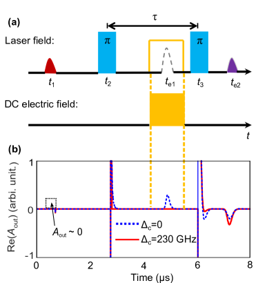
The sequences of control optical pulses and applied voltage of our scheme are illustrated in Fig. 3(a):
-
I.
At , an optical pulse, which is the signal to be stored, enters the cavity. To obtain high-efficiency quantum storage, perfect absorption of the input pulse is needed. For a weak input pulse with few photons (then applies), the polarization term is a linear function of the cavity field: , with being a constant. If (the cavity mode can instantaneously follow the change of input pulse), we can obtain from Eq. (3) and (4) that
(6) When , there is impedance-matching leading to ideal absorption of the input pulse [39, 40]. By designing the coupling loss of the input grating coupler and choosing a proper density of erbium ions , the impedance matching condition can be reached so that the input pulse are perfectly absorbed, resulting in .
-
II.
At , a rephasing -pulse is applied to the erbium ensemble, which reverses the phase of .
-
III.
At , where , the coherence with respect to different detuning restores in phase and stimulates an echo. If no voltage is applied, the echo would be emitted into the LiNbO3 cavity. As aforementioned, this echo is noisy and not suitable for quantum memories. To silence this echo, an external electric field is applied between and , as shown by the DC field sequence in Fig. 3(a). The DC field can shift the cavity frequency out of resonance with the rephased collective polarization , suppressing the collective emission as an echo.
-
IV.
At , where , a second -pulse is applied to cancel the phase differences accumulated between and , and, in addition, to bring those ions excited by the first pulse back to their ground states.
-
V.
At , where , a secondary echo with low noise is released from the cavity.
To show that efficient storage is experimentally feasible, we calculate the output of the scheme by numerically solving Eq. (1)-(4). In the present work, the focus is on proposing the principles and mechanisms of a storage scheme, and the building and computation of the realistic model [41] will be addressed in future work . The loaded quality-factor of the nano-beam cavity is (the intrinsic in simulations can be as high as ), and the mode volume of which is . While erbium ions in bulk LiNbO3 crystal have an inhomogeneous linewidth of GHz and optical coherence time of ms and electric dipole moment of Cm [13], we used the parameters when erbium ions are doped in LiNbO3 thin film, which are G GHz and ms[42].
The performance with (red line) and without (blue dashed line) an applied voltage is shown in Fig. 3(b). At , a light pulse with a duration of 0.16 s is input to the cavity. According to a given coupling loss of our cavity, we set the concentration of erbium ion as 225 ppm to realize the impedance-matching condition. Perfect absorption is observed in Fig. 3(b), where the output at is .
With the absence of an applied DC field, both a primary echo and a secondary echo can be seen after applying pulses, as shown by the blue dashed line in Fig. 3(b). However, if an electrical field is turned on to shift 230 GHz out of resonance during the emission period of the first echo, the first echo can be silenced to a negligible level. At the same time the amplitude of the second echo, compared to its counterpart without applied field, is enhanced. These results suggest that one can both silence the unwanted echo and enhance the second by using the electro-optic effect of LiNbO3.
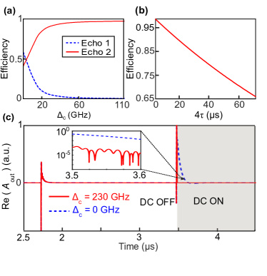
To efficiently cancel the first echo, one needs a large as suggested by Eq (5). In Fig. 4(a), we compare the emissions of the two echoes for increasing . When there is no external DC field , both the first and the second echo are present and of similar weights. With increasing , the efficiency of the second echo rises up to 97%, accompanied by the decrease of the first one. Note that to obtain a high-contrast ratio between the first and the second echo, is just required to be larger than the cavity linewidth (2 GHz in our case), rather than the inhomogeneous linewidth of erbium ions (166 GHz in our case). This is evident in Fig. 4(a), where for GHz the ratio between the first and the second echo is already 1.3%. Therefore a high-Q cavity can reduce the needed DC voltage and facilitate the application of the scheme.
Further increasing above 60 GHz leads to little increase of the efficiency above . This is because the memory operation takes time, during which some ions decohere and cannot be rephased by -pulses. The efficiency depends on the decoherence time according to , where is twice the interval between the signal pulse and the revival echo, as shown in Fig. 4(b). In this paper, s is used from a relevant experiment that measured the coherence time of erbium ions in thin-film LiNbO3 waveguides [43]. When rare-earth ions are doped into LiNbO3, static defects like charge compensation and compositional disorder cause large inhomogeneous linewidths and can also lead to decoherence [44]. In addition, the presence of non-zero nuclear spin isotopes 93Nb, 7Li, and 6Li causes additional decoherence due to their dynamic magnetic interactions with erbium ions. Note that the s in our scheme already enables a theoretical efficiency of 97%. If the operation time is reduced, such an efficiency can be extended to meet the requirement of quantum-error-correction applications [45]. To further extend the memory storage time without losing high efficiency, one can use the hyperfine ground states of erbium ions. When an erbium isotope with nonzero nuclear spin is used, hyperfine ground states offer the possibility of realizing the Zero-First-Order-Zeeman effect, showing the prospects of extending the coherence times by orders of magnitudes [53, 54, 55].
By introducing a tunable LiNbO3 cavity, not only can the emission of echoes be controlled, but also the noise of such a memory can be suppressed to a negligible level, as shown in Fig. 4(c). For quantum memories based on photon echoes, typical noise originates from free induction decay or spontaneous emission generated by -pulses. Shown in Fig. 4(c) is the output with pulses present but no input signal. Without an applied electric field, the free-induction-decay tails of both pulses immediately arise once the pulses are switched off, as shown by the blue dashed curve of Fig. 4(c). If an electric field is applied after the second pulse to shift the cavity frequency by 230 GHz, both the free induction decay and spontaneous emission (red curve) are suppressed. In our calculations, a ratio of more than 104 between the noise levels with and without an applied field can be obtained, as shown in the inset of Fig. 4(c). The low noise thus makes the memory suitable for working at single photon levels. If the input optical state is a one-photon state, then the noise-limited fidelity of the output, according to the calculation method in reference [46], can be more than 99.8% (depending on the read-out time of the memory).
In our scheme, the primary echo is silenced by . This is quite different from other protocols such as the Revival-of–Silenced-Echo (ROSE) scheme that utilizes the spacial phase mismatching effect[47], the Hybrid-Photon-Echo-Rephasing scheme that utilizes the electric Stark effect[48], and the Light-Shift-Photon-Echo-Rephasing scheme that utilizes the light-induced frequency shift effect[49]. The echo cancellation in all these schemes is the result of a vanishing ensemble polarization due to the destructive interference of ions with different accumulated phases (spatial or temporal). At the moment of our scheme, all ions are already rephased, which means that an ensemble polarization is built up and can otherwise emit photons if is in tune. The silenced echo is based on the Purcell effect rather than the out-of-phase superposition of ions. This difference has brought several advantages, as listed below, to our scheme.
The most important one is that the scheme not only shifts the requirement on controllability from erbium ions to LiNbO3, but also bring in the feature of LiNbO3. Many memory protocols, such as CRIB and AFC, rely on preparation steps. The preparation not only introduces technical difficulties, but also imposes additional requirements on working ions. For example, in addition to excellent coherence properties of working ions, CRIB also relies on extra electric or magentic field to realize controllable linewidth broadening, which can lead to a compromise between coherence and controllability. The AFC protocol only works for ions with auxiliary long-life-time states. In our scheme, all these requirements are relaxed. When building a memory, one can just focus on utilizing the best experimental conditions to achieve the longest coherence time, as the write-in and read-out of the memory are now controlled by the LiNbO3. This means that the protocol can take full advantage of the 1.5 m telecom emission and the long coherence times of erbium ions. Moreover, benefiting from the host LiNbO3 thin film, such a device is easy to integrate within modern photonic circuits. The number of memory units can be scaled up with current technology, and the operation of each unit can be independently controlled by electrodes, ideal for integrated quantum chips.
| Q | V() | Efficiency() | ||
|---|---|---|---|---|
| 0.28 | 105 | 3.1 | 97 | |
| 0.3 | 70 | 2.2 | 97 | |
| 0.28 | 50 | 1.5 | 97 | |
| 0.26 | 26 | 0.7 | 97 | |
| 0.23 | 3 | 0.07 | 97 |
The multimode capacity of the memory can be limited by the linewidth of the optical cavity. In the above calculation, the linewidth of the cavity is GHz and the input pulse is MHz, thus the multimode capacity is on the order of . Using a high cavity reduces the multimode capacity, but on the other hand, can further enhance the light-matter interaction. For high cavities, fewer erbium ions are needed for high optical absorption, which, together with the small mode volume of photonic-crystal cavities, enables us to exploit the possibility of quantum memories based on single ions. The numerical results of calculations on for several combinations of and erbium concentrations are shown in Table 1 (note that in these calculations, the mode volume V and the duration of the two pulses are also adjusted to maintain the efficiency ). The number of ions that can be resolved in its homogeneous linewidth is approximated by , where 1 MHz is chosen for the homogeneous linewidth , and GHz is the inhomogeneous linewidth [42]. For (LiNbO3 micro cavities with has been reported [50]), the number of interacting erbium ions can easily be reduced to single digits. For erbium doped crystals with Gaussian broadening, working on the edge of the inhomogeneous line can further reduce and facilitate single ion detection. With decreasing erbium concentration, the scheme shows potential for realizing solid-state single-ion quantum memories, where the property of addressable single ions can be used to predict events of successful storage [51] and to establish deterministic entanglement [52].
In summary, we propose an on-chip quantum memory scheme by utilizing the electric-optic effect of LiNbO3. Applying a DC electric field can change the refractive index of LiNbO3 and the frequency. Therefore, it can change the frequency of a LiNbO3 photonic cavity and control the emission of echoes due to the Purcell effect. Our numerical results show that the echo readout efficiency approaches unity. Compared with the technical difficulties in memory schemes, the electric-field controllability of lithium niobate on a phtonic chip is industrially compatible. It has been demonstrated that the erbium ions in a patterned thin-film LiNbO3 are able to preserve the coherence properties of bulk material. At high magnetic field and low concentrations, the coherence time can be further extended, which in turn can increase the maximum memory efficiency. Furthermore, when an erbium isotope with nonzero nuclear spin is used, hyperfine interactions offer the possibility of using the ZEFOZ effect[53, 54, 55] to extend the coherence times by orders of magnitude. We thus expect it is experimentally feasible to build an integrated quantum memory with high efficiency and long coherence times using Er3+:LiNbO3 thin films. The scheme also offers new ideas for exploiting quantum memories, such as noise suppression by electric fields and single-ion quantum memories.
The authors wish to acknowledge financial support from the National Natural Science Foundation of China (No. 62105033 and No. 12174026), the Start-up Fund of Beijing Institute of Technology, and the Science and Technology Innovation Project of Beijing Institute of Technology.
References
- [1] S. Wehner, D. Elkouss, and R. Hanson, Quantum internet: a vision for the road ahead, Science, 362, eaam9288 (2018).
- [2] C. Simon, Towards a global quantum network, Nat. Photonics, 11, 678 (2017).
- [3] S. F. Bush, W. A. Challener, and G. Mantelet, A perspective on industrial quantum networks, AVS Quantum Sci, 3, 030501 (2021).
- [4] R. Van Meter and S. J. Devitt, The path to scalable distributed quantum Computing, Computer, 49, 31 (2016).
- [5] Z. Eldredge, M. Foss-Feig, J. A, Gross, S. L. Rolston, and A. V. Gorshkov, Optimal and secure measurement protocols for quantum sensor networks, Phys. Rev. A, 97, 042337 (2018).
- [6] T. Zhong and P. Goldner, Emerging rare-earth doped material platforms for quantum nanophotonics, Nanophotonics, 8, 2003 (2019).
- [7] A. I. Lvovsky, B. C. Sanders, and W. Tittel, Optical quantum memory, Nat. Photonics, 3, 706 (2009).
- [8] F. Arute, et al., Quantum supremacy using a programmable superconducting processor, Nature, 574, 505 (2019).
- [9] A. Reiserer, Colloquium:Cavity-enhanced quantum network nodes, Rev. Mod. Phys., 94, 041003 (2022)
- [10] C. Liu, T.-X. Zhu, M.-X. Su, Y.-Z. Ma, and G.-C. Guo, On-demand quantum storage of photonic qubits in an on-chip waveguide, Phys. Rev. Lett., 125, 260504 (2020).
- [11] I. Craiciu, M. Lei, J. Rochman, J. G. Bartholomew, and A. Faraon, Multifunctional on-chip storage at telecommunication wavelength for quantum networks, Optica, 8, 114 (2020).
- [12] T. Zhong , J. M. Kindem , J. G. Bartholomew , J. Rochman , I. Craiciu , E. Miyazono , M. Bettinelli , E. Cavalli , V. Verma , S. W. Nam , F. Marsili , M. D. Shaw , A. D. Beyer , and A. Faraon, Nanophotonic rare-earth quantum memory with optically controlled retrieval,Science , 357, 1392 (2017).
- [13] C. Thiel, T. Böttger, and R. Cone, Rare-earth-doped materials for applications in quantum information storage and signal processing, J. Lumin., 131, 353 (2011).
- [14] T. Zhong, J. M. Kindem, J. G. Bartholomew, J. Rochman, I. Craiciu, E. Miyazono, M. Bettinelli, E. Cavalli, V. Verma, S. W. Nam, F. Marsili, M. D. Shaw, A. D. Beyer, and A. Faraon, Nanophotonic rare-earth quantum memory with optically controlled retrieval, Science, 1395, 1392 (2017).
- [15] T. Zhong, J. M. Kindeml, E. Miyazono1, and A. Faraonl, Nanophotonic coherent light–matter interfaces based on rare-earth-doped crystals, Nat. Commun., 6, 8206 (2015).
- [16] C. Liu, Z.-Q. Zhou, T.-X. Zhu, L. Zheng, M. Jin, X. Liu, P.-Y. Li, J. Y. Huang, Y. Ma, T. Tu, T.-S. Yang, C.-F. Li, and G.-C. Guo, Reliable coherent optical memory based on a laser-written waveguide, Optica, 7, 192 (2020).
- [17] E. Saglamyurek, N. Sinclair, J. Jin, J. A. Slater, D. Oblak, W. Tittel, F. Bussières, M. George, R. Ricken, and W. Sohler, Broadband waveguide quantum memory for entangled photons, Nature, 469, 512 (2010).
- [18] C. Liu, T.-X. Zhu, M.-X. Su, Y.-Z. Ma, Z.-Q. Zhou, C.-F. Li, and G.-C. Guo, On-demand quantum storage of photonic qubits in an on-chip waveguide, Phys. Rev. Lett., 125, 260504 (2020).
- [19] Y.-H. Chen, S. P. Horvath, J. J. Longdell, and X.-D. Zhang, Optically Unstable Phase from Ion-Ion Interactions in an Erbium-Doped Crystal, Phys. Rev. Lett., 126, 110601 (2021).
- [20] J. J. Longdell and M. J. Sellars, Analytic treatment of controlled reversible inhomogeneous broadening quantum memories for light using two-level atoms, Phys. Rev. A, 78, 032337 (2008).
- [21] D. B. Higginbottom, B. M. Sparkes, M. Rancic, O. Pinel, M. Hosseini, P. K. Lam, and B. C. Buchler, Spatial mode storage in a gradient echo memory, Phys. Rev. A, 86, 023801 (2012).
- [22] Y.-W. Cho, G. T. Campbell, J. L. Everett, J. Bernu, D. B. Higginbottom, M. T. Cao, J. Geng, N. P. Robins, P. K. Lam, and B. C. Buchler, Highly efficient optical quantum memory with long coherence time in cold atoms, Optica, 3, 100 (2016).
- [23] J. Dajczgewand, J. L. Le Gouët, A. Louchet-Chauvet, and T. Chanelière, Large efficiency at telecom wavelength for optical quantum memories, Opt. Lett., 39, 2711 (2014).
- [24] S. Wang, L. Yang, R. Cheng, Y. Xu, M. Shen, R. L. Cone, C. W. Thiel, and H. X. Tang, Incorporation of erbium ions into thin-film lithium niobate integrated photonics, Appl. Phys. Lett., 116, 151103 (2020).
- [25] M. Wang, Y. Xu, Z. Fang, Y. Liao, P. Wang, W. Chu, L. Qiao, J. Lin, W. Fang, and Y. Cheng, On-chip electro-optic tuning of a lithium niobate microresonator with integrated in-plane microelectrodes, Opt. Express, 25, 124 (2017).
- [26] M. Li, J. Ling, Y. He, U. A. Javid, and Q. Lin, Lithium niobate photonic-crystal electro-optic modulator, Nat. Commun., 11, 4123 (2020).
- [27] Q. Luo, C. Yang, R. Zhang, Z. Z. Hao, D. H. Zheng, H. D. Liu, X. Y. Yu, F. Gao, F. Bo, Y. Kong, G. Q. Zhang, and J. Xu, On-chip erbium-doped lithium niobate microring lasers, Opt. Lett., 46, 3275 (2021).
- [28] M. Afzelius, N. Sangouard, G. Johansson, M. U. Staudt, and C. M. Wilson, Proposal for a coherent quantum memory for propagating microwave photons, New J. Phys., 15, 065008 (2013).
- [29] B. Julsgaard, C. Grezes, P. Bertet, and K. Mølmer, Quantum memory for microwave photons in an inhomogeneously broadened spin ensemble, Phys. Rev. Lett., 110, 250503 (2013).
- [30] V. Ranjan, Y. Wen, A.K.V. Keyser, S. E. Kubatkin, A. V. Danilov, T. Lindstrm, P. Bertet, and S. E. de Graaf, Spin-Echo Silencing Using a Current-Biased Frequency-Tunable Resonator, Phys. Rev. Lett., 129, 180504 (2022).
- [31] S. A. Moiseev and B. S. Ham, Photon-echo quantum memory with efficient multipulse readings, Phys. Rev. A, 70, 063809 (2004).
- [32] Y.-Z. Ma, M. Jin, D.-L. Chen, Z.-Q. Zhou, C.-F. Li, and G.-C. Guo, Elimination of noise in optically rephased photon echoes, Nat. Commun., 12, 4378 (2021).
- [33] J. Ruggiero, J. Gouët, C. Simon, and T. Chanelière, Why the two-pulse photon echo is not a good quantum memory protocol, Phys. Rev. A, 79, 053851 (2009).
- [34] A. Pan, C. R. Hu, C. Zeng, and J. S. Xia, Fundamental mode hybridization in a thin film lithium niobate ridge waveguide, Opt. Express, 27, 35659 (2019).
- [35] J. J. Longdell, G. Hétet, P. K. Lam, and M. J. Sellars, Analytic treatment of controlled reversible inhomogeneous broadening quantum memories for light using two-level atoms, Phys. Rev. A , 78, 032337 (2008).
- [36] P. M. Ledingham, W. R. Naylor, J. J. Longdell, S. E. Beavan, and M. J. Sellars, Nonclassical photon streams using rephased amplified spontaneous emission, Phys. Rev. A ,81, 012301 (2010)
- [37] E. M. Purcell, Spontaneous emission probabilities at radio frequencies, Phys. Rev., 69, 674 (1946).
- [38] S. R. Hastings-Simon, M. U. Staudt, M. Afzelius, P. Baldi, D. Jaccard, W. Tittel, and N. Gisin, Controlled Stark shifts in Er3+-doped crystalline and amorphous waveguides for quantum state storage, Opt. Commun., 266, 716 (2006).
- [39] S. A. Moiseev, S. N. Andrianov, and F. F. Gubaidullin, Efficient multimode quantum memory based on photon echo in an optimal QED cavity, Phys. Rev. A, 82, 022311 (2010).
- [40] M. Afzelius and C. Simon, Impedance-matched cavity quantum memory, Phys. Rev. A, 82, 022310 (2010).
- [41] J.S. Kollath-Bönig,Cavity-based quantum memory for light with inhomogeneously coupled atoms,Master’s thesis, (2018)
- [42] C. W. Thiel, R. M. Macfarlane, T. Böttger, Y. Sun, R. L. Cone, and W. R.Babbitt, Optical decoherence and persistent spectral hole burning in Er3+:LiNbO3 , J. Lumin., 130, 1603 (2010).
- [43] S. Wang, L. Yang, M. Shen, W. Fu, Y. Xu, R. L. Cone, C. W. Thiel, and H. X. Tang, Er:LiNbO3 with High Optical Coherence Enabling Optical Thickness Control, Phys. Rev. Appl., 18, 014069 (2022).
- [44] R. M. Macfarlane, Y. Sun, R. L. Cone, C. W. Thiel and R. W. Equall, Optical dephasing by disorder modes in yttrium orthosilicate (Y2SiO5 ) doped with Eu3+, J. Lumin., 107, 310 (2004).
- [45] J. M. Chow, J. M. Gambetta, A. D. Córcoles, S. T. Merkel, J. A. Smolin, C. Rigetti, S. Poletto, G. A. Keefe, M. B. Rothwell, J. R. Rozen, M. B. Ketchen, and M. Steffen, Universal Quantum Gate Set Approaching Fault-Tolerant Thresholds with Superconducting Qubits, Phys. Rev. Lett., 109, 060501 (2012).
- [46] P. Jobez, C. Laplane, N. Timoney, N. Gisin, A. Ferrier, P. Goldner, and M. Afzelius, Solid State Spin-Wave Quantum Memory for Time-Bin Qubits, Phys. Rev. Lett., 114, 230501 (2015).
- [47] V. Damon, M. Bonarota, A. Louchet-Chauvet, T. Chanelière, and J. Gouët, Revival of silenced echo and quantum memory for light, New J. Phys., 13, 093031 (2011).
- [48] D. L. Mcauslan, P. M. Ledingham, W. R. Naylor, S. E. Beavan, and J. J. Longdell, Photon-echo quantum memories in inhomogeneously broadened two-level atoms, Phys. Rev. A, 84, 022309 (2011).
- [49] H. C. McDonald, Controlling photon echoes with the light shift, Master’s thesis (2016).
- [50] T. J. Wang, G. L. Peng, M. Chan, and C. H. Chen, On-chip optical microresonators with high electro-optic tuning efficiency, J. Lightwave Technol., 38, 1851 (2020).
- [51] H. P. Specht, C. Nölleke, A. Reiserer, M. Uphoff, E. Figueroa, S. Ritter, and G. Rempe, A single-atom quantum memory, Nature, 473, 190 (2011).
- [52] J. I. Cirac, P. Zoller, H. J. Kimble, and H. Mabuchi, Quantum state transfer and entanglement distribution among distant nodes in a quantum network, Phys. Rev. Lett., 78, 3221 (1996).
- [53] M. Rančić, M. P. Hedges, R. L. Ahlefeldt, and M. J. Sellars, Coherence time of over a second in a telecom-compatible quantum memory storage material, Nat. Phys., 14, 50 (2018).
- [54] Y.-H. Chen, X. Fernandez-Gonzalvo, and J. J. Longdell, Coupling erbium spins to a three-dimensional superconducting cavity at zero magnetic field, Phys. Rev. B, 94, 075117 (2016).
- [55] J. V. Rakonjac, Y.-H. Chen, S. P. Horvath, and J. J. Longdell, Long spin coherence times in the ground state and in an optically excited state of 167Er3+: Y2SiO5 at zero magnetic field, Phys. Rev. B, 101, 184430 (2020).