Strong light-matter interactions between gap plasmons and two-dimensional excitons at ambient condition in a deterministic way
Abstract
Strong exciton-plasmon interaction between the layered two-dimensional (2D) semiconductors and gap plasmons shows a great potential to implement cavity quantum-electrodynamics in ambient condition. However, achieving a robust plasmon-exciton coupling with nanocavity is still very challenging, because the layer area is usually small with conventional approaches. Here, we report on a robust strong exciton-plasmon coupling between the gap mode of bowtie and the excitons in MoS2 layers with gold-assisted mechanical exfoliation and the nondestructive wet transfer techniques for large-area layer. Benefiting from the ultrasmall mode volume and strong in-plane field, the estimated effective exciton number contributing to the coupling is largely reduced. With a corrected exciton transition dipole moment, the exciton numbers are extracted with 40 for the case of monolayer and 48 for 8 layers. Our work paves a way to realize the strong coupling with 2D materials with few excitons at room temperature.
I Introduction
Atomically thin transition metal dichalcogenides (TMDs) have been exploited widely for numerous optoelectronics and photonics applications, including single-photon emitters Chakraborty et al. (2015); Dang et al. (2020), transistors Zhang et al. (2012); Radisavljevic et al. (2011), photodetectors Mak et al. (2014); Lopez-Sanchez et al. (2013) and valleytronic devices Xiao et al. (2012); Cao et al. (2012). One of the intriguing properties is the large exciton binding energy Ugeda et al. (2014); He et al. (2014), providing the opportunity to study the interaction of light and matter at room temperature when they are embedded in a microcavity Lundt et al. (2016); Wang et al. (2016). When the rate of coherent energy transfer between excitonic transition and photons in cavity is faster than their average dissipation rate, the system goes into strong coupling regime, resulting in the formation of part-light and part-matter bosonic quasiparticles called microcavity polaritons Liu et al. (2015); Törmä and Barnes (2015). Polaritons in microcavities provide excellent platforms to realize Bose-Einstein condensation Deng et al. (2002); Kasprzak et al. (2006), low-threshold lasing Christopoulos et al. (2007); Kéna-Cohen and Forrest (2010), low-energy switching Dreismann et al. (2016); Ballarini et al. (2013) and quantum information processing Wallraff et al. (2004); Amo et al. (2010).
In order to achieve strong coupling with excitons in TMDs, optical cavities such as FabryProt cavities and photonic crystal microcavities Xie et al. (2020); Qian et al. (2019) have been employed widely at cryogenic temperatures and in high vacuum Dufferwiel et al. (2015); Chen et al. (2017). Even though a few of them have been used to demonstrate strong coupling at room temperature Liu et al. (2015); Zhang et al. (2018); Flatten et al. (2016), the Rabi splittings are on the order of thermal energy ( meV) Kleemann et al. (2017); Hu and Fei (2020). Plasmonic nanocavities such as individual metallic nanoparticles Chikkaraddy et al. (2016) or dimers Santhosh et al. (2016) can provide surface plasmon polaritons (SPPs) with light confined at subwavelength scale, which is an alternative choice for realizing strong coupling at ambient conditions, for example, coupled system with nanoparticle and layered TMDs Kleemann et al. (2017); Zheng et al. (2017); Stührenberg et al. (2018); Qin et al. (2020); Han et al. (2018).
The plasmonic nanocavities with mode volumes beyond the diffraction limit make it possible to demonstrate strong coupling with a small number of excitons, which has rich applications in the research of quantum many-body phenomenaHartmann et al. (2008), photon blockade with many emittersTrivedi et al. (2019), cavity cooling Hosseini et al. (2017) and so on. Recently, the gap plasmon systems with ultimate field confinement have been used to realize strong coupling with single molecules Chikkaraddy et al. (2016) and single quantum dots Santhosh et al. (2016), indicating a potential for applications at the quantum optics level Hennessy et al. (2007); Faraon et al. (2008). For layered TMDs, particle-on-film systems with nanoparticles Qi et al. (2020), or single plasmonic structures such as nanorods Wen et al. (2017), nanodisks Geisler et al. (2019) or nanocuboid Lo et al. (2019) have been used to demonstrate strong coupling. However, drop-casted nanoparitcles induce the randomness intrinsically, which cannot guarantee the robustness and the reproducibility in a deterministic way. The robustness is very important for the strong coupled system with a small number of excitons in particular Liu et al. (2017); Tame et al. (2013). In addition, the resonant optical field in such cavities is typically polarised perpendicularly to the layer planes when embedded with two-dimensional semiconductors Kleemann et al. (2017); Qin et al. (2020), which impedes the efficient coupling with the exciton dipole oriented almost in-plane. Therefore, engineering orientations of exciton dipole and cavity modes precisely is highly desired to large coupling strength with a small number of excitons.
To demonstrate the strong coupling in plasmon-exciton (”plexciton”) with few excitons, the exciton number estimation is crucial. So far, the exciton number extraction with different ways shows a very large discrepancy Wen et al. (2017); Qin et al. (2020); Han et al. (2018); Wang et al. (2019); Zheng et al. (2017); Liu et al. (2021). Experimentally, the exciton number evolved in the strongly coupled system is related to the coupling strength, mode volume and the exciton transition dipole moment of TMDs Qin et al. (2020). The coupling strength can be measured and the mode volume can be calculated with a good accuracy. It is noticed that the exciton transition dipole moment brings the main difference in previous work, which has been calculated with traditional quantum well recombination model Asada et al. (1984) or extracted with absorption spectra Zheng et al. (2017). Here, we verify the two methods and correct the transition dipole moment values for the exciton number estimation.
In this work, we report on an observation of robust strong plasmon-exciton coupling between gap plasmons confined within individual gold bowties and excitons in MoS2 layers at ambient conditions utilizing the gold-assisted mechanical exfoliation method and wet transfer techniques. Due to the strong in-plane electric field inside the material and small mode volume introduced by the bowtie resonator, vacuum Rabi splittings up to 110 meV and 80 meV are obtained for the coupling systems with 8-layer and monolayer MoS2, respectively. The estimated effective exciton number contributing to the coupling with gap mode is reduced to for the case of monolayer and for the case of 8 layers with a corrected dipole moment. The robust strong plasmon-exciton coupling with less exciton number paves a way for future scalable integrated nanophotonic devices.
II Results and discussion
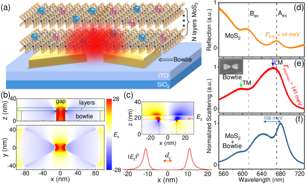
Figure 1a shows a schematic diagram of the plasmon-exciton coupling system with layered MoS2 on top of a bowtie nanostructure. Here, the gold bowtie is employed as a plasmonic nancavity for two reasons. First, it provides an ultra-confined gap plasmon mode with a mode volume of around Santhosh et al. (2016); Lee et al. (2015). More importantly, when the high-refractive-index MoS2 layers is covered to the surface of bowtie, the strongly confined in-plane electric component of gap mode is expanding in the material (as shown Fig. 1b) calculated with the finite-difference time-domain method, indicating the excitons above the gap will be strongly coupled to the gap mode. Normally in particle-on-film systems, the main electric field of the gap plasmon is dominated by out-of-plane component () Kleemann et al. (2017); Qin et al. (2020) and strong coupling is achieved with the contribution of a large number of excitons. Our configuration is more suitable to enhance the coupling strength for the monolayer TMDs with completely in-plane dipole orientation or few layers with in-plane dipole strength dominated Schuller et al. (2013).
To further compress the exciton number contributing to plasmon-exciton interaction, a localized electric field region comparable to the effective exciton area is required. The excitons in TMDs are delocalized quasiparticles formed in semiconductor band gaps and extending much larger than single unit cell Baranov et al. (2018) with the exciton coherence length is nm for monolayer MoS2 (Sec. III of the Supporting Information (SI)). Figure 1c shows the distribution of out-of-plane component of the gap mode. It can be seen that the electric fields between two tips have opposite phases, but the intensities rapidly decay to zero inside the gap. Therefore, a gap distance slightly larger than the exciton coherence length should be able to couple the gap mode to few excitons with a constructive interference. In our device, the bowtie nanocavity was designed with a gap distance of about 20 nm. The corresponding dark-field (DF) scattering spectrum (Fig. 1e) shows a well-defined longitudinal gap mode at about 1.87 eV and a transverse mode at about 2.07 eV (Fig. S7 in the SI). Clearly, the longitudinal gap mode overlaps with the emission peak of A exciton of MoS2 (Fig. 1d), satisfying the requirement of spectral coincidence.
Furthermore, a stable and reproducible coupled system is important to achieve strong coupling especially at few-exciton level, which has been an issue for systems based on colloidal quantum dots, molecules and TMDs Chikkaraddy et al. (2016); Santhosh et al. (2016); Hartsfield et al. (2015); Yan and Wei (2020) because of the randomness in exciton materials or plasmon nanocavities Baranov et al. (2018). Here, we have made two efforts to address this problem. First, a contamination-free, one-step and universal gold-assisted mechanical exfoliation method Huang et al. (2020) has been used to obtain millimeter-size mono-/multilayer MoS2 (Sec. I of the SI for more details), based on the covalent-like quasi bonding between Au adhesion layer and layered crystal. The quality of obtained MoS2 layers is similar to that of the flakes prepared by traditional mechanical exfoliation, with clear Raman signals and photoluminescence from excitons (Fig. S4 and Fig. S5 in the SI). This exfoliation method with high yield ratio and large-area layers is essential for the rest systematic studies. Second, to guarantee the stability of the coupled systems, a nondestructive wetting transfer method has been used to transfer thin layers to the prepared nanocavities, without damaging the fragile nanostructures during the transfer process (see Sec. I of the SI for more details). As a result, a splitting of about 106 meV is achieved in a coupled system with resonators combined with 8-layer MoS2 (as shown in Fig. 1f).
To verify the coupled system is in strong coupling regime, tuning the plasmon mode to cross the energy of A exciton is required. In most cases, the tuning comes from randomly distributed nanoparticles with different sizes Chikkaraddy et al. (2016); Qin et al. (2020); Stührenberg et al. (2018); Han et al. (2018). Since the energy of plasmon is sensitive to the particle size, this inevitably limits the reliability and repeatability of the system. Particularly for MoS2, the splitting of spin-orbit coupling is close to the value of Rabi splitting, complicating the study of such system because of the emission of B exciton. Here, increasing the gap distances of bowtie resonators has been used to tune gap modes in a more moderate way than tuning sizes (Fig. S10 and Fig. S11 in the SI).
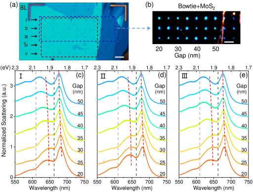
Figure 2a shows a bright-field image of the bowties covered with large area of MoS2 layers. It can be seen that the whole area is flat without any wrinkles due to the above exfoliation and transfer techniques. The smallest gap distances of bowties are nm and increase by approximate 5 nm for each step from left to right (Fig. S1 and Fig. S2 in the SI). The red dashed box indicates that there are five rows of bowties covered well by flakes, labelled with Roman numerals from one to five. Figure 2b shows the dark-field image of the first three rows. The clear and bright spots of hybrid nanostructures indicate the TMDs layers are combined well with the plasmonic resonators without extra wrinkles and bubbles.
The normalized scattering spectra from rows I, II, III (Fig. 2c, d, e) and IV, V (Fig. S15 in the SI) all show similar behaviors, indicating a good robustness. When the gap distance is around 20 nm, an obvious double-peaked splitting around the position of A exciton is observed, representing the energy of the upper plexciton branches (UPB) and lower plexciton branches (LPB). It is worth noting that the transferred MoS2 layers will change the dielectric environment of resonators and result in a slight redshift of plasmon mode due to the dielectric screening effect Zheng et al. (2017); Xu et al. (2003). With the increase of gap distance, the longitudinal mode continuously blueshifts and eventually crosses the excitonic transition (see Sec. II of the SI for the discussion of energy tuning between exciton and plasmon). To extract the peak energies of UPB and LPB with Lorentzian fitting method, we fix the resonance of B exciton at about the 2.0 eV according to the reflection spectrum in Figure 1d (see Fig. S17 in the SI for fitting details). The red dashed curves in the scattering spectra trace the dispersion of plexciton branches, showing that UPB is getting closer to the resonance of B exciton as the gap increases but doesn’t overlap with it, which means the longitudinal plasmon mode only couples with A exciton of MoS2 unambiguously here.
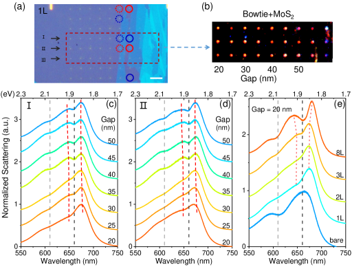
The similar splitting properties are also observed in the devices covered with monolayer. Figure 3a shows a bright-field image of the bowtie resonators with a large area of monolayer flake. The corresponding dark-field image is shown in Fig. 3b, where the resonator parameters are the same as those above. Figure 3c and d show the measured scattering spectra of line I and II with consistent spectral features (see Fig. S16 in the SI for line III). It can be seen that a relatively small splitting is observed compared with that of 8 layers. The splitting depending on layer thickness is also studied. As shown in Fig. 3e, the magnitude of splitting in spectra increases with the layer thickness with a gap distance at 20 nm, implying an increase of coupling strength with the number of layers. Although the strong coupling for all different layers has not been experimentally achieved, the splitting difference for different layer is obvious.
The coupled system can be described by the simplified Jaynes-Cummings model (JC model) given by Törmä and Barnes (2015); Qin et al. (2020); Qian et al. (2018):
| (1) |
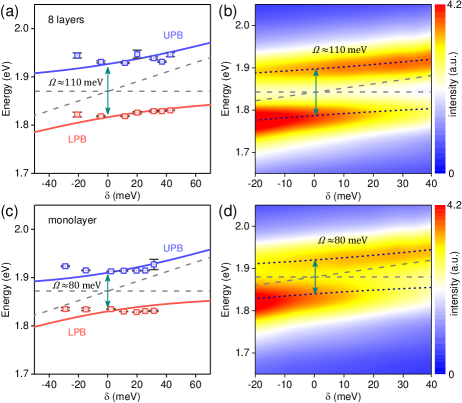
where , are the energies of plasmon and exciton respectively, is the detuning, and represents the coupling strength. A fit to the UPB and LPB peak energies using JC model is shown in Fig. 4a and c. As we can see, the errors of peak energies between different group of spectra are very small, showing the high robustness and reproducibility of the coupled system. The JC model fits to the peak energies show a Rabi splitting () about 110 meV for 8-layer devices, which satisfies the criteria for strong coupling (). While the Rabi splitting for the monolayer is approximately meV, indicating the system is in intermediate-coupling regime () Leng et al. (2018). Numerical calculations provide another piece of evidence for our observations. By modeling the excitonic dielectric permittivity of the MoS2 as a Lorentz oscillator, we calculated the scattering cross section of hybrid structures with changing the gap distance from 20 to 50 nm (Fig. 4b and d), showing an anticrossing of two normal modes.
Comparing with the calculated results, the intensity of UPB in experiment seems to be always lower than that of LPB, which can be due to the rapid attenuation of the gap mode with the increase of the gap and the non-negligible emission of uncoupled A exciton outside the nanocavity. The JC model fits and calculations also reveal the moderate anticrossing behavior of UPB and LPB in Fig. 4a and c. Due to the small tuning range of plasmon mode with increasing gap sizes and the strong coupling of exciton and plasmon optimized to near resonance, the energies of UPB and LPB move more slowly compared with that of plasmon mode during tuning process, making the data points looks horizontal and less curved. Additionally, the small number of excitons contributing to the coupling with gap mode also accounts for the mismatch between JC model fits and plexciton branches because of the strong background signal. For example, the emission of massive uncoupled excitons near bowtie in scattering spectra will affect the extraction of plexciton branches.
To evaluate the exciton number evolved in the strong couling, we use , where is the effective exciton number coherently contributing to the interaction with the cavity, is exciton transition dipole moment, is the vacuum field amplitude Zengin et al. (2015); Törmä and Barnes (2015) and is unit vector, satisfy . Because the exciton dipole strength in TMDs is highly anisotropic Liang (1973); Schuller et al. (2013) and has an out-of-plane component in multilayers, the coupling strength can be written as
| (2) |
where and represent the in-plane and out-of-plane dipole moments respectively, and with being parallel to the two-dimensional semiconductors plane and being perpendicular to the plane. Therefore, coupling strength can be expressed as a form of contribution from in-plane and out-of-plane dipole moments: . Here, we define the ratio of in-plane field as , which represents the ratio of an integral of in-plane field components to the total electric field and can be numerically calculated by:
| (3) |
where represents the volume of excitonic material. Similarly, we can get the ratio of out-of-plane field with . Finally, the coupling strength can be written as
| (4) |
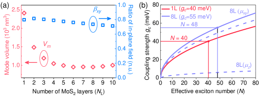
Figure 5a shows the mode volumes as a function of the layer number. The mode volume of bowtie nanocavity is about for monolayer, which is comparable to the current optimal results for a single nanoparticle such as gold bi-pyramids Stührenberg et al. (2018) or utrasmall gold nanorod Wen et al. (2017), and even smaller in the case with multiple layer covering. With layer number increasing, the mode volume gradually decreases from 2413 to 951 and then saturates. This means that the electric field is strengthened and more tightly confined in TMDs layers, which explains why larger splittings are observed in multilayers. The ratio of an integral of in-plane field to total field is about in different layers, as shown in Fig. 5a, confirming that the dominant electric field component of gap plasmon in our system is the in-plane component .
In order to estimate the number of excitons involved in coupling, transition dipole moment of the excitons in TMDs layer is another significant parameter. Here, we adopt two methods i.e. quantum well method and absorbance measurements to estimate this value. The quantum well method regards the 2D TMDs layer as quantum-well structures similar to III-V semiconductors Asada et al. (1984) and takes into account that the electron of TMDs has a large effective mass around the K point, giving , where is the transition energy of the exciton, is the band gap and is the spin-orbit splitting in the valence band. The absorbance measurements consider the relationship between the 2D susceptibility of excitons with 1 hydrogen-like wave function and absorption of the thin layer Zheng et al. (2017); Vasilevskiy et al. (2015), giving , where is the free space impedance, is the Bohr radius of exciton, and are the energy and linewith of exciton, respectively. Both methods give similar dipole moment values for TMDs layers, such as 7.53 Debye () and 5.63 for monolayer WS2 and 7.51 and 7.36 for monolayer MoS2, respectively (see Sec. III of the SI for more details). It should be noted that our calculation result is much smaller than the value of 56 reported in the literature Sie et al. (2015), where the reduced Plank constant () should have been used as discussed in the SI. For the case of several layers, we determined the in-plane dipole moment using , where is spectrally integrated for the A excitonic transition Wang et al. (2019). Using the value of monolayer, we obtain the in-plane dipole moment 5.07 and out of plane 1.01 .
| Structure | Materials | (meV) | N (*) | N (*) | N (*) |
|---|---|---|---|---|---|
| Single gold nanoprism on gold film (gap plasmon)Qin et al. (2020) | WS2 | 76 |
2
(56 ) |
111
(7.53 ) |
198
(5.63 ) |
| Single gold dimer (gap plasmon)Liu et al. (2021) | WS2 | 115.2-128.6 |
4.67-7.69
(56 ) |
258-425
(7.53 ) |
462-761
(5.63 ) |
| Single silver nanocube on silver film (gap plasmon) Han et al. (2018) | WS2 | 145 |
130
(56 ) |
7190
(7.53 ) |
12862
(5.63 ) |
| Silver nanoparticle array Wang et al. (2019) | WS2 | 52 |
3000
(50 ) |
132000
(7.53 ) |
236000
(5.63 ) |
| Single silver nanorod Zheng et al. (2017) | WSe2 | 49.5 |
4100
(7.67 ) |
||
| Single gold nanorod Wen et al. (2017) | WS2 | 106 | 12 |
225
(7.53 ) |
403
(5.63 ) |
| Our work: Single gold bowtie (gap plasmon) | MoS2 | 80-110 |
38
(7.51 ) |
40
(7.36 ) 48 (8 layer) |
* is the transition dipole moment in refs, is corrected transition dipole moment with quantum well model and is calculated with absorption spectra.
Fig. 5b shows the calculated coupling strength as a function of the effective exciton number for monolayer and 8 layers at resonance. We found the effective exciton number is compressed down to for the case of monolayer and in multilayers, indicating a small exciton number in such coupling system with plasmon modes and excitons in two-dimensional semiconductors. Table 1 shows the comparison of the coupled systems with small exciton number with some previous reports, in which the exciton numbers with corrected dipole moments are also included (see Sec. III of the SI for more details). The effective exciton numbers are much larger with corrected dipole moment than those as reported Qin et al. (2020); Han et al. (2018); Wang et al. (2019); Liu et al. (2021). The numbers involved in single nanorod structureWen et al. (2017) are recalculated by the formula at zero tuning. The calculated exciton numbers are also much larger than that as claimed. The small number of exciton in our experiment also explains the mismatch between JC model fitting and experimental results in Fig. 4a and c due to the influence of emission of massive uncoupled excitons in layers around the bowtie. For multilayers, the contribution to coupling strength is only () of the in-plane component as shown in Fig. 5b, indicating a selective coupling between the larger in-plane exciton dipole moment and the dominate in-plane field of gap mode in our configuration as designed. Furthermore, the effective number in our system can be reduced more by further reducing the gap distance of bowtie until it is comparable to the exciton coherence length ( nm). When the gap size is smaller than the exciton coherence length, the out-of-plane component of gap mode located in the two tips of bowtie will drive the exciton dipole with opposite phase as shown in Fig. 1c, which prevents the further coupling enhancement.
III Conclusion:
In summary, we have demonstrated a plasmon-exciton strong coupling between individual bowtie resonators and MoS2 layers, with the effective exciton number contributing to the coupling down to 40 in monolayer and 48 in few layers. Such a small exciton number in the plexciton system shows an opportunity to study the interaction between cavity and many emitters, and to achieve potentially a strong coupling between single exciton and plasmon in two-dimensional materials with a small mode volume Li et al. (2021). Moreover, we also demonstrate an universal method to obtain robust and reproducible plasmon-exciton interaction by utilizing a gold-assisted mechanical exfoliation method and wet transfer techniques, which paves a way to integrate the plexciton system into photonic devices and exploit novel quantum and nonlinear optic effects at room temperature.
IV Supporting Information
IV.1 Supporting Information I. Sample Fabrication and characterizations
IV.2 Supporting Information II. Simulation and optimization of plasmon mode in nanocavity
IV.3 Supporting Information III. Calculation of effective exciton number
IV.4 Supporting Information IV. Extra data of DF Scattering Spectra of coupled structures with monolayer and 8-layer MoS2
V acknowledgement
This work was supported by the National Key Research and Development Program of China (Grant No. 2021YFA1400700, No. 2019YFA0308000 and No. 2018YFA0704201), the National Natural Science Foundation of China (Grants No. 62025507, No. 11934019, No. 11721404, No. 11874419, No. 11874405, No. 62022089, No.62175254 and No. 12174437), the Key-Area Research and Development Program of Guangdong Province (Grant No. 2018B030329001), the Strategic Priority Research Program (Grant No. XDB28000000 and No. XDB33000000), the Youth Innovation Promotion Association of CAS (2019007) of the Chinese Academy of Sciences. We thank Professor Masahiro Asada for helpful discussions.
References
- Chakraborty et al. (2015) Chitraleema Chakraborty, Laura Kinnischtzke, Kenneth M. Goodfellow, Ryan Beams, and A. Nick Vamivakas, “Voltage-controlled quantum light from an atomically thin semiconductor,” Nature Nanotechnology 10, 507–511 (2015).
- Dang et al. (2020) Jianchen Dang, Sibai Sun, Xin Xie, Yang Yu, Kai Peng, Chenjiang Qian, Shiyao Wu, Feilong Song, Jingnan Yang, Shan Xiao, Longlong Yang, Yunuan Wang Wang, M. A. Rafiq, Can Wang, and Xiulai Xu, “Identifying defect-related quantum emitters in monolayer WSe2,” npj 2D Mater. Appl. 4, 2 (2020).
- Zhang et al. (2012) Yijin Zhang, Jianting Ye, Yusuke Matsuhashi, and Yoshihiro Iwasa, “Ambipolar MoS2 thin flake transistors,” Nano Letters 12, 1136–1140 (2012).
- Radisavljevic et al. (2011) Branimir Radisavljevic, Aleksandra Radenovic, Jacopo Brivio, Valentina Giacometti, and Andras Kis, “Single-layer MoS2 transistors,” Nature Nanotechnology 6, 147–150 (2011).
- Mak et al. (2014) Kin Fai Mak, Kathryn L. McGill, Jiwoong Park, and Paul L. McEuen, “The valley hall effect in MoS2 transistors,” Science 344, 1489–1492 (2014).
- Lopez-Sanchez et al. (2013) Oriol Lopez-Sanchez, Dominik Lembke, Metin Kayci, Aleksandra Radenovic, and Andras Kis, “Ultrasensitive photodetectors based on monolayer MoS2,” Nature Nanotechnology 8, 497–501 (2013).
- Xiao et al. (2012) Di Xiao, Gui-Bin Liu, Wanxiang Feng, Xiaodong Xu, and Wang Yao, “Coupled spin and valley physics in monolayers of MoS2 and other group-VI dichalcogenides,” Physical Review Letters 108, 196802 (2012).
- Cao et al. (2012) Ting Cao, Gang Wang, Wenpeng Han, Huiqi Ye, Chuanrui Zhu, Junren Shi, Qian Niu, Pingheng Tan, Enge Wang, Baoli Liu, and Ji Feng, “Valley-selective circular dichroism of monolayer molybdenum disulphide,” Nature Communications 3, 887 (2012).
- Ugeda et al. (2014) Miguel M. Ugeda, Aaron J. Bradley, Su-Fei Shi, Felipe H. da Jornada, Yi Zhang, Diana Y. Qiu, Wei Ruan, Sung-Kwan Mo, Zahid Hussain, Zhi-Xun Shen, Feng Wang, Steven G. Louie, and Michael F. Crommie, “Giant bandgap renormalization and excitonic effects in a monolayer transition metal dichalcogenide semiconductor,” Nature Materials 13, 1091–1095 (2014).
- He et al. (2014) Keliang He, Nardeep Kumar, Liang Zhao, Zefang Wang, Kin Fai Mak, Hui Zhao, and Jie Shan, “Tightly bound excitons in monolayer WSe2,” Physical Review Letters 113, 026803 (2014).
- Lundt et al. (2016) Nils Lundt, Sebastian Klembt, Evgeniia Cherotchenko, Simon Betzold, Oliver Iff, Anton V. Nalitov, Martin Klaas, Christof P. Dietrich, Alexey V. Kavokin, Sven Höfling, and Christian Schneider, “Room-temperature tamm-plasmon exciton-polaritons with a WSe2 monolayer,” Nature Communications 7, 13328 (2016).
- Wang et al. (2016) Zhuo Wang, Zhaogang Dong, Yinghong Gu, Yung-Huang Chang, Lei Zhang, Lain-Jong Li, Weijie Zhao, Goki Eda, Wenjing Zhang, Gustavo Grinblat, Stefan A. Maier, Joel K. W. Yang, Cheng-Wei Qiu, and Andrew T. S. Wee, “Giant photoluminescence enhancement in tungsten-diselenide–gold plasmonic hybrid structures,” Nature Communications 7, 11283 (2016).
- Liu et al. (2015) Xiaoze Liu, Tal Galfsky, Zheng Sun, Fengnian Xia, Erh-chen Lin, Yi-Hsien Lee, Stéphane Kéna-Cohen, and Vinod M Menon, “Strong light–matter coupling in two-dimensional atomic crystals,” Nature Photonics 9, 30–34 (2015).
- Törmä and Barnes (2015) Päivi Törmä and William L. Barnes, “Strong coupling between surface plasmon polaritons and emitters: a review,” Reports on Progress in Physics 78, 013901 (2015).
- Deng et al. (2002) Hui Deng, Gregor Weihs, Charles Santori, Jacqueline Bloch, and Yoshihisa Yamamoto, “Condensation of semiconductor microcavity exciton polaritons,” Science 298, 199–202 (2002).
- Kasprzak et al. (2006) J. Kasprzak, M. Richard, S. Kundermann, A. Baas, P. Jeambrun, J. M. J. Keeling, F. M. Marchetti, M. H. Szymańska, R. André, J. L. Staehli, V. Savona, P. B. Littlewood, B. Deveaud, and Le Si Dang, “Bose-Einstein condensation of exciton polaritons,” Nature 443, 409–414 (2006).
- Christopoulos et al. (2007) S. Christopoulos, G. Baldassarri Höger Von Högersthal, A. J. D. Grundy, P. G. Lagoudakis, A. V. Kavokin, J. J. Baumberg, G. Christmann, R. Butté, E. Feltin, J.-F. Carlin, and N. Grandjean, “Room-temperature polariton lasing in semiconductor microcavities,” Physical Review Letters 98, 126405 (2007).
- Kéna-Cohen and Forrest (2010) S. Kéna-Cohen and S. R. Forrest, “Room-temperature polariton lasing in an organic single-crystal microcavity,” Nature Photonics 4, 371 (2010).
- Dreismann et al. (2016) Alexander Dreismann, Hamid Ohadi, Yago del Valle-Inclan Redondo, Ryan Balili, Yuri G. Rubo, Simeon I. Tsintzos, George Deligeorgis, Zacharias Hatzopoulos, Pavlos G. Savvidis, and Jeremy J. Baumberg, “A sub-femtojoule electrical spin-switch based on optically trapped polariton condensates,” Nature Materials 15, 1074–1078 (2016).
- Ballarini et al. (2013) D. Ballarini, M. De Giorgi, E. Cancellieri, R. Houdré, E. Giacobino, R. Cingolani, A. Bramati, G. Gigli, and D. Sanvitto, “All-optical polariton transistor,” Nature Communications 4, 1778 (2013).
- Wallraff et al. (2004) A. Wallraff, D. I. Schuster, A. Blais, L. Frunzio, R.-S. Huang, J. Majer, S. Kumar, S. M. Girvin, and R. J. Schoelkopf, “Strong coupling of a single photon to a superconducting qubit using circuit quantum electrodynamics,” Nature 431, 162–167 (2004).
- Amo et al. (2010) A. Amo, T. C. H. Liew, C. Adrados, R. Houdré, E. Giacobino, A. V. Kavokin, and A. Bramati, “Exciton-polariton spin switches,” Nature Photonics 4, 361–366 (2010).
- Xie et al. (2020) Xin Xie, Weixuan Zhang, Xiaowu He, Shiyao Wu, Jianchen Dang, Kai Peng, Feilong Song, Longlong Yang, Haiqiao Ni, Zhichuan Niu, Can Wang, Kuijuan Jin, Xiangdong Zhang, and Xiulai Xu, “Cavity quantum electrodynamics with second-order topological corner state,” Laser & Photonics Reviews 14, 1900425 (2020).
- Qian et al. (2019) Chenjiang Qian, Xin Xie, Jingnan Yang, Kai Peng, Shiyao Wu, Feilong Song, Sibai Sun, Jianchen Dang, Yang Yu, Matthew J. Steer, Iain G. Thayne, Kuijuan Jin, Changzhi Gu, and Xiulai Xu, “Enhanced strong interaction between nanocavities and -shell excitons beyond the dipole approximation,” Phys. Rev. Lett. 122, 087401 (2019).
- Dufferwiel et al. (2015) S. Dufferwiel, S. Schwarz, F. Withers, A. A. P. Trichet, F. Li, M. Sich, O. Del Pozo-Zamudio, C. Clark, A. Nalitov, D. D. Solnyshkov, G. Malpuech, K. S. Novoselov, J. M. Smith, M. S. Skolnick, D. N. Krizhanovskii, and A. I. Tartakovskii, “Exciton-polaritons in van der Waals heterostructures embedded in tunable microcavities,” Nature Communications 6, 8579 (2015).
- Chen et al. (2017) Yen-Jung Chen, Jeffrey D. Cain, Teodor K. Stanev, Vinayak P. Dravid, and Nathaniel P. Stern, “Valley-polarized exciton–polaritons in a monolayer semiconductor,” Nature Photonics 11, 431–435 (2017).
- Zhang et al. (2018) Long Zhang, Rahul Gogna, Will Burg, Emanuel Tutuc, and Hui Deng, “Photonic-crystal exciton-polaritons in monolayer semiconductors,” Nature Communications 9, 713 (2018).
- Flatten et al. (2016) L. C. Flatten, Z. He, David M. Coles, A. A. P. Trichet, A. W. Powell, R. A. Taylor, J. H. Warner, and J. M. Smith, “Room-temperature exciton-polaritons with two-dimensional WS2,” Scientific Reports 6, 33134 (2016).
- Kleemann et al. (2017) Marie-Elena Kleemann, Rohit Chikkaraddy, Evgeny M. Alexeev, Dean Kos, Cloudy Carnegie, Will Deacon, Alex Casalis de Pury, Christoph Große, Bart de Nijs, Jan Mertens, Alexander I. Tartakovskii, and Jeremy J. Baumberg, “Strong-coupling of WSe2 in ultra-compact plasmonic nanocavities at room temperature,” Nature Communications 8, 1296 (2017).
- Hu and Fei (2020) Fengrui Hu and Zhe Fei, “Recent progress on exciton polaritons in layered transition-metal dichalcogenides,” Advanced Optical Materials 8, 1901003 (2020).
- Chikkaraddy et al. (2016) Rohit Chikkaraddy, Bart de Nijs, Felix Benz, Steven J. Barrow, Oren A. Scherman, Edina Rosta, Angela Demetriadou, Peter Fox, Ortwin Hess, and Jeremy J. Baumberg, “Single-molecule strong coupling at room temperature in plasmonic nanocavities,” Nature 535, 127–130 (2016).
- Santhosh et al. (2016) Kotni Santhosh, Ora Bitton, Lev Chuntonov, and Gilad Haran, “Vacuum Rabi splitting in a plasmonic cavity at the single quantum emitter limit,” Nature Communications 7, 11823 (2016).
- Zheng et al. (2017) Di Zheng, Shunping Zhang, Qian Deng, Meng Kang, Peter Nordlander, and Hongxing Xu, “Manipulating coherent plasmon–exciton interaction in a single silver nanorod on monolayer WSe2,” Nano Letters 17, 3809–3814 (2017).
- Stührenberg et al. (2018) Michael Stührenberg, Battulga Munkhbat, Denis G. Baranov, Jorge Cuadra, Andrew B. Yankovich, Tomasz J. Antosiewicz, Eva Olsson, and Timur Shegai, “Strong light–matter coupling between plasmons in individual gold bi-pyramids and excitons in mono-and multilayer WSe2,” Nano Letters 18, 5938–5945 (2018).
- Qin et al. (2020) Jian Qin, Yu-Hui Chen, Zhepeng Zhang, Yanfeng Zhang, Richard J. Blaikie, Boyang Ding, and Min Qiu, “Revealing strong plasmon-exciton coupling between nanogap resonators and two-dimensional semiconductors at ambient conditions,” Physical Review Letters 124, 063902 (2020).
- Han et al. (2018) Xiaobo Han, Kai Wang, Xiangyuan Xing, Mengya Wang, and Peixiang Lu, “Rabi splitting in a plasmonic nanocavity coupled to a WS2 monolayer at room temperature,” ACS Photonics 5, 3970–3976 (2018).
- Hartmann et al. (2008) Michael J Hartmann, Fernando GSL Brandao, and Martin B Plenio, “Quantum many-body phenomena in coupled cavity arrays,” Laser & Photonics Reviews 2, 527–556 (2008).
- Trivedi et al. (2019) Rahul Trivedi, Marina Radulaski, Kevin A Fischer, Shanhui Fan, and Jelena Vučković, “Photon blockade in weakly driven cavity quantum electrodynamics systems with many emitters,” Physical Review Letters 122, 243602 (2019).
- Hosseini et al. (2017) Mahdi Hosseini, Yiheng Duan, Kristin M Beck, Yu-Ting Chen, and Vladan Vuletić, “Cavity cooling of many atoms,” Physical Review Letters 118, 183601 (2017).
- Hennessy et al. (2007) Kevin Hennessy, Antonio Badolato, Martin Winger, D. Gerace, Mete Atatüre, S. Gulde, S. Fält, Evelyn L. Hu, and A. Imamoğlu, “Quantum nature of a strongly coupled single quantum dot–cavity system,” Nature 445, 896–899 (2007).
- Faraon et al. (2008) Andrei Faraon, Ilya Fushman, Dirk Englund, Nick Stoltz, Pierre Petroff, and Jelena Vučković, “Coherent generation of non-classical light on a chip via photon-induced tunnelling and blockade,” Nature Physics 4, 859–863 (2008).
- Qi et al. (2020) Xiaozhuo Qi, Tsz Wing Lo, Di Liu, Lantian Feng, Yang Chen, Yunkun Wu, Hongliang Ren, Guang-Can Guo, Dangyuan Lei, and Xifeng Ren, “Effects of gap thickness and emitter location on the photoluminescence enhancement of monolayer mos2 in a plasmonic nanoparticle-film coupled system,” Nanophotonics 9, 2097–2105 (2020).
- Wen et al. (2017) Jinxiu Wen, Hao Wang, Weiliang Wang, Zexiang Deng, Chao Zhuang, Yu Zhang, Fei Liu, Juncong She, Jun Chen, Huanjun Chen, Shaozhi Deng, and Ningsheng Xu, “Room-temperature strong light-matter interaction with active control in single plasmonic nanorod coupled with two-dimensional atomic crystals,” Nano Letters 17, 4689–4697 (2017).
- Geisler et al. (2019) Mathias Geisler, Ximin Cui, Jianfang Wang, Tomas Rindzevicius, Lene Gammelgaard, Bjarke S. Jessen, P. A. D. Gonçalves, Francesco Todisco, Peter Bøggild, Anja Boisen, Martijn Wubs, N. Asger Mortensen, Sanshui Xiao, and Nicolas Stenger, “Single-crystalline gold nanodisks on ws2 mono- and multilayers for strong coupling at room temperature,” ACS Photonics 6, 994–1001 (2019).
- Lo et al. (2019) Tsz Wing Lo, Qiang Zhang, Meng Qiu, Xuyun Guo, Yongjun Meng, Ye Zhu, Jun Jun Xiao, Wei Jin, Chi Wah Leung, and Dangyuan Lei, “Thermal redistribution of exciton population in monolayer transition metal dichalcogenides probed with plasmon–exciton coupling spectroscopy,” ACS Photonics 6, 411–421 (2019).
- Liu et al. (2017) Renming Liu, Zhang-Kai Zhou, Yi-Cong Yu, Tengwei Zhang, Hao Wang, Guanghui Liu, Yuming Wei, Huanjun Chen, and Xue-Hua Wang, “Strong light-matter interactions in single open plasmonic nanocavities at the quantum optics limit,” Physical Review Letters 118, 237401 (2017).
- Tame et al. (2013) M. S. Tame, K. R. McEnery, Ş. K. Özdemir, J. Lee, S. A. Maier, and M. S. Kim, “Quantum plasmonics,” Nature Physics 9, 329–340 (2013).
- Wang et al. (2019) Shaojun Wang, Quynh Le-Van, Fabio Vaianella, Bjorn Maes, Simone Eizagirre Barker, Rasmus H. Godiksen, Alberto G. Curto, and Jaime Gomez Rivas, “Limits to strong coupling of excitons in multilayer WS2 with collective plasmonic resonances,” ACS Photonics 6, 286–293 (2019).
- Liu et al. (2021) Lin Liu, Landobasa YM Tobing, Tingting Wu, Bo Qiang, Francisco J Garcia-Vidal, Dao Hua Zhang, Qi Jie Wang, and Yu Luo, “Plasmon-induced thermal tuning of few-exciton strong coupling in 2d atomic crystals,” Optica 8, 1416–1423 (2021).
- Asada et al. (1984) Masahiro Asada, Atsushi Kameyama, and Yasuharu Suematsu, “Gain and intervalence band absorption in quantum-well lasers,” IEEE journal of Quantum Electronics 20, 745–753 (1984).
- Lee et al. (2015) Bumsu Lee, Joohee Park, Gang Hee Han, Ho-Seok Ee, Carl H. Naylor, Wenjing Liu, A. T. Charlie Johnson, and Ritesh Agarwal, “Fano resonance and spectrally modified photoluminescence enhancement in monolayer MoS2 integrated with plasmonic nanoantenna array,” Nano Letters 15, 3646–3653 (2015).
- Schuller et al. (2013) Jon A. Schuller, Sinan Karaveli, Theanne Schiros, Keliang He, Shyuan Yang, Ioannis Kymissis, Jie Shan, and Rashid Zia, “Orientation of luminescent excitons in layered nanomaterials,” Nature Nanotechnology 8, 271–276 (2013).
- Baranov et al. (2018) Denis G. Baranov, Martin Wersäll, Jorge Cuadra, Tomasz J. Antosiewicz, and Timur Shegai, “Novel nanostructures and materials for strong light–matter interactions,” ACS Photonics 5, 24–42 (2018).
- Hartsfield et al. (2015) Thomas Hartsfield, Wei-Shun Chang, Seung-Cheol Yang, Tzuhsuan Ma, Jinwei Shi, Liuyang Sun, Gennady Shvets, Stephan Link, and Xiaoqin Li, “Single quantum dot controls a plasmonic cavity’s scattering and anisotropy,” Proceedings of the National Academy of Sciences 112, 12288–12292 (2015).
- Yan and Wei (2020) Xiaohong Yan and Hong Wei, “Strong plasmon exciton coupling between lithographically defined single metal nanoparticles and monolayer wse2,” Nanoscale 12, 9708–9716 (2020).
- Huang et al. (2020) Yuan Huang, Yu-Hao Pan, Rong Yang, Li-Hong Bao, Lei Meng, Hai-Lan Luo, Yong-Qing Cai, Guo-Dong Liu, Wen-Juan Zhao, Zhang Zhou, Liang-Mei Wu, Zhi-Li Zhu, Ming Huang, Li-Wei Liu, Lei Liu, Peng Cheng, Ke-Hui Wu, Shi-Bing Tian, Chang-Zhi Gu, You-Guo Shi, Yan-Feng Guo, Zhi Gang Cheng, Jiang-Ping Hu, Lin Zhao, Guan-Hua Yang, Eli Sutter, Peter Sutter, Ye-Liang Wang, Wei Ji, Xing-Jiang Zhou, and Hong-Jun Gao, “Universal mechanical exfoliation of large-area 2D crystals,” Nature Communications 11, 2453 (2020).
- Xu et al. (2003) G. Xu, M. Tazawa, P. Jin, S. Nakao, and K. Yoshimura, “Wavelength tuning of surface plasmon resonance using dielectric layers on silver island films,” Applied Physics Letters 82, 3811–3813 (2003).
- Qian et al. (2018) Chenjiang Qian, Shiyao Wu, Feilong Song, Kai Peng, Xin Xie, Jingnan Yang, Shan Xiao, Matthew J. Steer, Iain G. Thayne, Chengchun Tang, Zhanchun Zuo, Kuijuan Jin, Changzhi Gu, and Xiulai Xu, “Two-photon Rabi splitting in a coupled system of a nanocavity and exciton complexes,” Physical Review Letters 120, 213901 (2018).
- Leng et al. (2018) Haixu Leng, Brian Szychowski, Marie-Christine Daniel, and Matthew Pelton, “Strong coupling and induced transparency at room temperature with single quantum dots and gap plasmons,” Nature Communications 9, 4012 (2018).
- Zengin et al. (2015) Gülis Zengin, Martin Wersäll, Sara Nilsson, Tomasz J. Antosiewicz, Mikael Käll, and Timur Shegai, “Realizing strong light-matter interactions between single-nanoparticle plasmons and molecular excitons at ambient conditions,” Physical Review Letters 114, 157401 (2015).
- Liang (1973) W. Y. Liang, “Optical anisotrypy in layer compounds,” J. Phys. C: Solid State Phys. 6, 551 (1973).
- Vasilevskiy et al. (2015) Mikhail I. Vasilevskiy, Darío G. Santiago-Pérez, Carlos Trallero-Giner, Nuno M. R. Peres, and Alexey Kavokin, “Exciton polaritons in two-dimensional dichalcogenide layers placed in a planar microcavity: Tunable interaction between two bose-einstein condensates,” Physical Review B 92, 245435 (2015).
- Sie et al. (2015) Edbert J. Sie, James W. Mciver, Yi Hsien Lee, Liang Fu, Jing Kong, and Nuh Gedik, “Valley-selective optical stark effect in monolayer WS2,” Nature Materials 14, 290–294 (2015).
- Li et al. (2021) Wancong Li, Qiang Zhou, Pu Zhang, and Xue-Wen Chen, “Bright optical eigenmode of mode volume,” Physical Review Letters 126, 257401 (2021).