Physics and modeling of multi-domain FeFET with domain wall induced Negative Capacitance
Abstract
In this paper, we present the dynamics and modeling of multi-domains in the ferroelectric FET (FeFET). Due to the periodic texture of domains, the electrostatics of the FeFET exhibit an oscillatory conduction band profile. To capture such oscillations, we solve coupled 2-D Poisson’s equation with the net ferroelectric energy density (gradient energy + free energy + depolarization energy) equation. Multi-domain dynamics are captured by minimizing the net ferroelectric energy leading to a thermodynamically stable state. Furthermore, we show that the motion of domain walls originates local bound charge density in the ferroelectric region, which induces the negative capacitance (NC) effect. The strength of domain wall-induced NC is determined by the gradient energy of the ferroelectric material. FeFET exhibits variability in the drain current with domain period due to the inherent NC effect. Additionally, the impact of domain wall transition (softhard) on the device’s electrostatic/transport is also analyzed. The model also accurately captures both nucleations of a new domain and the motion of the domain wall. Furthermore, the model is thoroughly validated against experimental results and phase-field simulations.
Multi-Domain, Domain dynamics, Domain wall induced negative capacitance, Ferroelectric energy dynamics, Green’s function.
1 Introduction
Ferroelectricity discovery in the Hafnium oxide-based material led to the enormous research interest in the CMOS compatible ferroelectric FET (FeFET), which possesses the profound possibility to utilize it as an efficient non-volatile memory (NVM) [1]-[9]. Ferroelectric layer in the FeFET exhibits multi-domain texture, which leads to an energy minima (thermodynamically stable) state [10]-[16]. Numerous studies based on the phase-field (numerical) simulations have demonstrated that the density of domains in the FE region is determined by the interplay between various ferroelectric energy components[17]-[23]. Furthermore, the presence of negative capacitance (NC) effect via domain wall motion is observed in the ferroelectric material [24]-[26]. The concept of negative capacitance is extensively studied in FETs to break the fundamental limit of sub-threshold slope [28]-[43]. Nevertheless, the physics of domain formation in the ferroelectric material is crystalline. But, the modeling (analytical/compact) and physics of domain dynamics in a FeFET remains elusive.
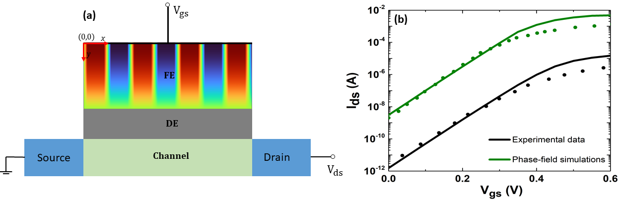
It is well established that the interaction between various energy components determines the state and density of domains in a ferroelectric material [10]-[12],[17]-[26]. Therefore, we follow the same approach to capture both nucleation and motion of the domain wall. In this paper, we present an explicit analytical model of multi-domain FeFET. The 2-D Poisson’s equation is solved with lateral and vertical gradients in the domain polarization. Subsequently, obtained electric field profile is used to calculate the ferroelectric layer’s gradient and depolarization energy density. Net ferroelectric energy (free energy + gradient energy + depolarization energy) is minimized to model the dynamics of multi-domains. Furthermore, the model can capture the secondary effects such as negative capacitance induced by domain wall motion and domain wall transition from soft hard type caused by ferroelectric thickness scaling. The negative capacitance effect is a vital function of domain wall width, which causes variability in the drain current characteristics. Additionally, the experimental results and phase-field simulations thoroughly validate the developed model and algorithm. Fig. 1(a) shows the schematic of an double-gate FeFET with the coordinate axis used in this paper.
2 Development of Electrostatics model with Multi-Domains
The electrostatic model of multi-domain FeFET is mainly divided into four subsections. In the first part, the mathematical formulation of the polarization profile is obtained. Subsequently, the polarization wave model is used in the 2-D Poisson’s equation to derive the 2-D potential functions in the various regions. Afterward, obtained electrostatic model (electric fields and polarization profile) is used to calculate the net ferroelectric energy. Finally, the domain period and dynamics of domains in the ferroelectric region are captured by minimizing net ferroelectric energy.
2.1 Polarization wave model
We assume that polarization of multi-domain in the ferroelectric region is periodic with upward and domain period of and , respectively, and transition from upward to downward domain occurs in the finite domain wall width (). The periodic texture of domains and finite domain wall width are valid approximations observed in experiments and numerical phase-field simulations [10]-[13],[17]-[20]. Therefore, the mathematical formulation of the polarization profile is obtained in Fourier series form.
| (1) |
where, is the total domain period (), is the domain wall width, is the spontaneous polarization and all other Fourier series coefficients are given in the Appendix section.
The y-directional function is included in (1) to incorporate the vertical directional gradient in domain polarization.
| (2) |
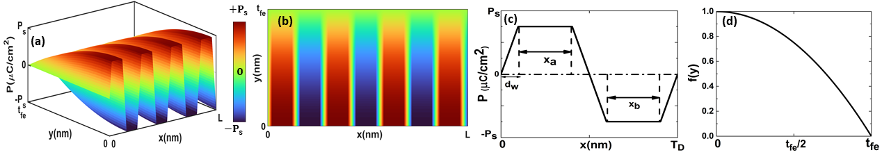
Due to the gradient in polarization along the y-direction, we formulate the function such that: it is maximum at the FE/metal interface (), and it is minimum at the FE/DE interface (). Therefore, the polarization of a domain is maximum at the metal/FE interface and approaches zero at the FE/DE interface (also observed in phase-field simulations, [17], [18]-[20]). Fig. 2 (a) and (b) show polarization’s 3-D and surface distribution in the FE region. Fig. 2(c) shows the schematic of polarization wave with a domain wall width . Fig. 2(d) shows the characteristic of .
2.2 Electrostatic Potential model
Fig. 1(a) shows the schematic diagram of the double gate multi-domain FeFET. The 2-D Poisson’s equation in the various regions is expressed as.
1. Ferroelectric region ()
| (3) |
2. Insulator region ()
| (4) |
3. Channel region ()
| (5) |
This work aims to model the conduction band barrier’s oscillations in a FeFET, which are only significant in the weak inversion region. Therefore, we assume the depletion approximation in the channel . The elementary task is to capture domain nucleation and dynamics in the FE region. Domain dynamics incorporate vertical and lateral gradients in polarization waves (3). The y-directional gradient induces the bound charges () at the FE-DE interface. On the other hand, the lateral gradient in the polarization contributes to domain wall energy density. We will show that various ferroelectric energy components interplay determines a thermodynamically stable domain state in the FE region.
Eq. (3)-(5) are a system of 2-D non-homogeneous partial differential equation (PDE). Green’s function approach obtains the analytical solutions of these equations. Earlier, Green’s function method is used to obtain the 2-D potential distributions of the various DG-MOSFET structures [44]-[51]. In our recent work, an analytical model of MFIS-NCFET is reported[51]. However, the only mono-domain state is considered in the FE region. Hence, the PDE in FE region reduces to a Laplace equation . Therefore, the developed model in [51] cannot capture and study the domain dynamics in the ferroelectric region.
Here, for the first time, we report an analytical and explicit model for multi-domain FeFET with x-y gradients in the polarization (3).
| (6) |
Potential components , and are obtained by following Green’s identity.
| (7) |
| (8) | |||
| (9) | |||
| , and are function of with two series indices , and . | |||
| (10) | |||
| (11) | |||
| , and are function of with series indices | |||
| (12) | |||
| (13) |
Gradients of polarization wave , and are evaluated by (1). Subsequently, evaluated gradients and Green’s functions of the FE region are plugged in (7), which leads to the 2-D potential distributions given by , and , respectively. The remaining two terms originated due to the FE region’s left/right () and top/bottom () boundaries, respectively (given in the Appendix section).
The 2-D potential equations of oxide and channel regions are obtained by using Green’s functions of respective regions into the Green’s identity[44].
| (14) | |||
| (15) |
The mathematical expressions of and approach to calculating lateral Fourier series coefficients are given in the Appendix.
2.3 Energy dynamics in the Ferroelectric material
The equilibrium (applied bias = 0 V) and non-equilibrium (applied bias 0 V) configuration of the domains are determined by minimizing net ferroelectric energy leading to a thermodynamically stable state. The net energy density of the ferroelectric material is given as [11]-[13].
| (16) |
where, is free energy density and expressed in the Taylor series of ferroelectric polarization [11]-[12].
| (17) |
Depolarizing energy density is evaluated by the local distributions of polarization texture and local electric fields [17].
| (18) |
Contributions of local stray fields and polarization in are incorporated by the first and second terms of (18), respectively.
| (19) |
| (20) |
Domain polarization of ferroelectric material exhibits gradients along the spatial and directions [17]-[20]. These gradients in the polarization are incorporated by the and in (3). The gradient energy density of the ferroelectric material is expressed as.
| (21) |
where, the material-dependent ferroelectric coefficients are taken from [26]. We consider a stress-free condition in the Landau coefficients, and strain is incorporated in the Taylor series coefficients of (17). This approximation is validated by the numerical phase-field simulations [18].
2.4 Algorithm to calculate domain period for zero and non-zero applied bias
Firstly, we evaluate the equilibrium domain period () for the zero applied voltages. At zero bias, upward and downward domain, periods will be identical [10]-[13], [17]-[20]. Therefore, the total domain period is calculated as.
| (22) |
The equilibrium domain period is evaluated by minimizing net ferroelectric energy .
| (23) |
where, is the width of device. Typical value of domain wall width is 0.5 nm1 nm [17]-[20]. Hence, after considering an appropriate value of the only unknown in (23) is , which is calculated by the minimization of net ferroelectric energy as.
| (24) |
For a given set of physical parameters such as: , , , , and ferroelectric material parameters (, , etc.) the above equation is an only function of which is solved analytically.
The final task is to evaluate the domain period for non-zero applied voltages (non-equilibrium state). Non-zero applied bias triggers the domain wall motion [17]-[20]. Hence, the period of the upward and downward domain is no longer remains identical (). Depending on the polarity of applied voltage, the expansion/reduction in a domain period is observed. An variation in an upward domain period leads to the same amount of variation in the downward domain period [17]-[20]. Therefore, the total domain period remains the same as in an equilibrium condition period (22).
| (25) |
However, due to the non-equilibrium condition, , and the amount of shift is given by , which is calculated by the minimization of net ferroelectric energy.
| (26) |
Domain dynamics is captured by plugging (For each applied voltages) in (6).
3 Results and Discussion
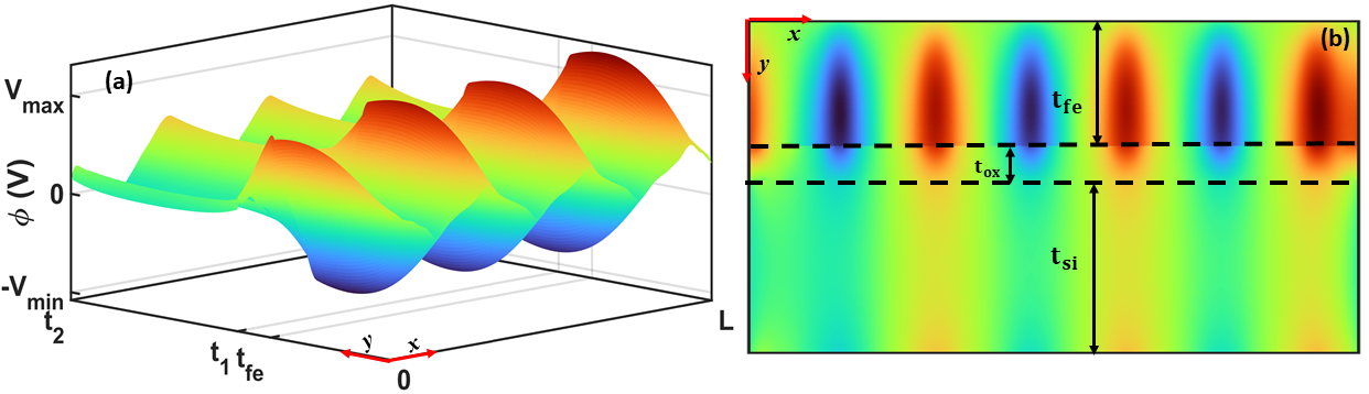
To check the robustness and accuracy of the model, we consider both types of validations: numerical simulations and experimental results. Fig. 1(b) shows validations of the developed model against phase-field simulations [26], and experimental results [27]. Fig. 3 shows the electrostatic potential distribution (at zero bias) of a FeFET with multi-domains. Due to the adjacent periodic nature of polarization charges in the FE region (see 2(a)), the electrostatic of the device also exhibits periodicity. The value of (difference between maximum and minimum values of the potential) is 500 mV and 40 mV at the metal/FE () interface and at the mid-channel , respectively. Such significant variations in the channel potential will exponentially alter the thermionic current transport.
3.1 Negative Capacitance via Domain wall motion
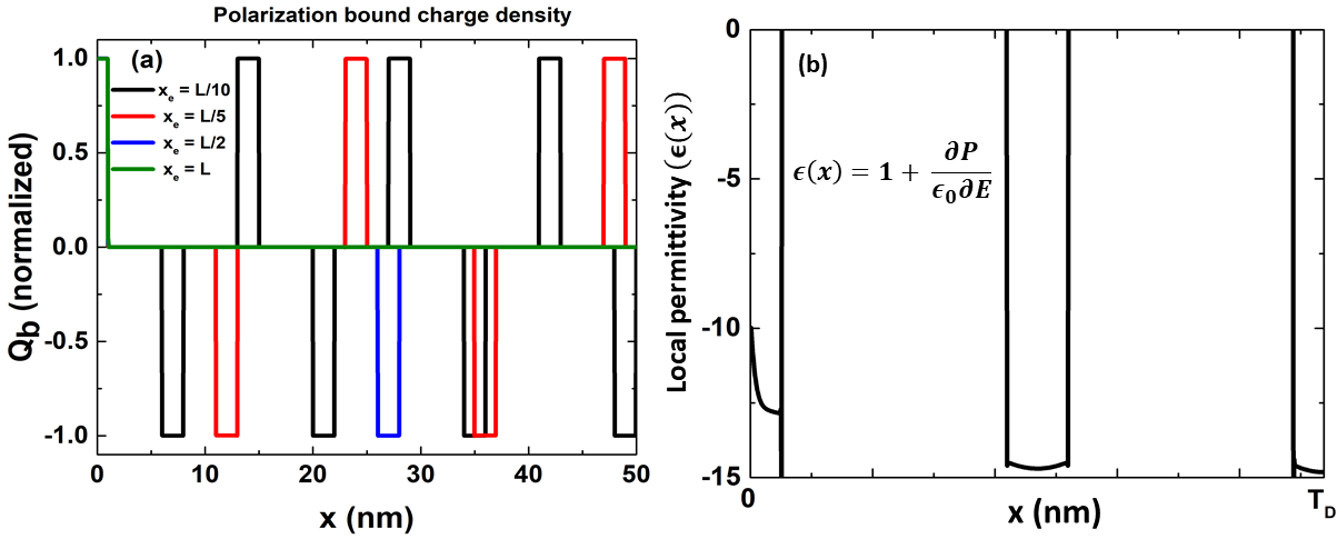
The lateral gradient of polarization profile in (3) induces the bound charge density along the lateral direction. Fig. 4(a) shows the bound charge density () distribution in the FE region for various domain periods. Charge density exhibits the periodic nature with positive and negative values. Fig. 4(b) shows the local permittivity of the FE region (for a domain period = ), which is calculated by the electric displacement vector. The emergence of negative permittivity is observed due to the negative slope of polarization vector w.r.t. electric field vector . The signature of negative permittivity is the origin of negative capacitance induced by domain wall motion. Note that, recently, an experimental study also demonstrated the presence of NC by domain dynamics in a ferroelectric capacitor [25]. Therefore, the developed model can capture inherent negative capacitance by domain wall motion.
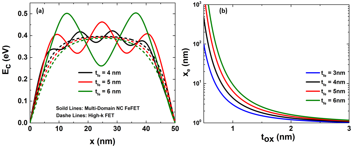
Fig. 5(a) shows the conduction band profile plotted at the middle of the channel for various values. Due to enhanced fringing fields, the negative capacitance effect shoots up as ferroelectric thickness increases [33]. Therefore, the barrier height in the conduction band rises with an increasing . The number of domains in the FE region is determined by the interactions in various energy components given by (16). An enhancement in corresponds to a wider dispersion in domain polarization along the vertical direction. Therefore, the slope of decreases (see Fig. 2(d)), which reduces gradient energy density along the y-direction. This reduction in the gradient energy relaxes the compulsion to nucleate denser domain patterns for achieving energy minima. Now, energy can be minimized by the lesser number of domains. Hence, the domain period increases, which reduces the rate of oscillations in the conduction band, as shown in Fig. 5(a). On the other hand, as increases, the depolarizing fields increases [10],[17]-[20], [24]. Therefore, more number domains nucleates to compensate for the increased depolarizing energy, as shown in Fig. 5(b). Note that similar kinds of observations were also reported in a pioneer work by Bratkovsky et al. [10], and the phase-field simulations [17]-[20]. Therefore, Fig. 5(b) shows a further validation of the developed model and algorithm to capture nucleation of domains in the FE region.
3.2 Electronic transport with multi-domains
The drain to source current is calculated by the Quasi-Fermi potential of the channel [51].
| (27) |
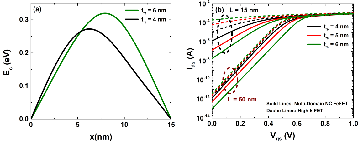
Fig. 6(a) shows a short channel device’s conduction band energy plot (L = 15 nm). The number of domain walls varies with the variations in (see Fig. 5). Hence, the position of local NC shifts with the alteration in . Thus, the maximum barrier height of the conduction band exhibits a positional variation with ferroelectric thickness. Shifting in the barrier height signifies the presence of a domain wall at that particular position. Additionally, enhancement in the barrier height with a larger is due to the increased NC effect. Fig. 6(b) shows the characteristics of a FeFET. Solid curves are used for FeFET with multi-domains which includes the negative capacitance effect (due to the domain wall motion), and dashed curves are plotted for the conventional high-k FET where the domain wall does not exist (hence, the NC effect is absent). Enhancement in the raises the conduction band barrier height (see Fig. 5(a) and Fig. 6(a)), which leads to a reduction in OFF current (NC effect gets stronger with the larger value of ). On the other hand, conventional high-k FET exhibits the reverse trend with , as shown in Fig. 5(a) (dashed curves). The barrier height reduces with an increment in the FE layer thickness. Therefore, the OFF current value rises with an increasing value of .
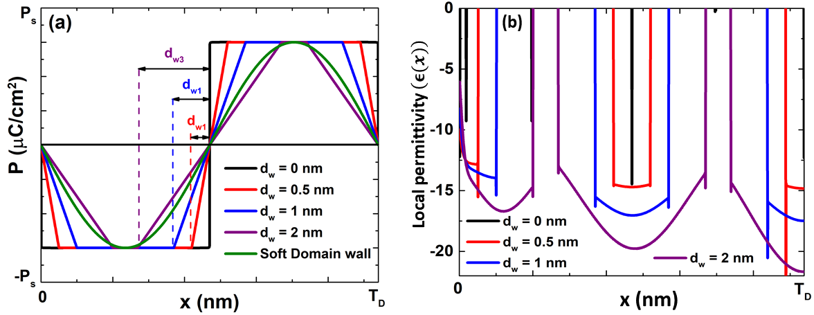
3.3 Soft Hard domain wall transition
The phase-field simulations demonstrated that scaling in the FE layer triggers a domain wall transition from hard to soft type [18]-[20], [26]. This second order effect is incorporated in the model by transforming the polarization profile in the FE layer. Fig. 7(a) shows the polarization profile with the variations in domain wall width (). The hard domain wall texture is observed at . However, a gradual enhancement in leads to a soft domain wall transition. Therefore, transition of the domain wall with can be incorporated by defining a parameter .
| (28) |
can be tuned to capture soft/hard domain wall transitions, and is the starting domain period (without transition). Impact of domain wall transition on negative permittivity is shown in Fig. 7(b). The magnitude of local permittivity increases with the larger , which can be understood by analyzing the ratio.
| (29) |
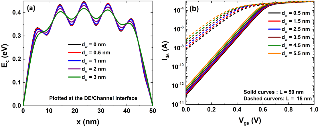
An increase in reduces ratio (see Fig. 7(a)), however, the ratio also decreases with the larger . A larger permittivity value with the states that the electric field vector is more sensitive than the polarization vector for spatial variations . An alternative explanation for increased permittivity with can be understood by observing the conduction band profile, as shown in Fig. 8(a). As increases, the barrier height decreases. Thus, the NC’s strength reduces with the larger . The strength of negative capacitance is inversely proportional to the ferroelectric layer capacitance , a larger value of deteriorates the capacitance matching leading to a weaker NC effect [Khan]-[36]. Since a larger magnitude of local permittivity enhances the value, the barrier height decreases with the increasing . Therefore, the transition towards the soft domain wall increases the sub-threshold current, as observed in Fig. 8(b). Note that variability is higher in the short channel device (L = 15 nm) than the long channel device (L = 50 nm). This may be attributed to the fact that the SCEs dominate at smaller channel lengths, which further reduces the impact of the NC effect, leading to a higher variability.
.
4 Conclusion
An analytical physics-based model of multi-domain FeFET is developed by solving 2-D Poisson’s equation with the ferroelectric energy dynamics state equation. The process of domain wall nucleation and motion occurs to minimize the net system energy. The dynamics of multi-domains (nucleation of a new domain and domain wall motion) are captured by minimizing net system energy. Ferroelectric energy directly depends on physical parameters such as and . Hence, the domain period can be engineered by the alterations in the FE physical parameters. The motion of domain wall leads to the origination of local negative permittivity in the FE layer. A wider domain wall enhances the magnitude of local permittivity leading to a weaker negative capacitance effect. Furthermore, the transition of domain wall softhard introduces variability in the characteristics.
References
- [1] T. S. Boscke, J. Muller, D. Brauhaus, U. Schroder, and U. Bottger, “Ferroelectricity in hafnium oxide: CMOS compatible ferroelectric field effect transistors,” in IEDM Tech. Dig., Dec. 2011, pp. 24.5.1–24.5.4, doi: 10.1109/IEDM.2011.6131606.
- [2] S. Mueller, J. Mueller, A. Singh, S. Riedel, J. Sundqvist, U. Schroeder, and T. Mikolajick, “ Incipient ferroelectricity in Al-doped HfO2 thin films,” Adv. Funct. Mater. 22, 2412–2417 (2012). https://doi.org/10.1002/adfm.201103119.
- [3] J. Mu¨ller, T. S. Böscke, U. Schröder, S. Mueller, D. Brauhaus, U. Böttger, L. Frey, and T. Mikolajick, “ Ferroelectricity in simple binary ZrO2 and HfO2,” Nano Lett. 12, 4318 (2012). https://doi.org/10.1021/nl302049k.
- [4] S. Fujii et al., “First demonstration and performance improvement of ferroelectric HfO2-based resistive switch with low operation current and intrinsic diode property,” in Proc. VLSI Tech. Symp., 2016, pp. 1–2.
- [5] M. Trentzsch et al. A 28 nm HKMG super low power embedded NVM technology based on ferroelectric FETs, in IEEE International Electron Devices Meeting (2016), pp. 294–297.
- [6] J. Muller, T. S. Boscke, U. Schroder, R. Hoffmann, T. Mikolajick, and L. Frey, “Nanosecond polarization switching and long retention in a novel MFIS-FET based on ferroelectric HfO2,” IEEE Electron Device Lett., vol. 33, no. 2, pp. 185–187, Feb. 2012, doi: 10.1109/ LED.2011.2177435.
- [7] E. T. Breyer, H. Mulaosmanovic, T. Mikolajick, and S. Slesazeck, “Reconfigurable NAND/NOR logic gates in 28 nm HKMG and 22 nm FD-SOI FeFET technology,” in IEDM Tech. Dig., Dec. 2017, pp. 28.5.1–28.5.4, doi: 10.1109/IEDM.2017.8268471.
- [8] H. Mulaosmanovic et al., “Evidence of single domain switching in hafnium oxide based FeFETs: Enabler for multi-level FeFET memory cells,” in IEDM Tech. Dig., vol. 3, Dec. 2015, pp. 26.8.1–26.8.3, doi: 10.1109/IEDM.2015.7409777.
- [9] K. Florent et al., “Vertical ferroelectric HfO2 FET based on 3-D NAND architecture: Towards dense low-power memory,” in IEDM Tech. Dig., Dec. 2018, pp. 2–5, doi: 10.1109/IEDM.2018.8614710.
- [10] A. M. Bratkovsky, & A. P. Levanyuk, Abrupt appearance of the domain pattern and fatigue of thin ferroelectric films. Phys. Rev. Lett. 84, 3177–3180, https://doi.org/10.1103/PhysRevLett.84.3177 (2000).
- [11] M. E. Lines, & A. M. Glass, Principles and Applications of Ferroelectrics and Related Materials (Clarendon Press, Oxford, 1977).
- [12] K. M. Rabe, C. H. Ahn & J. M. Triscone, Physics of Ferroelectrics: a Modern Perspective Vol. 105, Springer Science & Business Media (2007).
- [13] I. Luk’yanchuk, , A. Sené, & V. M. Vinokur, Electrodynamics of ferroelectric films with negative capacitance. Phys. Rev. B 98, 024107 (2018).
- [14] Anna N. Morozovska et al. Interaction of a 180° ferroelectric domain wall with a biased scanning probe microscopy tip: Effective wall geometry and thermodynamics in Ginzburg-Landau-Devonshire theory. Phys. Rev. B 78 (2008), 125407, https://doi.org/10.1103/PhysRevB.78.125407.
- [15] E. A. Eliseev, A. N. Morozovska, S. V. Kalinin, Y. L. Li, Jie Shen, M. D. Glinchuk, L. Q. Chen, and V. Gopalan, Surface Effect on Domain Wall Width in Ferroelectrics, J. Appl. Phys. 106, 084102 (2009).
- [16] I. A. Luk’yanchuk, L. Lahoche, & A. Sene, Universal Properties of Ferroelectric Domains. Phys. Rev. Lett. 102, 10.1103/PhysRevLett.102.147601 (2009).
- [17] H. W. Park, J. Roh, Y. B. Lee & C. S. Hwang, Modeling of negative capacitance in ferroelectric thin films, Adv. Mater., vol. 31, Jun. 2019.
- [18] A.K. Saha, S.K. Gupta, Multi-Domain Negative Capacitance Effects in Metal-Ferroelectric-Insulator-Semiconductor/Metal Stacks: A Phase-field Simulation Based Study. Sci Rep 10, 10207 (2020). https://doi.org/10.1038/s41598-020-66313-1.
- [19] A. K. Saha, M. Si, K. Ni, S. Datta, P. D. Ye, and S. K. Gupta, “Ferroelectric thickness dependent domain interactions in FEFETs for memory and logic: A phase-field model based analysis,” in IEEE International Electron Devices Meeting (IEDM) (IEEE, San Francisco, CA, 2020), pp. 4.3.1–4.3.4.
- [20] A. K. Saha & S. K. Gupta, Negative capacitance effects in ferroelectric heterostructures: A theoretical perspective”, J. Appl. Phys., vol. 129, no. 8, Feb. 2021.
- [21] M. Hoffmann, et al., On the stabilization of ferroelectric negative capacitance in nanoscale devices. Nanoscale 10, 10891–10899 (2018).
- [22] M. Hoffmann, et al., Unveiling the double-well energy landscape in a ferroelectric layer. Nature 565, 464–467 (2019). https://doi.org/10.1038/s41586-018-0854-z.
- [23] P. Zubko, et al., Negative capacitance in multidomain ferroelectric superlattices. Nature 534, 524–528 (2016).
- [24] A. M. Bratkovsky, & A. P. Levanyuk, Very large dielectric response of thin ferroelectric films with the dead layers. Phys. Rev. B 63, 132103, https://doi.org/10.1103/PhysRevB.63.132103 (2001).
- [25] A. K. Yadav, et al., Spatially resolved steady-state negative capacitance. Nature 565, 468–471 (2019).
- [26] A. K. Saha and S. K. Gupta, ”Multi-Domain Ferroelectric FETs with Negative and Enhanced Positive Capacitance for Logic Applications,” 2021 International Conference on Simulation of Semiconductor Processes and Devices (SISPAD), 2021, pp. 77-80, doi: 10.1109/SISPAD54002.2021.9592573.
- [27] Z. Krivokapic et al., ”14nm Ferroelectric FinFET technology with steep subthreshold slope for ultra low power applications,” 2017 IEEE International Electron Devices Meeting (IEDM), 2017, pp. 15.1.1-15.1.4, doi: 10.1109/IEDM.2017.8268393.
- [28] S. Salahuddin and S. Datta, “Use of negative capacitance to provide voltage amplification for low power nanoscale devices,” Nano Lett., vol. 8, no. 2, pp. 405–410, 2007, doi: 10.1021/nl071804g.
- [29] G. A. Salvatore, D. Bouvet, and A. M. Ionescu, “Demonstration of subthrehold swing smaller than 60mV/decade in Fe-FET with P(VDF-TrFE)/SiO2 gate stack,” in IEDM Tech. Dig., Dec. 2008, pp. 1–4, doi: 10.1109/IEDM.2008.4796642.
- [30] M. Kobayashi and T. Hiramoto, “Device design guideline for steep slope ferroelectric FET using negative capacitance in sub-0.2V operation: Operation speed, material requirement and energy efficiency,” in VLSI Symp. Tech. Dig., Jun. 2015, pp. T212–T213, doi: 10.1109/VLSIT.2015.7223678.
- [31] H. Ota, T. Ikegami, J. Hattori, K. Fukuda, S. Migita, A. Toriumi, ”Fully coupled 3-D device simulation of negative capacitance FinFETs for sub 10 nm integration”, IEDM Tech. Dig., pp. 12.4.1-12.4.4, Dec. 2016, DOI: 10.1109/IEDM.2016.7838403
- [32] W. Cao, , K Banerjee, Is negative capacitance FET a steepslope logic switch?. Nat Commun 11, 196 (2020). DOI: https://doi.org/10.1038/s41467-019-13797-9
- [33] G. Pahwa, A. Agarwal, Y. S. Chauhan, ”Numerical investigation of short-channel effects in negative capacitance MFIS and MFMIS transistors: Subthreshold behavior”, IEEE Trans. Electron Devices, vol. 65, no. 11, pp. 5130-5136, Nov. 2018, DOI: 10.1109/TED.2018.2870519.
- [34] G. Pahwa et al., ”Analysis and Compact Modeling of Negative Capacitance Transistor with High ON-Current and Negative Output Differential Resistance—Part II: Model Validation,” in IEEE Transactions on Electron Devices, vol. 63, no. 12, pp. 4986-4992, Dec. 2016, doi: 10.1109/TED.2016.2614436.
- [35] G. Pahwa et al., ”Compact Model for Ferroelectric Negative Capacitance Transistor With MFIS Structure,” in IEEE Transactions on Electron Devices, vol. 64, no. 3, pp. 1366-1374, March 2017, doi: 10.1109/TED.2017.2654066.
- [36] G. Pahwa et al., ”Physical Insights on Negative Capacitance Transistors in Nonhysteresis and Hysteresis Regimes: MFMIS Versus MFIS Structures,” in IEEE Transactions on Electron Devices, vol. 65, no. 3, pp. 867-873, March 2018, doi: 10.1109/TED.2018.2794499.
- [37] X. Zhang et al., “Analysis on performance of ferroelectric NC-FETs based on real-space Gibbs-free energy with atomic channel structure,” IEEE Trans. Electron Devices, vol. 66, no. 2, pp. 1100-1106, 2019.
- [38] Asif Islam Khan, et al. ”Negative capacitance in a ferroelectric capacitor.” Nature materials 14.2 (2015): 182.
- [39] Ku, Hansol, and Changhwan Shin. ”Transient response of negative capacitance in P (VDF 0.75- TrFE 0.25) organic ferroelectric capacitor.” IEEE Journal of the Electron Devices Society 5.3 (2017): 232-236.
- [40] M. Hoffmann, B. Max, T. Mittmann, U. Schroeder, S. Slesazeck and T. Mikolajick, ”Demonstration of High-speed Hysteresis-free Negative Capacitance in Ferroelectric Hf0.5Zr0.5O2,” 2018 IEEE International Electron Devices Meeting (IEDM), San Francisco, CA, 2018, pp. 31.6.1-31.6.4.
- [41] Daniel JR Appleby, et al. ”Experimental observation of negative capacitance in ferroelectrics at room temperature.” Nano letters 14.7 (2014): 3864-3868.
- [42] A. Cano and D. Jiménez, “Multidomain ferroelectricity as a limiting factor for voltage amplification in ferroelectric field-effect transistors,” Appl. Phys. Lett., vol. 97, no. 13, p. 133509, 2010.
- [43] S. Kasamatsu, S. Watanabe, C. S. Hwang, and S. Han, “Emergence of negative capacitance in multidomain ferroelectric—Paraelectric nanocapacitors at finite bias,” Adv. Mater., vol. 28, no. 2, pp. 335–340, 2016.
- [44] J. D. Jackson, Classical Electrodynamics3rd edn, chapter-1, (Wiley, (1999)).
- [45] P.-S. Lin and C.-Y. Wu, “A new approach to analytically solving the two-dimensional Poisson’s equation and its application in short-channel MOSFET modeling,” IEEE Trans. Electron Devices, vol. ED-34, no. 9, pp. 1947–1956, Sep. 1987.
- [46] J.-Y. Guo and C.-Y. Wu, “A new 2-D analytic threshold-voltage model for fully depleted short-channel SOI MOSFETs,” IEEE Trans. Electron Devices, vol. 40, no. 9, pp. 1653–1661, Sep. 1993, DOI: 10.1109/16.231571.
- [47] A. Nandi, N. Pandey, S. Dasgupta, ”Analytical modeling of DG-MOSFET in subthreshold regime by green’s function approach”, IEEE Trans. Electron Devices, vol. 64, no. 8, pp. 3056-3062, Aug. 2017, 10.1109/TED.2017.2708603.
- [48] A. Nandi and N. Pandey, “Accurate analytical modeling of junctionless DG-MOSFET by Green’s function approach,” Superlattices Microstruct., vol. 111, pp. 983–990, Nov. 2017, doi: 10.1016/j. spmi.2017.07.062.
- [49] A. Nandi, N. Pandey and S. Dasgupta, ”Analytical Modeling of Gate-Stack DG-MOSFET in Subthreshold Regime by Green’s Function Approach,” in IEEE Transactions on Electron Devices, vol. 65, no. 10, pp. 4724-4728, Oct. 2018.
- [50] N. Pandey, H.-H. Lin, A. Nandi, and Y. Taur, “Modeling of short-channel effects in DG MOSFETs: Green’s function method versus scale length model,” IEEE Trans. Electron Devices, vol. 65, no. 8, pp. 3112–3119, Aug. 2018, DOI: 10.1109/TED.2018.2845875.
- [51] N. Pandey and Y. S. Chauhan, ”Analytical Modeling of Short-Channel Effects in MFIS Negative-Capacitance FET Including Quantum Confinement Effects,” in IEEE Transactions on Electron Devices, vol. 67, no. 11, pp. 4757-4764, Nov. 2020, doi: 10.1109/TED.2020.3022002.
Appendix
, and are calculated by the potential continuity condition at FE/DE, and DE/channel interface respectively.
| (30) |
Note that, the dynamics of multi-domains introduces Fourier coefficient in the above equations.
| (31) | |||
| (32) | |||
| (33) |
Fourier series coefficients: are evaluated by multiplying sin in the potential functions and integrating from 0 to L. Where, .
are the Fourier series coefficients with and indices.
| (34) | |||
| (35) | |||
| (36) |
| (37) | |||
| (38) | |||
| (39) | |||
| (40) | |||
| (41) | |||
| (42) | |||
| (43) | |||
| (44) | |||
| (45) | |||
| (46) | |||
| (47) | |||
| (48) | |||
| (49) | |||
| (50) | |||
| where, , and are the Fourier coefficients evaluated at the oxide gaps. | |||
| (51) | |||
| (52) | |||
| , are calculated by the same manner by replacing with . | |||
| Green’s function for the various region are derived in our earlier work[51]. |