Universal control of a six-qubit quantum processor in silicon
Future quantum computers capable of solving relevant problems will require a large number of qubits that can be operated reliably. However, the requirements of having a large qubit count and operating with high-fidelity are typically conflicting. Spins in semiconductor quantum dots show long-term promise but demonstrations so far use between one and four qubits and typically optimize the fidelity of either single- or two-qubit operations, or initialization and readout. Here we increase the number of qubits and simultaneously achieve respectable fidelities for universal operation, state preparation and measurement. We design, fabricate and operate a six-qubit processor with a focus on careful Hamiltonian engineering, on a high level of abstraction to program the quantum circuits and on efficient background calibration, all of which are essential to achieve high fidelities on this extended system. State preparation combines initialization by measurement and real-time feedback with quantum-non-demolition measurements. These advances will allow for testing of increasingly meaningful quantum protocols and constitute a major stepping stone towards large-scale quantum computers.
On the path to practical large-scale quantum computation, electron spin qubits in semiconductor quantum dots [1] show promise due to their inherent potential for scaling through their small size [2, 3], long-lived coherence [4] and compatibility with advanced semiconductor manufacturing techniques [5]. Nevertheless, spin qubits currently lag behind in scale when compared to superconducting, trapped ions and photonic platforms, which have demonstrated control of several dozen qubits [6, 7, 8]. By comparison, using semiconductor spin qubits, control of up to four qubits was achieved [9] and entanglement of up to three qubits was quantified [10, 11, 12].
Furthermore, the experience with other qubit platforms shows that in scaling up, maintaining the quality of the control requires significant efforts, for instance to deal with the denser motional spectrum in trapped ions [13], to avert cross-talk in superconducting circuits [14] or to avoid increased losses in photonic circuits [15]. For small semiconductor spin qubit systems, state-of-the-art single-qubit gate fidelities exceed 99.9% [16, 17, 18] and two-qubit gates well above 99% fidelity have been demonstrated recently [19, 20, 21, 11]. Most quantum dot based demonstrations suffer from rather low initialization or readout fidelities, with typical visibilities of no more than 60-75%, with one recent exception [21]. Conversely, high-fidelity spin readout has been claimed based on an analysis of the readout error mechanisms, but these claims have not been validated in combination with high-fidelity qubit control [22, 23]. While high-fidelity initialization, readout, single-qubit gates and two-qubit gates have thus been demonstrated individually in small systems, almost invariably one or more of these parameters are significantly comprised while optimizing others. A major challenge and important direction for the field is therefore to achieve high fidelities for all components while at the same time enlarging the qubit count.
Here we study a system of six spin qubits in a linear quantum dot array and test what performance can be achieved using known methods such as multi-layer gate patterns for independent control of the two-qubit exchange interaction [24, 25, 26] and micromagnet gradients for electric-dipole spin resonance and selective qubit addressing [27]. Furthermore, we introduce several novel techniques for semiconductor qubits that, collectively, are critical to improve on the results and facilitate scalability, such as initialization by measurement using real-time feedback [28], qubit initialization and measurement without reservoir access, and efficient calibration routines. Initialization and readout circuits span over the full six-qubit array. We characterize the quality of the control by preparing maximally entangled states of two and three spins across the array.
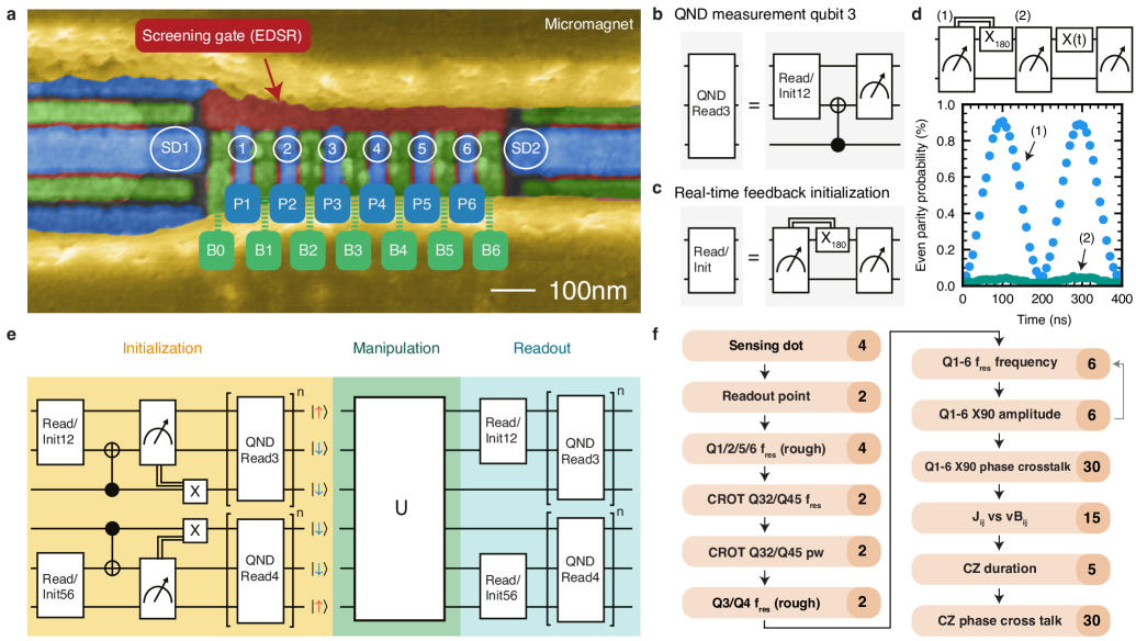
The six-qubit array is defined electrostatically in the 28Si quantum well of a 28Si/SiGe heterostructure, between two sensing quantum dots, as seen in Figure 1a (see Methods). The multi-layer gate pattern allows for excellent control of the charge occupation of each quantum dot, and of the tunnel couplings between neighbouring quantum dots. These parameters are controlled independently through linear combinations of gate voltages, known as virtual gates [29]. The inter-dot pitch is chosen to be 90 nm, which for this 30 nm deep quantum well yields easy access to the regime with one electron in each dot, for short indicated as the (1,1,1,1,1,1) charge occupation. Low valley splittings on Si/SiGe devices have hindered progress in the past [30], but in this device all valley splittings are in the range of 100-300 µeV (See Supplementary materials).
In designing the qubit measurement scheme, we focused on achieving short measurement cycles in combination with high-fidelity readout, as this accelerates testing of all other aspects of the experiment. For measuring the outer qubit pairs, we use Pauli-Spin blockade (PSB) to probe the parity of the two spins (rather than differentiating between singlet and triplet states), exploiting the fact that the T0 triplet relaxes to the singlet well before the end of the 10 µs readout window. We tune the outer dot pairs of the array to the (3,1) electron occupation, where the readout window is larger than in the (1,1) regime (see Extended Data 1). Since the sensing dots are less sensitive to the charge transition between the center dots, the middle qubits are measured by quantum-non-demolition (QND) measurements that map the state of qubit 3(4) on qubit 2(5) via a conditional rotation (CROT) (Fig. 1b) [16, 31]. In this way, for every iteration of the experiment, 4 bits of information are retrieved which depend on the state of all 6 physical qubits. Iterative operation permits full readout of the 6-qubit system.
Qubit initialization is based on measurements of the spin state across the array followed by real-time feedback to place all qubits in the target initial state. This scheme has the benefit of not relying on slow thermalization and that no access to electron reservoirs is needed to bring in fresh electrons, which is helpful for scaling to larger arrays. In fact, we had experiment runs of more than one month in which the electrons stayed within the array continuously. For qubits 3 and 4, real-time feedback simply consists of flipping the qubit if the measurement returned . Initialization of qubits 1-2 (or 5-6) using parity measurements and real-time feedback is illustrated in Figure 1d. First, assuming that the qubits start from a random state, we perform a parity measurement that will cause the state to either collapse to an even (, ) or odd (/) parity (see Methods). After the measurement, a pulse is applied to qubit 1 in case of even parity, which converts the state to odd parity (feedback latency 660 ns). Subsequently, we perform a second measurement, which converts either of the odd parity states to . Specifically, when pulsing towards the readout operating point, both and relax into the singlet state ((4,0) charge occupation). When pulsing adiabatically from the (4,0) back to the (3,1) charge configuration, the singlet is mapped onto the state. If the qubit initialization is successful, the second measurement should return an odd parity (typically 95% success rate). To further boost the initialization fidelity we use the outcome of the second measurement to post-select successful experiment runs (see Extended Data Fig. 1d). Figure 1d shows initialization by measurement of the first two qubits. The first readout outcome (blue) shows Rabi oscillations controlled by a microwave burst of variable duration applied near the end of the previous cycle (see methods for more details). The second readout outcome (green) shows the state after the real-time classical feedback step. The oscillation has largely vanished, indicating successful initialization by measurement and feedback.
The sequence to initialize and measure all qubits is shown in Figure 1e (see Extended Data 2 for the unfolded quantum circuit). We sequentially initialize qubit pair 5-6, then qubit 4, then qubits 1-2, and finally qubit 3, using the steps described above (for compactness, the steps appear as simultaneous in the diagram). In order to further enhance the measurement and initialization fidelities, we repeat the QND measurement three times, alternating the order of qubit 3 and 4 measurements. We post-select runs with three identical QND readout outcomes in both the initialization and measurement steps (except for Fig. 5 below, where readout simply uses majority voting). After performing the full initialization procedure depicted in Fig. 1e, the six qubit array is initialized in the state . In all measurements below, we initialize either two, three or all six qubits, depending on the requirement of the specific quantum circuit we intend to run. We leave the unused qubits randomly initialized, as the visibilities decrease when initializing all 6 qubits within a single shot sequence (see Extended Data 3). When operating on individual qubits, the initialization and measurement procedures yield visibilities of 93.5-98% (see Fig. 2e). To put these numbers in perspective, if the readout error for both and were 1% alongside an initialization error of 1%, the visibility would be 96%.
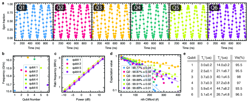
We manipulate the qubits via electric-dipole spin resonance (EDSR) [32]. A micromagnet located above the gate-stack is designed to provide both qubit addressability and a driving field gradient (see Fig. 1a and Supplementary Data). We can address each qubit individually and drive coherent Rabi oscillations as depicted in figure 2. We observe no visible damping in the first five periods. The data in figure 2c shows that the qubit frequencies are not spaced linearly, deviating from our prediction based on numerical simulations of the magnetic field gradients (Supplementary Figure 1). However, the smallest qubit frequency separation of 20 MHz is sufficient for selective qubit addressing with our operating speeds varying between 2 MHz and 5 MHz. The Rabi frequency is linear in the driving amplitude over the typical range of microwave power used in the experiment (Fig. 2c). We operate single-qubit gates sequentially, to ensure we stay in this linear regime and to keep the calibration simple. We characterize the single-qubit properties of each qubit separately. Figure 2d shows results of randomized benchmarking experiments. All average single-qubit gate fidelities are between 99.77% 0.04 and 99.96% 0.01, which demonstrates that even within this extended qubit array, we retain high-fidelity single-qubit control. The coherence times of each qubit are tabulated in figure 2e. We expect spin coherence to be limited by charge noise coupling in by the micromagnet [33].
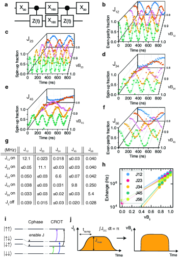
Two-qubit gates are implemented by pulsing the (virtual) barrier gate between adjacent dots while staying at the symmetry point. Pulsing the barrier gate leads to a ZZ interaction (throughout, X, Y and Z stand for the Pauli operators, I for the identity, and ZZ is shorthand for the tensor product of two Pauli Z operators, etc), given that the effect of the flip-flop terms of the spin exchange interaction is suppressed due to the differences in the qubit splittings [36]. The quantum circuit in Fig. 3a measures the time evolution under the ZZ component of the Hamiltonian only, as the single-qubit pulses in between the two exchange pulses decouple any IZ/ZI terms [37]. The measured signal oscillates at a frequency (Fig. 3b-f) as a function of the barrier gate pulse duration, corresponding to Controlled Phase (CPhase) evolution. When pulsing only the barrier gate between the target qubit pair, the desired on/off ratio of (>100) could not be achieved. We solve this, without sacrificing operation at the symmetry point, by using a linear combination of the virtual barrier gates (vB1-vB6). Specifically, the barrier gates around the targeted quantum dot pair are pulsed negatively to push the corresponding electrons closer together and thereby enhance the exchange interaction (see Extended Data Fig. 1). The exponential dependence of on virtual barrier gates is seen in Fig. 3h. In Fig. 3g we investigate the residual exchange of idle qubit pairs, while one qubit pair is pulsed to its maximal exchange value within the operating range. The results show minimal residual exchange amplitudes in the off-state between the other pairs.
Through suitable timing, we use the CPhase evolution to implement a Controlled-Z (CZ) gate. Fig. 3j shows the pulse shape that is used to ensure a high degree of adiabaticity throughout the CZ gate [19]. We use a Tukey window as waveform, with a ramp time of [38]. This pulse shape is defined in units of energy and we convert it into barrier voltages using the measured voltage to exchange energy relation [19].
One of the challenges when operating larger quantum processors is to track and compensate any dynamical changes in qubit parameters to ensure high-fidelity operation, initialization and readout. Another challenge is to keep track of and compensate for cross-talk effects imparted by both single- and two-qubit gates on the phase evolution of each qubit. We perform automated calibrations, as shown in Fig. 1f, and correct 108 parameters in total. The detailed description of each calibration routine is included in the methods section and Extended Data Fig. 4. Twice a week, we run the full calibration scheme, which takes about one hour. Every morning, we run the calibration scheme leaving out the phase corrections for single-qubit operations and the dependence of on the virtual barrier gates vBij. Sometimes, specific calibrations, especially qubit frequencies and readout coordinates, are rerun throughout the day, as needed. Supplementary Data figure 3 plots the evolution of the calibrated values for a number of qubit parameters over the course of one month.
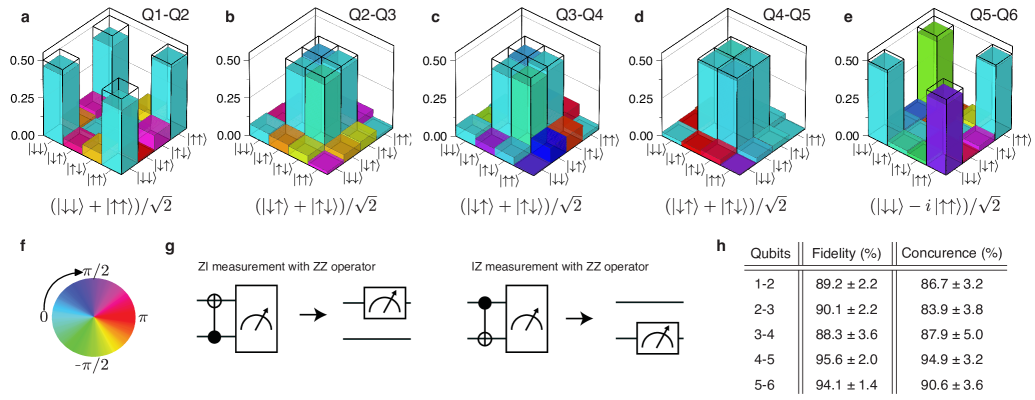
With single- and two-qubit control established across the six-qubit array, we proceed to create and quantify pairwise entanglement across the quantum dot array as a measure of the quality of the qubit control (Fig. 4a-e). These experiments benefited from a high level of abstraction in the measurement software, allowing us to flexibly program a variety of quantum circuits acting on any of the qubits, drawing on the table of 108 calibration parameters that is kept updated in the background and on the detailed waveforms to achieve high-fidelity gates. The parity readout of the outer qubits yields a native ZZ measurement operator. We measure single-qubit expectation values by mapping the ZZ operator to a ZI/IZ operator, as shown in figure 4g. This allows full reconstruction of the density matrix. The state fidelity is calculated using , where is the target state and is the measured density matrix. The target states are maximally entangled Bell states. The obtained density matrices measured across the six-dot array have a state fidelity ranging from 88% to 96%, which is considerably higher than the Bell state fidelities of 78% to 89% reported on two-qubit quantum dot devices just a few years ago [37, 35, 39].
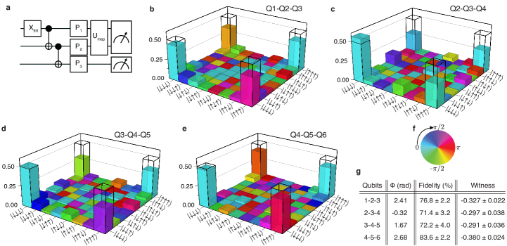
As a final characterization of the qubit control across the array, we prepare Greenberger–Horne–Zeilinger (GHZ) states, which are the most delicate entangled states of three qubits [40, 41]. Fig. 5a shows the quantum circuit we used to prepare the GHZ states. The full circuit, including initialization and measurement, contains up to 14 CROT operations, 2 CZ operations, 42 parity measurements, 16 single-qubit rotations conditional on real-time feedback, and 5 single-qubit X90 rotations (see Extended Data Fig. 2). The measurement operators for quantum state tomography are generated in a similar manner as for the Bell states. In order to reconstruct three-qubit density matrices, we perform measurements in 26 (for qubits 234 and 345) or 44 (for qubit 123 and 456) different basis and repeat each set 2000 times to collect statistics. A full dataset consisting of 52000 (88000) single-shot repetitions takes about 5 minutes to acquire, thanks to the efficient uploading of waveforms to the waveform generator (see Methods) and the short single-shot cycle times. Figs. 5b-e show the measured density matrices for qubits 123, 234, 345 and 456. The obtained state fidelities range from 71% to 84% (see Methods for a brief discussion of dephasing effects from heating). For comparison, the record GHZ state fidelity reported recently for a triple quantum dot spin qubit system is 88% [10]. The same data set from [10] analyzed without readout correction yields 45.8% fidelity, while our results with no readout error removal range from 52.8% to 67.2% (see Supplementary Data). From the same data sets, we calculate entanglement witnesses, which clearly demonstrate three-qubit entanglement (see Supplementary Data).
The demonstration of universal control of six qubits in a 28Si/SiGe quantum dot array advances the field in multiple ways. While scaling to a record number of qubits for a quantum dot system, we achieve Rabi oscillations for each qubit with visibilities of 93.5-98%, implying high readout and initialization fidelities. Initialization uses a novel scheme relying on qubit measurement and real-time feedback. Readout relies on Pauli spin blockade and quantum-non-demolition measurements. This combination of initialization and readout allows to the device to be operated while retaining the six electrons in the linear quantum dot array, alleviating the need for access to electron reservoirs. All single-qubit gate fidelities are around 99.9% and the high quality of the two-qubit gates can be inferred from the 89-95% fidelity Bell states prepared across the array. The development of a modular software stack, efficient calibration routines and reliable device fabrication have been essential for this experiment. Future work must focus on understanding and mitigating heating effects leading to frequency shifts and reduced dephasing times, as we find this to be the limiting factor in executing complicated quantum circuits on many qubits. The use of simultaneous single-qubit rotations and simultaneous two-qubit CZ gates will keep pulse sequences more compact. This will require accounting for cross-talk effects, which we anticipate will be easiest for the two-qubit gates. We estimate that the concepts used here for control, initialization and readout can be used without substantial modification in arrays that are twice as long, as well as in small two-dimensional arrays. Scaling further will require additional elements such as cross-bar addressing or on-chip quantum links [42].
Methods
Device fabrication
Devices are fabricated on an undoped 28Si/SiGe heterostructure featuring an 8 nm strained 28Si quantum well, with a residual 29Si concentration of 0.08%, grown on a strain-relaxed Si0.7Ge0.3 buffer layer. The quantum well is separated from the surface by a 30 nm thick Si0.7Ge0.3 spacer and a sacrificial 1 nm Si capping layer. The gate stack consists of 3 layers of Ti:Pd metallic gates (3:17, 3:27, 3:27 nm) isolated from each other by 5 nm Al2O3 dielectrics, deposited using atomic layer deposition. A ferromagnetic Ti:Co (5:200 nm) layer on top of the gate stack creates a local magnetic field gradient for qubit addressing and manipulation. Further details of device fabrication methods can be found at [26].
Microwave crosstalk and synchronization condition
In Fig. 2, the single-qubit gates are chosen to be operated at a 5 MHz Rabi frequency and all single-qubit randomized benchmarking (RB) results are taken at this frequency as well. When operating all qubits within the same sequence, we were unable to operate at a 5 MHz Rabi frequency as qubits 2(3) and 5(4) are too close to each other in frequency. We used the synchronization condition [43, 44] to choose Rabi frequencies for the single-qubit gates for which the qubit that suffers cross-talk does not undergo a net rotation while the target qubit is rotated by 90 degrees or multiples thereof (see Extended Data figure 5). The Rabi frequencies for the state tomography experiments are as follows (qubit 1-6): 4.6 MHz, 1.9 MHz, 4.2 MHz, 3.6 MHz, 2.4 MHz and 5 MHz.
Automated calibration routines
Calibrations are a crucial part in operating a multi-qubit device. Figure 1d list the necessary parameters that need to be corrected periodically and the Extended Data Fig. 4 shows an example calibration for each parameter type. In each panel, the value extracted in the corresponding calibration is indicated.
We perform the full calibration routine twice a week at most, and throughout the day we execute parts of the calibration protocol, when we suspect a parameter has drifted (e.g. when we observe a reduced visibility). For each calibrated parameter, an automated script detects the optimal value and updates the record in the variable manager. In our framework, the operator chooses to accept this value or to re-run the calibration.
Sensing dot – (5 s) –
The calibrations routine starts by calibrating the sensing dots (Extended Data Fig. 4a) to the most sensitive operating point for parity mode PSB readout. We scan the (virtual) plunger voltage of the sensing dot for two different charge configurations of the corresponding double dot, corresponding to the singlet and triplet states. One configuration is well in the (3,1) region, the other well in the (4,0) region, in order to be insensitive to small drifts in the gate voltages. The calibration returns the plunger voltage for which the largest difference is obtained in the sensing dot signal between these two cases (Extended Data Fig. 4a). From this difference, we also set the threshold in the demodulated IQ signal of the RF-readout, to allow singlet/triplet differentiation (the IQ signal is converted to a scalar by adjusting the phase of the signal). The threshold is chosen halfway between the signals for the two charge configuration. During qubit manipulation, the sensing dot is kept in Coulomb blockade. It is only pulsed to the readout configuration when executing the readout.
Readout point – (35 s) –
The parity mode PSB readout is calibrated by finding the optimal voltage of the plunger gates near the anticrossing for the readout. The readout point is only calibrated along one axis (vP1 or vP5), for simplicity, and since the performance of the PSB readout is similar at any location along the anticrossing. In the calibration shown in Extended Data Fig. 4b, we initialize either a singlet () or a triplet (, using a single-qubit gate) state and sweep the plunger gate to find to optimal readout point.
Q1/2/5/6 resonance frequency (rough) – (17 s) –
We perform a course scan of the resonance frequencies of qubits 1, 2, 5 and 6 (Extended Data Fig. 4c) around the previously saved values. We fit the Rabi formula
| (1) |
to the experimental data and extract the resonance frequency.
QND readout: CROT Q32/Q45 – (14 s) –
Subsequently, we calibrate the QND readout for qubits 3 and 4. To perform QND readout, we need to calibrate a CROT gate. We choose to use a controlled rotation two-qubit gate, as it requires little calibration (compared to the CPhase) given that we can ignore phase errors during readout.
We set the exchange to 10-20 MHz via barrier gate pulses and scan the CROT driving frequency (Extended Data Fig. 4d) around the previously saved values. Again, we fit the Rabi formula
| (2) |
to extract the optimal resonance frequency.
QND readout: CROT Q32/Q45 pulse width – (25 s) –
Next, we tune the optimal microwave burst duration for the CROT gate, by driving Rabi oscillations (Extended Data Fig. 4e) in the presence of the exchange coupling. We fit the decaying sinusoid
| (3) |
and extract the pulse width the for CROT gate.
Q3/4 resonance frequency (rough) – (28 s) –
With QND readout established, we scan the driving frequency for qubit 3 and 4 in a similar manner as we did for Q1/2/5/6 (Extended Data Fig 4f). The calibration scripts will automatically use QND readout for Q3 and Q4 calibration, in place of PSB readout for Q1, Q2, Q5, Q6.
Q1-6 resonance frequency and amplitude (fine) – (Q1, Q2, Q5, Q6 frequency 22 s, amplitude 23 s; Q3, Q4 frequency 32 s, amplitude 34 s) –
We calibrate more accurately the qubit frequency and driving amplitude using an error amplification sequence (Extended Data Fig. 4g-h), where we execute an X90 gate 18 times and sweep either the frequency or the amplitude of the microwave burst. We fit the data using the Rabi formula once again
| (4) |
to extract the resonance frequency. The amplitude of the microwave burst is controlled via the I/Q input channels of the vector source we used. To calibrate the amplitude for an X90 rotation, we vary the amplitude applied to the I/Q input and fit the result to
| (5) |
This functional form is not strictly correct but it does find the optimal amplitude for an X90 rotation. We suspect that the longer amplification sequences gave better results, as they more closely resemble the sequence lengths used for randomized benchmarking (including some ’heating effects’).
In these calibrations, we only calibrate the X90 gate. The Y90 gate is implemented similarly to the X90, but phase shifted. Z gates are performed in software by shifting the reference frame. X180 and Y180 rotations are performed by applying two 90 degree rotations. We do not simultaneously drive two or more qubits.
Q1-6 X90 phase crosstalk – (Q1, Q2, Q5, Q6 27 s; Q3, Q4 45 s) –
Any single-qubit gate causes the Larmor frequency of the other qubits to shift slightly due to the applied microwave drive. We compensate for this by applying a virtual Z rotation to every qubit after a single-qubit gate has been performed. The Ramsey based sequence is used to calibrate the required phase corrections (Extended Data Fig. 4i) and data is fitted with
| (6) |
to extract the necessary phase correction, . A single X90 pulse on one qubit will impart phase errors on qubits 2 to 6. Thus we need to calibrate separately 30 different phase factors, five for each qubit.
Jij vs vBij – (Qubit pairs 12, 56 146 s; Qubit pairs 23, 45 207 s; Qubit pair 34 299 s) –
Two-qubit gates are implemented by applying a voltage pulse that increases the tunnel coupling between the respective quantum dots. To enable two-qubit gates, we take the following elements into account:
-
•
Exchange strength. We operate the two-qubit gates at exchange strengths where the quality factor of the oscillations is maximal. This condition is found for MHz.
-
•
Adiabacity condition. When the Zeeman energy difference () and the exchange () are of the same order of magnitude, care has to be taken to maintain adiabaticity throughout the CPhase gate. We do this by applying a Tukey based pulse, where the ramp time is chosen as [38].
-
•
Single-qubit phase shifts. As we apply the exchange pulse, the qubits will physically be slightly displaced. This causes a frequency shift and hence phase accumulation, which needs to be corrected for.
In order to satisfy these conditions, we need to know the relationship between the barrier voltage and the exchange strength. We construct this relation by measuring the exchange strength (see figure 3a) for the last 25% of the virtual barrier pulsing range ( MHz regime). We fit the exchange to an exponential and extrapolate this to any exchange value (Extended Data Fig. 4j). This allows us to generate the adiabatic pulse as described in the main text and choose the target exchange value.
CZ duration – (Qubit pairs 12, 56 29 s; Qubit pairs 23, 45 34 s; Qubit pair 34 45 s) –
The gate voltage pulse to implement a CZ operation uses a Tukey shape in by inverting the relationship (vBij). The maximum value of is capped at . The actual largest value of used and the length of the pulse then determine the phase acquired under ZZ evolution. We first analytically evaluate the accumulated ZZ evolution as a function of these parameters around the target of evolution under ZZ, and then experimentally fine tune the actual accumulated ZZ evolution by executing a Ramsey circuit with a decoupled CPhase evolution in between the two rotations. An example of such a calibration measurement is shown in Extended Data Fig. 4k.
CZ phase crosstalk – (Q1, Q2, Q5, Q6 30 s; Q3, Q4 50 s) –
After the exchange pulse is executed, single-qubit phases have to be corrected. We correct these phases on all the qubits, whether participating or not in the two-qubit gate. We calibrate the required phase corrections in a very similar way as done for the single-qubit gate phase corrections. An example of the circuit and measurement is given in Extended Data Fig. 4l-m. The exact calibration run-time depends on the CZ pulse width and can vary by couple of seconds depending on the target qubit.
Heating effects
We observed several effects that bear a signature of heating in our experiments. When microwaves (MWs) are applied to the EDSR line of the sample, several qubit properties change by an amount that depends on the applied driving power and the duty cycle of applying power versus no power. This effect has also been observed in other works [45]. We report our findings in Extended Data Fig. 6 and will discuss adjustments made to the sequences of the experiments to reduce their effects. The main heating effects are a reduction of the signal-to-noise ratio (SNR) of the sensing dot and a change of the qubit resonance frequency and T.
In Extended Data Fig. 6a-d, we investigate the effect of a MW burst applied to the EDSR driving gate, after which the signal of the sensing dot is measured. We observe changes in the background signal and in the peak signal (the electrochemical potential of the sensing dot is not affected, as the peak does not shift in gate voltage). Since the background signal rises more than the peak signal, the net signal is reduced. This reduction depends on the magnitude and duration of the applied MW pulse (Extended Data Fig. 6b). The original SNR can be recovered by introducing a waiting time after the MW pulse. The typical timescale needed to restore the SNR is in the order of 100 µs (see Extended Data Fig. 6c-d). We added for all (RB) data taken in this paper a waiting of 100 µs (500 µs) after the manipulation stage to achieve a good balance between SNR and experiment duration. Spin relaxation between manipulation and readout is negligible, given that no T1 decay was observed on a timescale of 1 ms within the measurement accuracy. We did not introduce extra waiting times after feedback/CROT pulses in the initialization/readout cycle, as the power to perform these pulses did not limit the SNR.
Extended Data Fig. 6f gives more insight in what makes the background and peak signal of the sensing dots change. The impedance of the sensing dot is measured using RF-reflectometry. The background of the measured signal depends on the inductance of the surface-mount inductor, the capacitance to ground[22, 46, 47] and the resistance to ground of the RF readout circuit. Extended Data Fig. 6f shows the response of the readout circuit under different MW powers (the RF power is kept fixed). A frequency shift (0.5 MHz) and a reduction in quality factor is observed. This can be indicative of an increase in capacitance and dissipation in the readout circuit. Presently the microscopic mechanisms that cause this behavior are unknown.
The second effect is observed when looking at the qubit properties themselves. Extended Data Fig. 6e shows that both the dephasing time T measured in a Ramsey experiment and the qubit frequency are altered by the microwave radiation. In the actual experiments, we apply a MW pre-pulse of 1-4 µs before the manipulation stage to make the qubit frequency more predictable, though this comes at the cost of a reduced T. The pre-pulse can be applied either at the start or at the end of the pulse sequence, with similar effects. This indicates that heating effects on the qubit frequency persist for longer than the total time of a single-shot experiment ( 600 µs), different from the effect on the sensing dot signal. Also the microscopic mechanisms behind the qubit frequency shift and T reduction remain to be understood.
Parity mode PSB readout
Pauli spin blockade (PSB) readout is a method used to convert a spin state to a more easily detectable charge state[48]. Several factors need to be taken into account for this conversion, to enable good readout visibilities. Extended Data Fig. 1a-b shows the energy level diagrams for PSB readout performed in the (1,1) and (3,1) charge occupation. The diagrams use valley energies of 65 µeV, to illustrate where problems can occur. When looking at Extended Data Fig. 1, we can observe two potential issues:
-
•
The excited valley state with is located below the ground valley state with . We assume in the diagram that the (2,0) singlet state () is coupled to both the (1,1) ground valley state and the (1,1) excited valley state. In this case, during the initialisation/readout pulses, population can be moved into the excited valley state. This problem can be solved by working at a lower magnetic field, such that (panel Extended Data Fig. 1b).
-
•
When operating in the (1,1) charge occupation, the readout window is quite small, as the size is determined by the difference between the valley energy and the Zeeman energy. A common way to prevent this problem is by operating in the (3,1) electron occupation.
With both measures in place, we consistently obtain high visibilities of Rabi oscillations ( 94%) on every device tested.
In the following we describe the procedure used to tune up the parity mode Pauli Spin Blockade.
-
1.
Find an appropriate tunneling rate at the (3,1) anticrossing. An initial guess of a good tunneling rate can be found using video mode tuning. We use the arbitrary waveform generator to record at high speed frames of the charge stability diagram (5 µs averaging per frame, ms). While the frames are measured, we vary the tunnel coupling, while looking at the (3,1) (4,0) anticrossing until the pattern shown in Extended Data Fig. 1c is observed. This figure shows that depending on the (random) initial state, the transition from (3,1) to (4,0) occurs at either location (i) or location (ii). This is exactly what needs needs to happen when the readout is performed.
-
2.
Find the readout point. We hold point (1) fixed in the center of the (3,1) charge occupation (Extended Data Fig. 1c). Point (2) is scanned with the AWG along the detuning axis as shown in Extended Data Fig. 1c. We pulse from point (1) to point (2) and measure the state (ramp time of 2 µs), then we pulse back to point (1). When plotting the measured singlet probability, a gap is seen between the case where a singlet is prepared versus a random spin state is prepared (Extended Data Fig. 1d). The center of this region is a good readout point.
-
3.
Optimizing the readout parameters. The main optimization parameters are the detuning (), tunnel coupling () and ramp time to ramp towards the PSB region. We also independently calibrate the ramp time and tunnel coupling from the readout zone towards the operation point of the qubits. When ramping in towards the readout point, it is important to be adiabatic with respect to the tunnel coupling. We do not need to be adiabatic with respect to spin, as both and relax quickly to the singlet state (faster than we can measure, 1 ns). When pulsing from the readout to the operation point, more care has to be taken. When using the ramp time which performs well for readout, we notice that we initialize a mixed state, as we are not adiabatic with respect to spin. This can be solved by pulsing the tunnel coupling to a larger value before initiating the initialization ramp (Extended Data Fig 1g).
We show in the Extended Data Fig. 1e-f, that the histograms for parallel and anti-parallel spin states are well separated, allowing for a spin readout fidelity exceeding 99.97% for both qubits 1-2 and for qubits 5-6. This number could be further increased by integrating the signal for longer, but is not the limiting process. This way of quantifying the spin readout fidelity is commonly used in the literature but it leaves out errors occurring during the ramp time (mapping of qubit states to the readout basis states). This can be a significant effect, as seen from the measured visibility of the Rabi oscillations.
Setup and the Real-time feedback using FPGA
Setup
A detailed schematic of the experimental setup is presented in Extended Data Fig. 7, listing all the key components used in the experiment.
Programming quantum circuits
The quantum circuits are implemented in the form of microwave bursts for single-qubit operations, gate voltage pulses for two-qubit gates, and gate voltage pulses combined with RF bursts for readout. The gate voltage pulses are generated by an arbitrary wave generator (AWG). The microwave bursts are generated through IQ modulation of a MW vector source carrier frequency. The input signals for the IQ modulation are generated by the same AWG as used for the voltage pulses. The IQ modulation defines the amplitude envelope of the microwave bursts, the output frequency and the phase shifts. Virtual-Z gates are implemented by incrementing the reference phase of the NCO (see below) and are used to e.g. correct phase errors introduced by crosstalk. The generated control signals are stored in memory with a resolution of 1 ns.
Microwave bursts applied to the six qubit sample are supplied by a single MW source with a carrier frequency set at 16.3 GHz. We address the six different qubits using single side-band IQ modulation of the carrier to displace the frequency of the microwave output signal to the frequency of the target qubit. As each qubit has a different resonance frequency (and different from carrier frequency), it is necessary to track the phase evolution at the qubit Larmor precession frequency to ensure phase coherent MW bursts for successive single-qubit operations. To realize that, we define in the AWG six continuously running numerically controlled oscillators (NCO), one for each qubit. These NCOs keep track of the qubits’ phase evolution with respect to the carrier frequency. We choose this approach instead of pre-calculating phase factors for every pulse in a sequence, which is a not a scalable approach with a growing complexity of the quantum circuits.
The digitizer is synchronised with the AWG to acquire qubit readout data. In a single-shot we can include multiple readout segments, each defined in a digitizer instruction list. A step in this list specifies a measurement time window, a wait time and the threshold for the qubit state. The input signal is integrated during the measurement window and the result is compared with a threshold to determine the qubit state. This outcome, 0 or 1, can be passed directly to the AWG via a PXI trigger line shared by digitizer and AWGs, to realize real-time feedback on the measurement output.
Real-time feedback
In the initialization and readout sequences the execution of selected gates depends on the outcomes of intermediate measurements, allowing for real-time qubit state corrections. The total time from the end of the measurement until the start of the conditional gate (burst) on the device should be much shorter than the qubit relaxation time T1, and ideally also shorter than 1 µs – the time needed for the adiabatic passage back to the manipulation point after the parity measurement – such that no unnecessary idling time is spent. This fast control loop is realized with a custom FPGA program in the arbitrary wave generator (AWG) and digitizer as shown in Extended Data Fig. 8. The total latency for the closed loop feedback is 660 ns, which fits the design requirements.
Data availability
The raw data and analysis that support the findings of this study are available in the Zenodo repository (https://doi.org/10.5281/zenodo.6138474)
Code availability
The measurement and analysis code is available in the Zenodo repositories (core-tools https://zenodo.org/badge/latestdoi/264858832; pulse library https://zenodo.org/badge/latestdoi/113251242; qubit abstraction layer https://zenodo.org/badge/latestdoi/253903530; state-tomography https://zenodo.org/record/6135943).
References
- [1] Vandersypen, L. M. & Eriksson, M. A. Quantum computing with semiconductor spins. Physics Today 72, 8–38 (2019).
- [2] Borselli, M. G. et al. Pauli spin blockade in undoped Si/SiGe two-electron double quantum dots. Applied Physics Letters 99, 063109 (2011).
- [3] Zajac, D., Hazard, T., Mi, X., Wang, K. & Petta, J. R. A reconfigurable gate architecture for Si/SiGe quantum dots. Applied Physics Letters 106, 223507 (2015).
- [4] Veldhorst, M. et al. An addressable quantum dot qubit with fault-tolerant control-fidelity. Nature Nanotechnology 9, 981–985 (2014).
- [5] Zwerver, A. et al. Qubits made by advanced semiconductor manufacturing. arXiv:2101.12650 (2021).
- [6] Arute, F. et al. Quantum supremacy using a programmable superconducting processor. Nature 574, 505–510 (2019).
- [7] Egan, L. et al. Fault-tolerant control of an error-corrected qubit. Nature 598, 281–286 (2021).
- [8] Zhong, H.-S. et al. Quantum computational advantage using photons. Science 370, 1460–1463 (2020).
- [9] Hendrickx, N. W. et al. A four-qubit germanium quantum processor. Nature 591, 580–585 (2021).
- [10] Takeda, K. et al. Quantum tomography of an entangled three-qubit state in silicon. Nature Nanotechnology 1–5 (2021).
- [11] Mądzik, M. T. et al. Precision tomography of a three-qubit donor quantum processor in silicon. Nature 601, 348–353 (2022).
- [12] Takeda, K., Noiri, A., Nakajima, T., Kobayashi, T. & Tarucha, S. Quantum error correction with silicon spin qubits. arXiv:2201.08581 (2022).
- [13] Bruzewicz, C. D., Chiaverini, J., McConnell, R. & Sage, J. M. Trapped-ion quantum computing: Progress and challenges. Applied Physics Reviews 6, 021314 (2019).
- [14] Zhang, E. J. et al. High-fidelity superconducting quantum processors via laser-annealing of transmon qubits. arXiv:2012.08475 (2020).
- [15] Arrazola, J. et al. Quantum circuits with many photons on a programmable nanophotonic chip. Nature 591, 54–60 (2021).
- [16] Yoneda, J. et al. A quantum-dot spin qubit with coherence limited by charge noise and fidelity higher than 99.9%. Nature Nanotechnology 13, 102–106 (2018).
- [17] Yang, C. et al. Silicon qubit fidelities approaching incoherent noise limits via pulse engineering. Nature Electronics 2, 151–158 (2019).
- [18] Lawrie, W. et al. Simultaneous driving of semiconductor spin qubits at the fault-tolerant threshold. arXiv:2109.07837 (2021).
- [19] Xue, X. et al. Quantum logic with spin qubits crossing the surface code threshold. Nature 601, 343–347 (2022).
- [20] Noiri, A. et al. Fast universal quantum gate above the fault-tolerance threshold in silicon. Nature 601, 338–342 (2022).
- [21] Mills, A. et al. Two-qubit silicon quantum processor with operation fidelity exceeding 99%. arXiv:2111.11937 (2021).
- [22] Connors, E. J., Nelson, J. & Nichol, J. M. Rapid high-fidelity spin-state readout in Si/SiGe quantum dots via rf reflectometry. Physical Review Applied 13, 024019 (2020).
- [23] Harvey-Collard, P. et al. High-fidelity single-shot readout for a spin qubit via an enhanced latching mechanism. Physical Review X 8, 021046 (2018).
- [24] Angus, S. J., Ferguson, A. J., Dzurak, A. S. & Clark, R. G. Gate-defined quantum dots in intrinsic silicon. Nano Letters 7, 2051–2055 (2007).
- [25] Zajac, D., Hazard, T., Mi, X., Nielsen, E. & Petta, J. R. Scalable gate architecture for a one-dimensional array of semiconductor spin qubits. Physical Review Applied 6, 054013 (2016).
- [26] Lawrie, W. I. L. et al. Quantum dot arrays in silicon and germanium. Applied Physics Letters 116, 080501 (2020).
- [27] Pioro-Ladriere, M., Tokura, Y., Obata, T., Kubo, T. & Tarucha, S. Micromagnets for coherent control of spin-charge qubit in lateral quantum dots. Applied Physics Letters 90, 024105 (2007).
- [28] Ristè, D., van Leeuwen, J. G., Ku, H.-S., Lehnert, K. W. & DiCarlo, L. Initialization by measurement of a superconducting quantum bit circuit. Physical Review Letters 109, 050507 (2012).
- [29] Volk, C. et al. Loading a quantum-dot based “qubyte” register. npj Quantum Information 5, 1–8 (2019).
- [30] Kawakami, E. et al. Electrical control of a long-lived spin qubit in a Si/SiGe quantum dot. Nature Nanotechnology 9, 666–670 (2014).
- [31] Xue, X. et al. Repetitive quantum nondemolition measurement and soft decoding of a silicon spin qubit. Physical Review X 10, 021006 (2020).
- [32] Obata, T. et al. Coherent manipulation of individual electron spin in a double quantum dot integrated with a micromagnet. Physical Review B 81, 085317 (2010).
- [33] Kha, A., Joynt, R. & Culcer, D. Do micromagnets expose spin qubits to charge and johnson noise? Applied Physics Letters 107, 172101 (2015).
- [34] Simmons, S. et al. Entanglement in a solid-state spin ensemble. Nature 470, 69–72 (2011).
- [35] Huang, W. et al. Fidelity benchmarks for two-qubit gates in silicon. Nature 569, 532–536 (2019).
- [36] Meunier, T. et al. Experimental signature of phonon-mediated spin relaxation in a two-electron quantum dot. Physical Review Letters 98, 126601 (2007).
- [37] Watson, T. et al. A programmable two-qubit quantum processor in silicon. Nature 555, 633–637 (2018).
- [38] Martinis, J. M. & Geller, M. R. Fast adiabatic qubit gates using only z control. Physical Review A 90, 022307 (2014).
- [39] Zajac, D. M. et al. Resonantly driven cnot gate for electron spins. Science 359, 439–442 (2018).
- [40] Greenberger, D. M., Horne, M. A. & Zeilinger, A. Going beyond bell’s theorem. In Bell’s theorem, quantum theory and conceptions of the universe, 69–72 (Springer, 1989).
- [41] Rajagopal, A. & Rendell, R. Robust and fragile entanglement of three qubits: Relation to permutation symmetry. Physical Review A 65, 032328 (2002).
- [42] Vandersypen, L. et al. Interfacing spin qubits in quantum dots and donors—hot, dense, and coherent. npj Quantum Information 3, 1–10 (2017).
- [43] Heinz, I. & Burkard, G. Crosstalk analysis for single-qubit and two-qubit gates in spin qubit arrays. Physical Review B 104, 045420 (2021).
- [44] Russ, M. et al. High-fidelity quantum gates in Si/SiGe double quantum dots. Physical Review B 97, 085421 (2018).
- [45] Takeda, K. et al. Optimized electrical control of a Si/SiGe spin qubit in the presence of an induced frequency shift. npj Quantum Information 4, 1–6 (2018).
- [46] Noiri, A. et al. Radio-frequency-detected fast charge sensing in undoped silicon quantum dots. Nano Letters 20, 947–952 (2020).
- [47] Liu, Y.-Y. et al. Radio-frequency reflectometry in silicon-based quantum dots. Physical Review Applied 16, 014057 (2021).
- [48] Ono, K., Austing, D., Tokura, Y. & Tarucha, S. Current rectification by pauli exclusion in a weakly coupled double quantum dot system. Science 297, 1313–1317 (2002).
Acknowledgments
We acknowledge R. Schouten for general advice and help on the measurement electronics, M. Almendros and his team for a collaborative development of FPGA hardware control, H. Van Der does and N. Philips for the design of the sample printed circuit board, Z. Jiang, A.-M. Zwerver, L. Peters and F. Unseld for assistance with the testing of samples, M. Eriksson and his team for contributions to sample fabrication, and members of the Vandersypen group for useful discussions. We acknowledge financial support from the Marie Skłodowska-Curie actions—Nanoscale solid-state spin systems in emerging quantum technologies—Spin-NANO, grant agreement number 676108. This research was sponsored by the Army Research Office (ARO) under grant numbers W911NF-17-1-0274 and W911NF-12-1-0607. The views and conclusions contained in this document are those of the authors and should not be interpreted as representing the official policies, either expressed or implied, of the ARO or the US Government. The US Government is authorized to reproduce and distribute reprints for government purposes notwithstanding any copyright notation herein. Development and maintenance of the growth facilities used for fabricating samples is supported by DOE (DE-FG02-03ER46028). We acknowledge support from Keysight’s University Research Collaborations.
Author contributions
S.G.J.P. and M.T.M. performed the experiment with help from C.V. Data analysis was carried out by S.G.J.P., M.T.M. and M.R., who also performed the numerical simulations of the Bell and GHZ states. S.G.J.P. and S.L.S. wrote the libraries used to control the experiment. S.L.S. wrote the library used for real-time feedback and made the supporting FPGA images. S.G.J.P., M.T.M., M.R. and L.M.K.V. contributed to the interpretation of the data. S.V.A., N.K., D.B., W.I.L.L., M.V. and L.T contributed to device fabrication and A.S., B.P.W and G.S designed and grew the Si/SiGe heterostructure. S.G.J.P., M.T.M. and L.M.K.V. wrote the manuscript with comments by all authors. L.M.K.V. conceived and supervised the project.
Extended Data figures and tables
![[Uncaptioned image]](/html/2202.09252/assets/x6.png)
![[Uncaptioned image]](/html/2202.09252/assets/x7.png)
![[Uncaptioned image]](/html/2202.09252/assets/x8.png)
![[Uncaptioned image]](/html/2202.09252/assets/x9.png)
![[Uncaptioned image]](/html/2202.09252/assets/x10.png)
![[Uncaptioned image]](/html/2202.09252/assets/x11.png)
![[Uncaptioned image]](/html/2202.09252/assets/x12.png)
![[Uncaptioned image]](/html/2202.09252/assets/x13.png)
| -1 | 1 | -1.6 | 0 | 0 | 0 | 0 | |
| 0 | -0.2 | 1 | -0.5 | 0 | 0 | 0 | |
| 0 | 0 | -0.3 | 1 | -0.3 | 0 | 0 | |
| 0 | 0 | 0 | -0.9 | 1 | -0.9 | 0 | |
| 0 | 0 | 0 | -0.2 | -0.9 | 1 | 0 |
See pages - of Supplementary_materials.pdf