Asynchronous Reversible Computing Unveiled Using Ballistic Shift Registers
Abstract
Reversible logic can provide lower switching energy costs relative to all irreversible logic, including those developed by industry in semiconductor circuits, however, more research is needed to understand what is possible. Superconducting logic, an exemplary platform for both irreversible and reversible logic, uses flux quanta to represent bits, and the reversible implementation may switch state with low energy dissipation relative to the energy of a flux quantum. Here we simulate reversible shift register gates that are ballistic: their operation is powered by the input bits alone. A storage loop is added relative to previous gates as a key innovation, which bestows an asynchronous property to the gate such that input bits can arrive at different times as long as their order is clearly preserved. The shift register represents bit states by flux polarity, both in the stored bit as well as the ballistic input and output bits. Its operation consists of the elastic swapping of flux between the stored and the moving bit. This is related to a famous irreversible shift register, developed prior to the advent of superconducting flux quanta logic (which used irreversible gates). In the base design of our ballistic shift register (BSR) there is one 1-input and 1-output port, but we find that we can make other asynchronous ballistic gates by extension. For example, we show that two BSRs operate in sequence without power added, giving a 2-bit sequential memory. We also show that a BSR with two input and two output ports allows a bit state to be set from one input port and then conveyed out on either output port. The gate constitutes the first asynchronous reversible 2-input gate. Finally, for a better insight into the dynamics, we introduce a collective coordinate model. We find that the gate can be described as motion in two coordinates subject to a potential determined by the input bit and initial stored flux quantum. Aside from the favorable asynchronous feature, the gate is considered practical in the context of energy efficiency, parameter margins, logical depth, and speed.
I Introduction
Modern superconducting digital logic Holmes2013 ; SolETAL2017 uses Single Flux Quanta (SFQ) as bits, and has been developed through research programs since the 80s LikMukSem1985 . Its circuits are built from inductors and resistively-shunted Josephson junctions. Today, superconducting logic is primarily demonstrated in three types: RSFQ descendants LikMukSem1985 ; LikSem1991 ; KirETAL2011 ; VolETAL2013 ; TanETAL2015 , AQFP Harada1987_QFP ; YoshikawaETAL2021 , and RQL HerrETAL2011 . The logic gates use conditional activation of SFQ over potential energy barriers with an energy cost . The energy cost is bound by a minimum, per bit, due to irreversible loss of information in logically irreversible gate operations Landauer1961 .
Arguably, the earliest influential SFQ work LikSem1991_App2 is a proposal for a “Flux Shuttle” by the Bell Labs team of Anderson, Dynes, and FultonFulDynAnd1973_fluxshuttle ; FulDun1973_expfluxshuttle . The device shows that an SFQ can be advanced within the circuit from one storage location to the next by an external current pulse; since the SFQ can represent a bit state, the shuttle demonstrates a precursor to a shift register. This is similar to a shift register in RSFQ MukhanovETAL1991 ; Mukhanov1993 , but in RSFQ the shift forward is caused by the arrival of another SFQ (a clock SFQ) rather than an external current pulse. Both structures are not thermodynamically reversible due to the activated dynamics, which relies on resistive elements for damping. This damping is needed in irreversible logic to allow the circuit to quickly reach a new steady state.
Here we introduce and study ballistic shift registers (BSRs). Due to their reversible design (time-reversal symmetry), they can in principle incur an energy cost per bit operation. The devices operate without shunt resistors, and a key feature is that the inertia of the input bits solely powers an operation that leaves the device near a new steady state after the operation. Unlike the ‘asymmetric’ bit-state encoding in RSFQ, based on SFQ presence versus absence, BSRs use the two degenerate flux states (polarities) to represent the bit states, both for the moving bit (at input and output) and the stored bit. Since the data SFQ travels freely and the gate is unpowered, it is considered “ballistic”. In the gate, the moving SFQ interacts with an SFQ stored by an inductor. Nonlinear dynamics allow an input bit to transform the stored state to the input bit state and also to carry away the input bit energy as an output SFQ with the previously stored bit state. This constitutes a shift register operation from the forward-scattering dynamics of an SFQ. To accomplish the near-ideal reversible dynamics, the gates utilize capacitive shunts in the JJs within the gate circuit.
The BSR gates expand upon previous work WusOsb2020_RFL ; WusOsb2020_CNOT ; OsbWus2018_CNOT on a reversible logic named Reversible Fluxon Logic (RFL), which uses ballistic SFQs moving along long Josephson junctions (LJJs), where the SFQs are spatially extended and are referred to as fluxons. Ballistic RFL gates always use LJJs in pairs named bit lines, that carry ballistic bits into and out of the gate. In that work the ballistic gates for a CNOT WusOsb2020_CNOT and NSWAP WusOsb2020_RFL require synchronized input bits. RFL is distinct from the reversible circuits of parametric quantron parametricquantron1985 , nSQUID SemDanAve2003 ; RenSemETAL2009 ; RenSem2011 and AQFP RQFPgate , because those circuits adiabatically apply power from a clock to execute the gate operation. In contrast, in ballistic RFL gates the bits use no clock reference. The RFL CNOT is not fully ballistic and uses clock SFQ.
BSR gates, as a new development of RFL, are asynchronous. Asynchronous ballistic gates require a stored state such that the ballistic bit can interact with it Frank2017 . By definition, asynchronous reversible logic allows an arbitrary delay time between input bits, as long as it exceeds a minimum delay time. Asynchronous logic thus avoids the requirement of synchronized bits. Moreover, it has the potential for the sequential operation of multiple gates without clocking, and this provides an architectural advantage over clocked gates, such as typical gates in RSFQ. In this work, we show simulated operations of the first asynchronous reversible gates, a sequential BSR and a BSR with multiple input ports. The latter gate allows one to write a bit state on one bit line and then transfer it to a second bit line, which is a (different) 2-bit shift operation.
As the BSR operation is unpowered, it relies on the free scattering dynamics of the input fluxon. The dynamics depend on the difference between the input and stored bit states, such that there are 2 dynamical types. We chose a combination of dynamical types that are favorable in terms of parameter margins. If the input and stored bit states differ, the dynamics are similar to a 1-bit NOT gate, which uses a resonance for polarity inversion WusOsb2020_RFL . If the input and stored bit states are equal, the dynamics are of transmission type, which are simpler than a previously studied ID resonance gate WusOsb2020_RFL . This combination improves the parameter margins compared with the 2-bit synchronous IDSN gate WusOsb2020_CNOT , which combines the NOT and ID dynamical types.
This article is organized as follows: In Sec. II we present a 1-input BSR, analyze its steady states, and discuss the operations of the BSR for both a 1-bit and multi-bit serial shift register. A 2-input BSR is introduced in Sec. II.5, and Sec. II.6 gives an overview of the operation margins. In Sec. II.7 we investigate the fluxon delay times, and give estimates for the timing uncertainty (jitter), induced either by the gate or by thermal fluctuations. In Sec. III, we analyze the BSR dynamics by means of a collective coordinate model (CCM), which is shown to quantitatively describe the BSR dynamics and to help with the interpretation of the gate dynamics. A discussion section, Sec. IV, includes technical findings on: energy efficiency, speed, energy-delay product, and logical depth.
II BSR circuit and operation
The Anderson-Dynes-Fulton (ADF) flux shuttle is an important historical step in the development of SFQ digital electronics, because it interprets SFQ as bits and it is closely related to RSFQ shift registers even though it predates RSFQ by approximately a decade LikSem1991_App2 . In the ADF flux shuttle, the SFQ can be localized in a potential well generated by device geometry or magnetic fields, and can be moved forward to the next potential well by current pulses FulDun1973_expfluxshuttle .
In contrast, RSFQ shift registers MukhanovETAL1991 ; Mukhanov1993 use DC current bias and SFQ clock signals to forward the bits. As is standard in RSFQ, a data SFQ represents the logic 1-state, while the 0-state is represented by an absence of flux at the same position. In these shift registers, a clock SFQ arriving near a data storage cell causes a JJ in the storage cell to switch phase by if that cell contains a data SFQ. In this case, the data SFQ will be shifted to an adjacent cell. The clock SFQ will progress past the storage cell, regardless of the presence of a data SFQ in it.
In the RSFQ shift registers, and RSFQ gates generally LikSem1991 , the power to move SFQ comes from current biases. As the JJs in RSFQ circuits are critically damped and biased with a bias current near their critical current , the -phase switching is accompanied by an energy dissipation of , where is the flux quantum. This dissipated energy is of the same order of magnitude as the energy of the logic 1-state. For context, note that a fluxon bit in an LJJ can be related to the SFQ energy in a typical digital cell: the typical bit energy for an SFQ is with JJ critical current density and JJ diameter . The energy of a fluxon in a long Josephson junction is for a long junction with width (the ‘short’ dimension) and Josephson penetration depth , where the latter determines the fluxon length.
Reversible fluxon logic (RFL) represents the bit states 0 and 1 by the two possible polarities of a fluxon, corresponding to the sign of its flux and denoted as fluxon () and antifluxon (). Switching between the degenerate bit states (polarity inversion) and other logic operations may be achieved in ballistic gates WusOsb2020_RFL ; WusOsb2020_CNOT ; Liuqi2019 , which are undriven and solely powered by the energy of the input fluxon(s). Previous ballistic reversible gates of RFL had been designed without internal state memory, implying that the operation of a multi-bit gate requires synchronous input bits. Although specialized store-and-launch gates OsbWus2018_CNOT ; WusOsb2020_CNOT have been designed for the purpose of synchronization (and routing), others have advocated for ‘asynchronous’ ballistic reversible gates Frank2017 .
Asynchronous multi-bit gates have the advantage that the timing of the input bits no longer needs to be precise. They merely have to arrive with a minimum delay time between them to allow quiescence before the next arrival. Asynchronous ballistic gates require an internal state, by which an interaction between subsequent input bits is mediated. In order to generate output that depends on the input of a previous scattering, the internal state has to: be changeable by an input bit, and determine the output state of the ballistic scattering.
The storage cell of the ballistic shift register (BSR) provides exactly such functionality, in that it can store a bit state in form of a flux quantum with positive or negative flux orientation . As we describe below, the stored state may change during the scattering dynamics, depending on the input fluxon state . The scattering type (output fluxon state) in turn depends on the current value of , but is independent of the input timing, regardless of what input ports are used.
II.1 Circuit
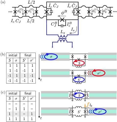
The most basic BSR is the 2-port circuit shown in Fig. 1(a). It consists of a storage cell, one LJJ each for input and output, and a special interface cell between them. The LJJs form a part of the gate and also serve as fluxon in- and output channels. The side arms of the interface cell are formed by two JJs with parameters . Each of them terminates one of the LJJs and thus they are referred to as ‘termination JJs’. The upper rails of the LJJs are joined by a negligible inductance (on the upper side of the interface cell), while the lower rails are connected by the so-called ‘rail JJ’ (of the interface cell), with parameters . The rail JJ is also part of the storage cell which is closed by a parallel inductor . Given suitable parameters (), the storage cell can store one bit of information in form of a steady circulating current. A clockwise (counterclockwise) circulating current corresponds to a positive (negative) flux orientation (), and rail-JJ phase .
Similar to the 1-bit ballistic RFL gates, the NOT or ID, the interface of the BSR is designed to enable forward-scattering, i.e., starting from a fluxon entering on one LJJ and resulting in a fluxon exiting on the other LJJ. By making the in- and output LJJs sufficiently long () we ensure that the ballistic fluxons can move freely. The ballistic gates require specific parameter values in the interface to achieve the operation. The ballistic scattering involves the temporary breaking of the fluxon at the gate interface and a short oscillation of an interface mode. In previous 1-bit ballistic RFL gates, i.e., the NOT and ID, the polarity of the exiting fluxon is determined by the polarity of the incoming fluxon alone. In contrast, the output bit of the BSR is dependent on the stored bit state . The ballistic scattering dynamics generates the regular operations of a shift register, summarized in the table of Fig. 1(b). One of the four possible operations of the BSR is sketched in Fig. 1(b). In comparison with the operation of the ADF flux shuttle FulDynAnd1973_fluxshuttle ; FulDun1973_expfluxshuttle , Fig. 1(c), it uses no external drive power to advance the stored SFQ from the storage cell. Instead, the incoming bit state is swapped efficiently with the stored one in a reversible process.
We refer to the BSR of Fig. 1(a), where fluxons can arrive on only one input LJJ, as a 1-input BSR, to distinguish it from a BSR with separate write and read channels, cf. Fig. 5. The circuit dynamics of the 1-input BSR is described by the Lagrangian
| (1) | |||||
Herein, are the Lagrangian components of the left and right LJJ, respectively, and describes the interface which connects them. The JJs in the discrete LJJs have capacitance and critical current of , and each unit cell of length has the inductance . The characteristic time, length, speed and energy scales of the LJJ are set by the Josephson plasma frequency , the Josephson penetration depth, , the Swihart velocity , and the energy scale (A static fluxon in the LJJ has energy , cf. Eq. (10)).
In our design the inductance in the interface cell is assumed to be negligible, as indicated in Fig. 1(a), and in this situation the phase of the rail JJ of the interface is not independent but fixed by
| (2) | |||
| (3) |
where we introduce shorthand notations for the termination JJ phases in Eq. (3). With this approximation, the interface Lagrangian corresponding to Fig. 1(a) reads
| (4) |
where the parameter quantifies an external flux applied to the storage cell, cf. Fig. 1(a). A finite may be useful during the initialization of the BSR, i.e. the initial loading of an SFQ into the storage cell, but it is not necessary in principle. During regular BSR operations, an SFQ is already stored and is set to zero. In this work we present results on: regular BSR operations (where ) and initialization results using .
II.2 Steady states of the circuit (before input)
To analyze the bit-storage characteristics of the BSR we first study the steady states of the BSR circuit (in the absence of a moving fluxon). It is helpful to first compare the BSR to the earlier ballistic gate circuit without a storage cell. Schematically, in the limit of infinite storage cell inductance the BSR circuit is equivalent to the circuit of the ID and NOT gates WusOsb2020_RFL . The steady states of Eq. (1) are then given by uniform phase fields in the left and right LJJ, and (), while the rail phase assumes the value . Herein, the integers label the ‘vacuum’ states (ground states) of the -periodic LJJ potential Rajaraman . Similar to uncoupled LJJs, all configurations are degenerate here, and the dynamics are not dependent on their initial values. When a fluxon from the left LJJ is scattered forward without (with) polarity inversion it realizes an ID (NOT) gate; it transfers the system from a state with to the state with . By the way, the dynamics of the NOT gate, but not the ID gate, will be used below for the BSR.
In the presence of finite in the BSR the degeneracy of different configurations is lifted due to the contribution in the potential, cf. Eq. (II.1). Large values of the rail phase (and of the vacuum level difference to the left and right of the interface) become energetically inaccessible. At finite , while the LJJ phases far away from the interface are still confined to their respective vacuum levels , the LJJ phases near the interface are perturbed. We therefore model the LJJ phases (in the absence of a fluxon) as bound states with evanescent fields of the form
| (5) | |||||
where is the inverse decay length. Assuming that the bound-state amplitudes are small, the corresponding rail-phase, , is approximated by the vacuum level difference, . The flux state in the storage cell is determined by the difference in configuration at the left and right side of the interface, .
Inserting Eq. (5) in the Lagrangian (1), the potential can be expressed, in the limit of small bound-state amplitudes, as
| (6) |
Referenced from the interface, each LJJ contribution is reduced to an effective JJ and an effective inductance,
| (7) | |||||
| (8) |
where both are in parallel with the corresponding termination JJ (). In these expressions the inverse decay length of the bound state is not yet determined. However, we can estimate from the condition that the bound state fulfills the dispersion relation in the LJJ bulk, . Being interested in steady states of the interface, we can set and obtain the estimate .
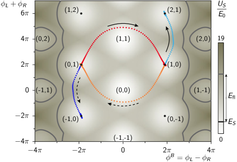
The potential shown in Fig. 2 is obtained from Eq. (II.2) by choosing the energy-minimizing configuration, , for each point . The resulting diamond-shaped domains are labeled in Fig. 2 by the locally minimizing . The potential is -periodic in the sum of the phases at constant phase difference , due to the combined -periodicity in the two components. However, the potential has an approximate parabolic dependence on . For not too large , the potential has a local minimum in each of the domains , and these steady states correspond to a stored flux state . Degenerate global minima are found at in the domains with zero stored flux, . States with a single stored flux quantum are found in the domains with , with the local minima at . From the vertical position of the minima, , it follows that the bound-state amplitudes on the left and right sides of the interface are equal and opposite, .
During normal operation of the BSR, the parameters satisfy , , and , where the bound-state amplitudes are small and the phase fields in the left and right LJJ are nearly uniform. For a single stored flux quantum in the BSR, we can thus approximate in Eq. (5) as . From Eq. (5) it follows that the stored energy relative to the empty BSR () is
| (9) |
If the BSR is initialized with , an incoming fluxon with velocity and energy
| (10) |
can transfer the BSR into a new stored flux state with energy . The equipotential lines in Fig. 2 indicate the corresponding -range accessible from . Energetically, it is not possible to load a 2nd SFQ () into the storage cell, whereas transitions to other states with or are energetically possible.
II.3 Fluxon scattering dynamics
Figure 3 illustrates the BSR operation, where each of the four subfigures shows the circuit simulations for two consecutive input fluxons. In all four cases, the BSR is assumed to initially contain a stored flux quantum . This means that the circuit is initialized in a bound state of the form of Eq. (5), with and corresponding steady state values of . The incoming fluxon(s) are treated in simulation as additional contributions to the initial phase and voltage distribution in the left LJJ, far away from the interface. An input fluxon (antifluxon), which has positive (negative) polarity , is parametrized by the ideal phase distribution with velocity and width . This corresponds to a positive (negative) voltage pulse with maximum (minimum) . We compute the fluxon dynamics from numerical integration of the classical circuit equations of motion for the JJs in the LJJs, together with the termination and rail JJs of the interface. The left panels of Fig. 3 show the resulting JJ-voltages at positions () in the left and right LJJ. The position of the interface is . The right panels of Fig. 3 show the evolution of the rail phase from the initial value .
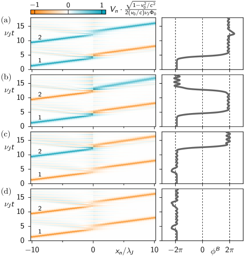
Figure 3(a) shows at the earliest times, a first fluxon with polarity traveling in the left LJJ with nearly constant speed . As it reaches the interface, the fluxon breaks into two parts, i.e. its phase- and voltage-fields become discontinuous. In the process, the energy of the fluxon is coherently transferred to a localized excitation involving the left and right LJJs in form of time-dependent evanescent fields. The localized excitation lasts long enough for its own brief oscillation, and afterwards generates a large field profile in the right LJJ, which eventually moves as a free fluxon in the right LJJ, away from the influence of the interface. During the whole process, the phase of the rail JJ changes monotonously from to . This -phase change indicates the simultaneous transfer of the input fluxon’s (positive) SFQ-state into the storage cell and of the initially stored (negative) SFQ out of the storage cell. Thusly after the scattering, the new orientation of the stored flux quantum is , and the output fluxon carries the negative SFQ-state, , as indicated by the negative sign of the voltage peak. The fluxon scattering dynamics in this case are similar to that of the fundamental (1-bit) NOT gate WusOsb2020_RFL (without a storage cell).
When the second input fluxon with arrives (Fig. 3(a), ), the input SFQ state now equals the stored SFQ state, . The resulting scattering dynamics at the interface therefore differs significantly from that of the preceding fluxon. The interface here acts mostly as a low potential barrier by which the fluxon is slowed down temporarily while retaining its fluxon identity, with unchanged polarity. During the fluxon transmission the rail JJ is only weakly excited away from , indicating that no significant flux transfer occurs. Accordingly, both the fluxon’s state and the stored flux state are unchanged in this process. While the result of the fluxon scattering is here the same as in the fundamental ballistic ID gate (the polarity of the outgoing fluxon is identical to that of the incoming one), the scattering dynamics is different: the fluxon here retains its topological identity throughout the process, whereas in the fundamental ID gate it breaks up into two partial fluxons at the interface and generates a large localized oscillation as a result (which has a longer duration compared with the temporary oscillation in the fundamental NOT gate). The difference of the transmission-type dynamics of the BSR compared with the dynamics of an actual ID-gate originates from the added term in the interface potential, Eq. (II.1). It limits the -range accessible with the fluxon’s initial energy (see Fig. 2 and discussion in Sec. II.2). As a result, the rail phase in the BSR cannot increase from an initial value by . The transmission-type dynamics creates an advantage for the margins of the BSR (see Sec. II.6) relative to the fundamental ID gate, which has somewhat sensitive margins in comparison with the fundamental NOT gate due to the longer resonant oscillation. In summary, the inductor enables bit storage, changes the dynamics relative to previous RFL gates, and improves operation margins compared to an earlier gate.
Figure 3 demonstrates that the scattering dynamics results for all state pairs () in a new state pair, which is related to the old one in the form of a SWAP-operation, () = SWAP(). The ballistic scattering dynamics in the BSR circuit thus generates the state map of a 1-bit shift register, Fig. 1(b). As described above, two different types of scattering dynamics are involved, and in both types the SWAP happens with almost ideal efficiency (cf. Sec. II.6).
The BSR operations can be illustrated as inter-well transitions in the circuit potential , induced by the incoming fluxon. This is illustrated in Fig. 2 by the trajectories (data points), where are taken from the full circuit simulation. Note that the circuit potential shown in Fig. 2 assumes the LJJ fields have the form of a bound state, Eq. (5), but does not take into account the fluxon. For example, a fluxon with leads to a transition (red) from the initial state in the well with to the well with , and this changes the stored flux state . In contrast, a fluxon with induces an -preserving transition (blue), namely to the well with , which is fully equivalent to the initial well. The underlying circuit dynamics for these two processes corresponds to the first fluxon scattering in Figs. 3(a) and (c), respectively. Equivalent dynamics are observed for an initial stored flux state , e.g. initially , if the polarity of the incoming fluxon is inverted at the same time. Thus, an incoming fluxon with () induces a transition that inverts (preserves) , as shown by the orange (light blue) trajectories.
The dynamics shown in Fig. 3 illustrate the regular BSR operations, where initially a flux quantum is already stored in the storage cell. Without this initialization, the BSR will not perform all the intended reversible operations. To initialize a BSR, an SFQ can be loaded into the empty storage cell by sending in a fluxon on the bit line. As the interface cell is designed with minimal inductance, it cannot hold an SFQ. Therefore, once the fluxon is stopped near the interface, its flux is transferred into the storage cell. We find that it is possible to load the BSR in this way with an SFQ, using no external flux () and a fluxon of nominal energy . A lower-energy fluxon () might be better for loading because less excess energy would have to dissipate prior to reaching a quiescent state, but due to a potential barrier a very slow fluxon reflects from the interface instead of trapping. We found that the potential barrier can be lowered by applying an external flux (), and in that case a low energy fluxon () is successfully loaded into the storage cell.
The above initialization procedure seems suitable for individual BSRs. Another procedure may be favorable in a large circuit with many BSR gates. A suitably designed circuit could in principle be made to trap flux solely in the BSR storage cells. To initialize many BSR gates in such a circuit one would cool through the superconducting transition in a magnetic field, and then turn off the field.
II.4 Sequentially arranged shift registers
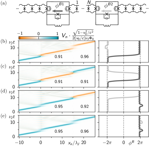
A multi-bit shift register can be constructed from sequentially arranged BSRs, constituting a Serial-In-Serial-Out (SISO) register. As an example, Fig. 4 shows a 2-bit serial shift register and its dynamics. The two bits are stored in one of four different configurations , , , and . Subfigures 4(b-e) show the gate dynamics for each of these initial configurations and a single input fluxon, here with . The two BSR are located at and (separated by LJJ cells). As in Fig. 3, the stored flux quanta can be inferred from the values of the rail-JJ phases and in the right panels of each subfigure, using that (). The operation of the entire 2-bit shift register is powered by the energy of the input fluxon, which looses only a fraction of its kinetic energy in each of the scatterings. The numbers printed in the left panels are the output-to-input velocity ratios after each scattering, and , where again we use initial velocity , corresponding to an initial energy of . The lowest velocity ratio () corresponds to energy conservation according to Eq. (10).
For each scattering type (NOT and transmission), both stages of the 2-bit shift register give approximately the same velocity ratios ( for NOT, for transmission), corresponding to those of a 1-bit BSR (see Sec. II.6). The observed small variability in forward-scattering efficiency at the 1st and 2nd BSR (e.g. between 0.95 and 0.96 for the two consecutive transmissions in panel (e)) can be attributed to the presence of fluctuations in the connecting LJJ and at the 2nd BSR prior to the fluxon arrival there. These fluctuations are emitted from the first BSR during the first scattering event.
Due to a relatively sharp lower cut-off velocity of the transmission dynamics of one BSR, cf. Fig. 6(f), we believe that may be the maximum number of sequentially arranged BSRs for a realistic circuit design without added power. It is beyond the scope of the paper to discuss how to reach a -bit sequential shift register with larger , but we plan to address this in future work.
II.5 2-input shift register
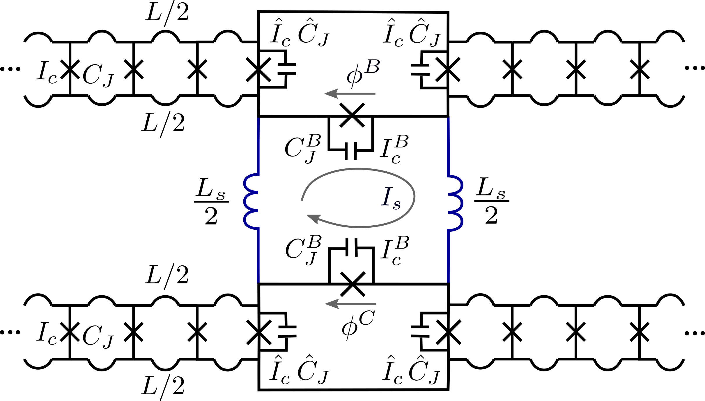
The 1-bit BSR, shown in Fig 1(a), has one input LJJ and one output LJJ. Together they form a single channel called a bit line for the forward-scattering fluxon. This 1-input 1-bit BSR may be generalized to a 2-input 1-bit BSR, where a storage cell is shared between two such scattering channels, as shown in Fig. 5. We have verified in simulations that the 2-input structure also acts as an energy-efficient 1-bit BSR, using the same interface parameters as for the 1-input 1-bit BSR, cf. Table 1. For the operation of this BSR, it is irrelevant which of the two input LJJs a fluxon is sent in on – the dynamics for both input cases is equivalent and it is qualitatively equivalent to the dynamics of the 1-input BSR. In the 2-input device the role of the rail-JJ phase of the 1-input BSR is taken over by the phase difference of the two rail JJs, . Motivated by the small difference in parameter margins between the 1-input and the 2-input version of the BSR, cf. Table 1, we expect that a version with many inputs would also operate. This implies that a stored bit of information could be routed to one of many outputs.
Despite the shared storage cell there is no strong dynamic coupling between the upper and lower part of the gate. By that we mean that even during the NOT-type scattering an input fluxon on the upper (lower) LJJ induces a large phase change of only in the adjacent (), and a relatively small temporary excitation in (), resulting in an output fluxon only on the upper (lower) output LJJ. A similar observation holds for the transmission-type scattering, however in this case no significant phase change takes place even in the adjacent rail JJ. With this property, the 2-input BSR may be used as an SFQ memory with separate write and read lines.
II.6 Margins

| parameter | 1-input BSR | 2-input BSR | |||||
| 7.5 | -31% | +61% | 92% | -35% | +56% | 91% | |
| 5.4 | -39% | +68% | 107% | -37% | +79% | 116% | |
| 4.7 | -29% | +18% | 47% | -30% | +16% | 46% | |
| 1.6 | -90% | +16% | 106% | -78% | +20% | 98% | |
| 20 | -37% | +130% | 167% | -35% | +124% | 159% | |
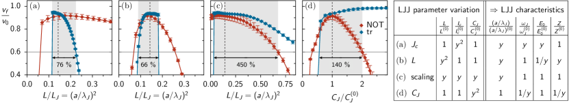
An optimal set of circuit parameters for an energy-efficient BSR are given by the first and second columns in Table 1. These parameters optimize the elastic nature of both scattering types (NOT and transmission) of the BSR operation, such that the dominant fraction of the input fluxon’s energy is conserved in the forward-scattered fluxon. The resulting output-to-input velocity ratio of the optimized dynamics amounts to and , respectively. For an input fluxon with the average energy efficiency of the BSR therefore is 96% according to Eq. (10). Figure 6 shows the output-to-input velocity ratio under variations of different parameters. Setting the minimum ratio to (corresponding to an energy efficiency for initial ), we find the operation margins for the BSR, as shown in the next three columns in Table 1. The current limiting factor of the BSR design, as shown in Fig. 6(f), is the somewhat restricted range of input velocities for the transmission-type BSR dynamics. In this case, the interface’s potential barriers which are proportional to and impose a sharp lower operation limit of , though other parameters can be used to reduce this lower velocity limit. Of the parameter margins, is the smallest with a range of .
In addition to the variation of interface parameters presented in Fig. 6, we have studied gate robustness under variation of LJJ parameters. The resulting margins are generally favourable too, with the smallest range of appearing under variations of the LJJ cell inductances , as shown in Appendix A.
The margins of the 2-input BSR, shown in the last three columns of Table 1, are almost the same as those of the 1-input BSR. This is consistent with our observation earlier, that the dynamics on each (upper or lower) bit line is only very weakly affected by the presence of the other bit line. As long as there is no excitation on the extra bit line, it mainly acts as an inductance added to the storage loop. Therefore, we expect that a BSR gate with more bit lines (an k-input BSR) will operate similarly well.
II.7 Asynchronous gate timing

In most SFQ logic, including RSFQ and its descendants, the gates are clocked, and the SFQ data bit is processed in gates once the clock pulse arrives. Although data bits do not need to arrive at a precise time, the gates are still considered synchronous because the data SFQs must be processed with a clock pulse.
In asynchronous reversible logic gates, the requirements on the arrival time are reduced: operations are not clocked, and bits only need to arrive in a definite order. To achieve definite order, the input constraint is a negligible direct interaction between successive input bits. In the LJJ the interaction strength decays exponentially for large distances compared to Rubinstein1977 , and in our LJJs we find that is a suitable distance for negligible interactions. For an asynchronous 1-input gate like the 1-bit BSR, this corresponds to a minimum required delay time between two input fluxons, , where is the (common) input velocity and is the maximum duration of all possible gate operations. To explore the role of the delay time , this section investigates (i) the dependence of the BSR on and (ii) vice versa, i.e. the modification of the fluxon delay after the BSR gate. Finally, the gate-induced timing uncertainty is compared with that arising from fluxon jitter.
Next we describe uncertainties created by variation of the fluxon delay time and different gate operations. In the underlying simulations we study a 1-bit BSR initialized with and two consecutive input fluxons with a delay time between them. The initialized gate is in a steady state, but the first gate operation leaves residual energy at the interface. Thus the efficiency of the second operation will depend not only on its own dynamics (operation type), but also that of the preceding one. As a result, each of the four input combinations generate distinct curves (different colors) for the output velocity of the second fluxon, as shown in Fig. 7. These curves exhibit oscillations in with approximate periodicity of , due to the constructive or destructive interaction of the input fluxon with the oscillations remaining from the preceding gate operation. While panel (a) shows the situation in absence of damping, in panels (b,c) we show the results for damping added to the three interface JJs. These JJs are shunted by external capacitances already, unlike those in the LJJ. As an example of some damping we test a case where one has a lossy dielectric in the capacitor such that the effective loss tangent of the JJ and shunt capacitor together are . For reference, this corresponds to parallel resistances of and , in parallel to the shunt capacitors and in Fig. 1(a). Here we choose the LJJ frequency as the reference for the loss tangent because the interface elements temporarily oscillate with approximately that frequency during the gate operation. The added damping in panel (b) give rise to slightly increased -variations and slightly reduce the average relative to the undamped case (panel (a)). We believe these differences are caused because the BSR parameters were optimized in the absence of damping. However the same damping after longer times, as shown in panel (c), diminishes -variations, because the residual gate energy has been reduced significantly over time. In addition, this reduces the -variations between operation types. This shows that the output velocities of gates can be constrained to a range using damping and a specified minimum delay time, regardless of the number of previous gate operations.
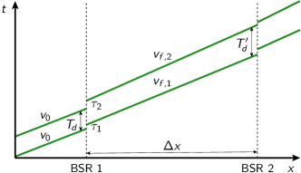
Variability of the gate output velocities and the operation-dependent gate durations gives rise to timing uncertainties for the fluxon arrival at a later gate. Take for example the 2-bit SISO register of Fig. 4(a), where we now consider two input fluxons arriving at the first BSR with an initial delay time between them, as sketched in Fig. 8. After two bits have passed through the first BSR of the SISO, the delay time is in general modified, due to different duration () of the two operations at that BSR. The fluxon delay time also changes during their subsequent motion from the first to the second BSR, due to the different exit velocities () from the first BSR. The final fluxon delay time therefore is , where is the length of the LJJ section between the two BSR gates. Here the and depend on operation type and on . We estimate the final delay time from the simulations of two fluxons given in Fig. 7(c). The figure shows the output velocity of the second fluxon, . The output velocity of the first fluxon is only operation-dependent, and for NOT- and transmission-type, respectively, and is shown as a label in Fig. 4(b-e). We also obtain from the simulations (not shown). From the different input combinations and samples we determine the mean and the maximum of the delay time changes as functions of . Averaging over all input combinations, the delay time remains unchanged from one BSR to the next: , where is the nominal passage time in the connecting LJJ and we assume . However, we find that the dominant delay-time change is caused by different input combinations. The maximum change in delay time is , which comes from the input combination . The maximum negative change in delay time is , which comes from the input combination . For the other two combinations the delay-time changes are comparably small.
As mentioned above, asynchronous gates require a minimum delay time between bits to ensure their interactions are negligible. Since the delay time after the gate can decrease as function of the LJJ length (due to one operation type dominantly) the LJJ should not be too long to still meet the minimum delay criterion. We estimate an upper limit of in the following way: The initial delay time will likely be a factor of the minimum delay time . After the gate operation, the final delay time may be decreased to . Since has to be fulfilled, one obtains the upper limit for the LJJ length of . As a lower limit for the gate-connecting LJJ length we set , i.e. the same value that also ensures negligible fluxon-fluxon interactions. In our experience, LJJs shorter than that can hinder the free fluxon motion between gates.
Another source of timing error is jitter from the LJJs, which is the fluctuation of fluxon passage times caused by thermal noise during its motion in the LJJ. In the ballistic regime of underdamped LJJs, where , the jitter error (standard deviation of arrival times/time) is expected to be small FedorovETAL2007 ; PanGorKuz2012 . Herein, is the damping coefficient of the Sine-Gordon equation ScoChuRei1976 and is given by the loss tangent of the LJJ, , with conductance and capacitance per unit length. In our discrete LJJs, this corresponds to the loss tangent of each JJ, . For example, in a discrete Nb-LJJ with energy scale , cf. Sec. IV, a JJ loss tangent of typical for large-area barriers, and fluxon speed , a conservative estimate for the jitter errorFedorovETAL2007 amounts to for motion over , corresponding to cells of our discrete LJJ. A more refined model PanGorKuz2012 predicts even smaller jitter error. The jitter error for the relevant LJJ lengths is thus expected to be much smaller than the above-estimated timing uncertainty arising from the gate operation. We expect thermal noise in the gate interface itself will also create jitter of the same order of magnitude as the LJJs. Therefore we did not simulate thermal noise in this work.
III Collective coordinate analysis
For solitons and other collective excitations of a many-body system, the collective coordinate (CC) method is a powerful way to reduce the many degrees of freedom to a few essential coordinates Rajaraman . We have previously developed such a CC model for the fundamental (1-bit) RFL gates WusOsb2020_RFL . Here we extend the model to the BSR, in particular the 1-input BSR of Fig. 1. To this end we parametrize the LJJ fields left and right of the interface (at ) with the ansatz
| (11) |
Each (left and right) field consists of a linear superposition of a fluxon and its mirror antifluxon, where is the phase field of a fluxon of polarity which we model as a kink equivalent to the soliton solution of the LJJ field Rajaraman , . Herein, the time-dependent fluxon positions serve as the dynamical coordinates of the model, while the fluxon width is taken to be constant in a so-called adiabatic approximation DauxoisPeyrard . As in Sec. II.2 the integers describe the vacuum levels of the left and right phase fields before the arrival of the fluxon. The resulting rail-JJ phase corresponds to an initial orientation of the stored flux quantum. In comparison, the CC model developed for 1-bit RFL gates WusOsb2020_RFL is based on Eq. (11) with the special case .
The ansatz (11) neglects that for the LJJ fields may deviate in the vicinity of the interface from the vacuum levels, as modelled by the bound states, Eq. (5). However, considering the relatively small bound-state amplitudes of the BSR with , this approximation seems justified.
III.1 CC Model Parametrization and Potential
Examples for the parametrization of Eq. (11) are shown in the insets of Fig. 9 for different points in coordinate space . Subfigures (a-c) represent the different configurations , , and , respectively, for fluxon polarity . A fluxon () initially situated in the left LJJ far away from the interface at , is approximated by Eq. (11) with the coordinate , while describes the absence of excitations in the right LJJ (see left-most inset in all panels (a-c)). For this initial state, Eq. (11) forms a step at the interface () between to the left and to the right, corresponding to the initially stored flux state . With and set by the initial state, Eq. (11) fulfills the boundary conditions, and , for any finite . Under these boundary conditions, four different asymptotic single-fluxon states are permitted and these can be parametrized through suitable choice of : a fluxon (antifluxon) in the left LJJ is parametrized by () together with and a fluxon (antifluxon) in the right LJJ is parametrized by together with (). In the center of the coordinate space, , the phase distribution forms a step between to the left and to the right of the interface, where . At points near , the step is modified by the possible excitations near the interface, see e.g. the inset in bottom right corner of Fig. 9(c). In the corners of the configuration space where , Eq. (11) describes unavailable (high-energy) two-fluxon states (not shown).
Using Eq. (11) we can derive the collective coordinate model for the BSR. This derivation is discussed in detail in Appendix A, while here we simply summarize the results. After inserting Eq. (11) into the system Lagrangian, Eq. (1) is simplified to
| (12) |
where is the dimensionless CC potential, and the mass matrix is composed of the coordinate-dependent, dimensionless elements and (). The CC potential , masses and mass coupling are given in Eqs. (25), (23) and (24), respectively. Compared with the CC model of the 1-bit RFL gates WusOsb2020_RFL , an additional term
| (13) | |||
contributes to the CC potential , cf. Eq. (25), which stems from the shunt current through the inductor .
The diagonal elements of the mass matrix vary with near the interface, but asymptotically () approach a constant value, . The mass coupling is exponentially suppressed far away from the interface, but is finite near it. It is proportional to the rail-JJ capacitance , and this explains the important role of for the forward-scattering of a fluxon from one LJJ to another in many gates. In the fundamental (NOT and ID) RFL gates, mass coupling is the dominant coupling mechanism between the LJJs, whereas coupling generated by the potential is negligible since the potential gradient always acts perpendicular to the coordinate axes, . Relative to the fundmental RFL gates, the BSR has an added contribution in the CC potential which can generate a much stronger coupling between and , depending on the configuration .
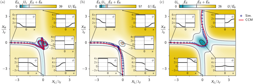
The CC potential is shown in Fig. 9 for the BSR parameters of table 1, , and three different configurations . We emphasize that depends parametrically on parameters of the initial state, namely on the initially stored SFQ, , and on the polarity of the incoming fluxon. Specifically, the dependence enters in form of the product , as can be seen from Eq. (13) for the case of zero external flux through the storage cell, . All other contributions to the CC potential, , , and in Eq. (25), are independent of both and . Note that the product preserves the circuit’s invariance under phase-inversion ( and ), which would only be broken in presence of finite .
Most contributions to the CC potential, , , and in Eq. (25), have mirror symmetry about the line , whereas has this symmetry only for , as can be seen from Eq. (13) for . In Fig. 9 the mirror symmetry is thus seen only in panel (c), where , while in the other cases it is broken. The asymmetry is particularly strong for , panel (b).
A fluxon initially at position , moving with velocity , is parametrized by , , and the related fluxon width . For these initial conditions, the initial energy of the system is found from Eq. (12) to be . Herein, is the initial fluxon energy, Eq. (10), and is the energy of the initially stored flux quantum , as given in Eq. (9). The coordinate space accessible during free evolution with energy is indicated by the corresponding equipotential lines (gray) in Figs. 9(a-c). In Fig. 9(c) this space consists of a central well which connects four asymptotic ‘scattering valleys’. All of these correspond to a single fluxon, but differ by its polarity or its position in either the left or right LJJ, cf. description above. In Figs. 9(a,b), only two of these valleys are connected as a result of the potential’s asymmetry, namely the fluxon’s input valley (, ), with the valley (, ) that corresponds to a forward-scattered fluxon.
The Lagrangian, Eq. (12), generates the coupled equations of motion,
| (18) |
which describe the free dynamics of the coordinates for fixed initial values of and . Recall that in our CC model, Eq. (11), and are mere parameters determined by the initial state. However, as will become clearer in the discussion below, the corresponding values and after the scattering can also be deduced from the asymptotic states of the evolution.
III.2 CC Model Results
From Eq. (18) we obtain the CC trajectories shown in Figs. 9(a-c) (red lines). We also compare the CC trajectories with ‘simulated’ trajectories which are obtained by fitting the phases of the full circuit simulations to Eq. (11) (blue markers). As Fig. 9 demonstrates, there is generally very good qualitative and quantitative agreement with the CC model trajectory.
Next we describe how an empty BSR circuit is loaded with an SFQ such that it is initialized for regular BSR operation. In Fig. 9(a) the trajectory of the incoming fluxon enters the central potential well where it bounces multiple times. Since no damping has been included in the CC dynamics, Eq. (18), the trajectory may eventually exit the well, corresponding to a fluxon emitted from the interface into the left or right LJJ (insets). In the circuit simulations, however, even though no resistances are included, the generation of plasma waves at the interface effectively constitutes a weak damping mechanism which prevents later escape from the interface. For the coordinates trapped near the center point , the phase distribution is close to a step profile (inset pointing to center of coordinate space), whereas the initial fluxon profile has vanished. From a comparison with the initial state (inset pointing to left side of coordinate space), where no flux was stored in the BSR (), it is clear that a flux quantum has now been added to the storage cell, i.e., . While Fig. 9(a) shows the dynamics for a high-energy fluxon () in absence of an external flux through the storage cell, the noise in the loading process can in principle be lowered by using a low-energy fluxon. This decreases the amount of energy that must be lost to capture the fluxon. To avoid back reflection of the low-energy fluxon from the gate interface, one must lower the interface potential by applying a flux .
Figure 9(b) shows results for the initial state . Here the central well of is separated by a potential barrier from the input valley. The trajectory is shown to follow along the curved potential into the scattering valley, which corresponds to a fluxon in the right LJJ, while remains unaffected (inset). This process thus corresponds to the transmission of a fluxon without topological change – the initial phase difference of between the left and right LJJ is therefore roughly maintained during the scattering. In comparison, the dynamics of an ID gate is more complicated (as well as longer in duration), strongly relying on mass-coupling forces (cf. Fig. 4(a) in Ref. WusOsb2020_RFL, ).
Figure 9(c) shows results for the BSR initially in the state . Here the CC potential resembles that of a fundamental 1-bit gates (cf. Fig. 4(a) in Ref. WusOsb2020_RFL, ). The resulting CC dynamics is similar to the NOT fundamental gate dynamics (cf. Fig. 7(c1) in Ref. WusOsb2020_RFL, ), and can be explained by the combined effect of the strong mass-coupling (large ) together with the forces from the potential (, ) and the mass-gradients (, ). The resulting state after the scattering corresponds to a forward-scattered antifluxon, while the stored flux has been inverted, (inset).
As these examples show, the CC model – though heavily simplifying the many-JJ circuit to a reduced system with two degrees of freedom – describes the fluxon scattering in the BSR accurately. Furthermore, it is a good tool to interpret and predict fluxon dynamics at circuit interfaces. With the help of the CC model, we were able to understand how the product , which represents the relative polarity of moving and stored bit states, changes the potential landscape. This in turn changes the scattering dynamics, as we described for the three relevant cases (initialization and the two distinct BSR gate operations).
IV Discussion
Shift registers SR_RSFQ ; SR_AQFP ; Yorozu2003 ; VolETAL2013 ; Ishida2016 ; BautistaETAL2022 constitute a class of superconducting memory Brock2001 ; SolETAL2017 intended to provide fast access to small amounts of data. They are usually loaded as serial input and intended as first-in first-out (FIFO) buffers. This is different than RAM, which is a larger memory intended for addressing in a 2D array. In superconducting logic, the currently available RAM Hidaka2006 ; Tolpygo2019 ; HerrHerr2021 typically builds upon vortex-transition memory Tahara1995 ; Enomoto1999 for SFQ-based logic. However, new AQFP sc_memory_QFP , magnetic-superconducting hybrid sc_memory_piJJ , nanowire-based sc_memory_nanowire1 ; sc_memory_nanowire2 , and DRAM sc_memory_DRAM memories can provide sufficient memory for near-term superconducting logic applications.
In the future we intend to describe how to build large shift registers. The 2-bit shift register described above is made from two 1-bit BSRs. It shows that ballistic gates can in principle be executed in a sequence of two without external power with certain defined constraints. The same holds for the 2-input BSRs and furthermore the simulation data indicates that multi-bit line BSRs can be operated with similar performance. This would allow some bit lines to be used for input and others to be used for sending data to the needed outputs. Having a logical depth of two without external power provides a useful feature because almost every gate is currently clocked (and not sequenced) in most SFQ logic. This could also lead to new methods to incorporate memory with logic (cf. Ref. MajorityGateLogic2020, ). In principle, RFL BSRs could allow greater density than shift register that use dual rail encoding Yorozu2003 because RFL already uses an SFQ for both bit states. We finally note that, in principle, a dual-rail RSFQ could produce an output with both rails merged such that it feeds data into a BSR.
The 2-input BSRs in this work (with 2-outputs) can in principle be used to shift information on-demand in two dimensions (vertically and horizontally). In previous work, we also showed how to make a CNOT gate WusOsb2020_CNOT , which can provide XOR operations. In the future, we plan to release gates to do full digital processing. The XOR operation could give the sum operation for either a half or full adder. To realize such an adder, we plan to study a reversible gate that executes the missing multiplication function.
Logic gates generally have different execution times (delays) Sutherland1991 , and in SFQ logic, delays and jitter lead to requirements for clock and bit synchronization DualRailPolonsky ; DualRailJapan ; Sherwood2021 and sometimes bit arbitration TaharaETAL2001 . However, some progress has been made recently in this area with the introduction of a second time-constant within an AND and OR gate to conveniently define a timing window for receiving the SFQ (bit=1 state) Rylov2019 . Additionally, our asynchronous gates provide a positive development for RFL (and any future bipolar-SFQ logic) because the timing requirement basically reduces to a requirement of bit order. In RSFQ, the (unipolar-bit) T flip-flop is comparable in that it uses no clocking and the bits only need to arrive in a particular order.
Superconducting logic can in principle approach thermodynamic reversibility, meaning that there is no lower limit to energy dissipation. In the past this was studied with so-called adiabatic logics parametricquantron1985 ; SemDanAve2003 ; RenSemETAL2009 ; RenSem2011 ; RQFPgate . In these logic types, adiabatic clock waveforms drive the gates such that the circuit state is always close to a potential-energy minimum. In these adiabatically reversible logic types the dissipated energy scales with the inverse of the clock period such that the thermodynamic limit is approached by lowering the clock frequency. Ballistically reversible logic follows an alternative approach. In ballistic superconducting logic, fluxons in LJJs have been chosen as the bit carriers. The gates are powered by the same input fluxons while no external power is applied. Output states with the same energy as the input states are accessible through the free dynamics powered by the fluxon’s energy entering the gate circuit. Near-thermodynamic reversibility relies on successful exiting of the output fluxon state with a practical velocity while only small amounts of energy are lost to other degrees of freedom. BSRs, similar to previous ballistic RFL gates, satisfy these reversible criteria.
When setting the gate energy efficiency to , we obtain the wide parameter margins shown in Table 1. It follows that the energy cost per operation is , where is the energy of the input bit (which is independent of its bit state). For the assumed input velocity of the fluxon this bit energy is , compared with the rest energy of a stationary bit (cf. Eq. (10)). Herein, the energy scale depends on the LJJ fabrication. The BSR can be fabricated from digital foundry materials, such as Nb superconductor with an AlOx barrier, similar to previous RFL gates Liuqi2019 . For example, in an LJJ built with the discreteness used in our simulations, , and with , an energy cost of would result. When experimentally optimized and realized, this could compare favorably with state-of-the-art logic efficiency results (cf. Ref. YoshikawaETAL2013, ). With other materials, one could in principle lower closer to to achieve an even lower energy cost.
Although it is beyond the scope of this work to specify a full architecture for RFL, it is obvious that the BSRs could be tested by a train of fluxons traveling with some interval between them. For example in the simulation data of Fig. 3, the input fluxons arrive with a time interval of for clarity (smaller intervals are possible). The energy cost estimated above from the circuit simulation includes the loss to plasma waves (from the imperfectly reversible undamped gates). At very high Josephson frequencies comparable to the superconducting gap, additional loss due to quasiparticles is expected and would therefore set an upper limit to the Josephson frequency and the resulting operation speed. Assuming circuits are made with a Josephson frequency and the above-mentioned time interval is used between bits, we calculate a real time interval of . From the rate () and the above energy calculation, the maximum power loss per bit (during operations) is estimated as . Our gates allow a combined benefit of asynchronous timing and energy efficiency. With these modest assumptions, the maximum energy delay product (EDP) for the shift register is less than . Clocking will cost energy as well, and will be addressed in future work. However, we note that an EDP on the order of has been modeled in a one-stage clocked RSFQ architecture Sherwood2021 . In the future, we plan to target low EDP in all of our gates, including those that are less efficient non-ballistic gates (see, e.g., Ref. WusOsb2020_CNOT, for a clock-triggered gate).
V Conclusion
Reversible logic may progress digital computing generally because it allows great improvements in computing efficiency at the gate level. In contrast, end-of-the-roadmap CMOS will have orders of magnitude higher energy cost per bit switching. The type of reversible logic gates which we studied here (RFL BSRs) are ballistic. By introducing the asynchronous feature to ballistic gates, as we have done in this work, we expect greater practicality in our reversible logic family (RFL) since the timing requirements are reduced.
The ADF (Anderson, Dynes, and Fulton) flux shuttle provided a pioneering design for a shift register prior to the start of SFQ logic. That logic is thermodynamically irreversible with the bit’s energy dissipated during every logic operation. In contrast to the ADF shuttle, which has bits encoded by SFQ presence, our RFL ballistic gates conditionally invert fluxon polarity, where the fluxon polarity encodes the bit state. In this work, we introduce BSRs (Ballistic Shift Registers) which add the feature of memory to previous ballistic multi-port gates. The BSRs rely only on ballistic scattering dynamics between the input fluxon and stored SFQ. Here the gate dynamics fall into two cases which consist of the resonant NOT case, generally used in RFL, and a simpler transmission case.
We have performed circuit simulations of a 1-input BSR, as well as a shift register composed of two 1-input BSR gates in sequence. In another design we introduced a 2-input BSR which can be used as a register with separate write and read ports or alternatively as a device to shift the bit state between different bit lines. Furthermore, we discuss how this may be helpful for a register-based memory.
Since the ballistic scattering depends on the stored bit state (unlike previous RFL gates), the 1-input and 2-input BSR constitute the first set of asynchronous reversible logic gates appropriate for feed forward computing. The former (1-input) gate is shown to allow the execution of two in sequence without external power. The latter gate allows more bit lines to be added. We discussed how this is related to logical depth and timing requirements.
Most importantly technically, perhaps, is that the BSR has wide parameter margins, where all margins are above when the energy efficiency is set to 86%. This is far above the variation in today’s standard fabrication processes such that BSRs can be tested.
In addition to full circuit simulations, we have modeled the BSR dynamics by a collective coordinate model which reduces the many-JJ degrees of freedom to only two coordinates. With the help of this model, the state-dependent scattering dynamics can be understood from effective potentials in fluxon coordinate space – the BSR scattering potentials are dependent on the initial fluxon and SFQ states.
All SFQ logic types switch in a time equal or greater than the natural oscillation period of the Josephson junctions. Our logic is a fast reversible logic type in that it is designed to switch in only a few Josephson periods, and it has the potential to be faster than adiabatically powered reversible logic which is generally slowed by the adiabatic power source. Consecutive BSR operations are shown to be possible in less than 8 Josephson periods. We do not currently see the need for an adiabatic clock in contrast to other reversible logic families and this helps enable logic at high speed. Thus, we are optimistic that our ballistic logic may enable high-throughput high-efficiency computation with unpowered gate sequences.
Acknowledgments
KDO would like to thank the Herrs, M. Frank, R. Lewis, N. Missert, I. Sutherland, V. Semenov, K. O’Brien, B. Sarabi, C. Richardson, D. Mountain, G. Herrera, and N. Yoshikawa for stimulating scientific discussions. We thank Seeqc (www.seeqc.com) for their professional foundry services which were used to fabricate RFL gates. WW would like to thank the Physics Department at the University of Otago for its hospitality.
Appendix A Collective coordinate analysis
Here we sketch the derivation of a collective coordinate model for the 1-input BSR of Fig. 1(a), leading to the results discussed in Sec. III. The procedure is similar to the collective coordinate analysis for other RFL gates WusOsb2020_RFL .
The starting point is the circuit Lagrangian, Eqs. (1) with the interface contribution, Eq. (II.1). Inserting the mirror fluxon ansatz, Eq. (11), the LJJ contributions become
| (21) | |||||
where (). To obtain these expressions, we have replaced the LJJ sums in by integrals, based on the small discreteness, . We have evaluated all integrals with boundaries and , which corresponds to including the interface’s termination JJs as part of the LJJ. To correct for this, the corresponding energies have to be subtracted in the interface Lagrangian , Eq. (II.1), such that and . After inserting the ansatz Eq. (11) also into , the full system Lagrangian reads
| (22) |
Herein, the interface modifies the dimensionless mass of Eq. (21) and also contributes a mass-coupling term,
| (23) | |||
| (24) |
where the factor describes the local influence of the interface. The dimensionless CC potential of Eq. (21) is also modified,
| (25) |
with the interface contributions to the potential,
| (26) | ||||
| (27) | ||||
| and | ||||
| (28) | ||||
Using and from Eq. (11), the storage-cell contribution can be written as
| (29) |
Appendix B LJJ parameter margins
Similar to the variation of interface parameters in Fig. 6, in Fig. 10 we show the output-to-input velocity ratio under variations of different LJJ parameters: (a) the JJ critical currents , (b) the cell inductances , (c) the cell inductances along with and the JJ capacitances , and (d) . Case (a) corresponds to a variation of the critical current density . Case (c) can geometrically correspond to linearly scaling the inductor length while scaling the JJ area by the same amount (the dependence of the inductance on the inductor width is more complex). The LJJ parameter variations in general give rise to scalings of (i) Josephson penetration depth relative to unit cell length , (ii) JJ frequency , (iii) LJJ energy scale , and (iv) LJJ impedance , as shown in the table of Fig. 10. The first three variations (a-c) entail variations of the relative lattice spacing , and we present the data in the respective panels as functions of . For most LJJ parameter variations, the margins of this quantity are typically around , as e.g. seen here in cases (a,b). An exception is case (c) where all parameters of the LJJ are scaled by the same factor, as indicated in the table. Here the resulting margins of are almost an order of magnitude larger, and we attribute this robustness to the invariance of the fluxon energy . In contrast, in cases (a) and (b) the fluxon energy is lowered relative to its nominal value for decreasing and increasing values of , respectively. This leads to characteristic edges seen in the variation data of the transmission-type scattering (blue markers), appearing when the fluxon’s initial kinetic energy is too low to overcome the potential barrier on the transmission path.
We note that for large discreteness, , the moving fluxon loses energy through excitation of linear plasma modes in the LJJ WusOsb2020_RFL ; BraunKivshar1998 . Because of the resulting strong damping, the output-to-input velocity ratio in panel (c) becomes increasingly ill-defined for (it becomes dependent on the distance of the measurement points from the gate interface).
Panel (d) shows the varied capacitance relative to its nominal value . We note that all of our simulations are performed with as the sole free parameter, and absolute values of , , and are not specified. However, for the Nb-fabrication assumed in the discussion of Sec. IV, the nominal values become , and . Panel (d) shows wider -margins () compared with the inductance margins of panels (a,b). We attribute this increase to the fact that the fluxon energy is not changed here, unlike in cases (a,b), cf. the table in Fig. 10. However, the margins are also smaller than in the case of panel (c). In case (d) we observe that high values of limit the NOT operation (red markers). This is likely due to the lowered LJJ frequency ; the NOT gate is a resonant process that depends on the frequency of the LJJs.
References
- (1) D.S. Holmes, A.L. Ripple, and M.A. Manheimer, Energy-Efficient Superconducting Computing – Power Budgets and Requirements, IEEE Trans. Appl. Supercond. 23, 1701610 (2013).
- (2) I.I. Soloviev, N.V. Klenov, S.V. Bakurskiy, M.Y. Kupriyanov, A.L. Gudkov, and A.S. Sidorenko, Beyond Moore’s technologies: operation principles of a superconductor alternative, Beilstein J. Nanotechnol. 2017, 8, 2689–2710.
- (3) K.K. Likharev, O.A. Mukhanov, and V.K. Semenov Resistive single flux quantum logic for the Josephson-junction technology, in SQUID’ 85, Berlin, Germany, 1985, pp. 1103-1108.
- (4) K.K. Likharev and V.K. Semenov: RSFQ logic/memory family: a new Josephson-junction technology for sub-terahertz-clock-frequency digital systems, IEEE Trans. Appl. Supercond. 1, 3 (1991).
- (5) D.E. Kirichenko, S. Sarwana and A.F. Kirichenko, Zero Static Power Dissipation Biasing of RSFQ Circuits, IEEE Trans. Appl. Supercond. 21, 776 (2011).
- (6) M.H. Volkmann, A. Sahu, C.J. Fourie, and O.A. Mukhanov, Implementation of energy efficient single flux quantum digital circuits with sub-aJ/bit operation, Supercond. Sci. Technol. 26, 015002 (2013).
- (7) M. Tanaka et al., Development of Bit-Serial RSFQ Microprocessors Integrated with Shift-Register-Based Random Access Memories, 15th International Superconductive Electronics Conference (ISEC) (2015).
- (8) Y. Harada, H. Nakane, N. Miyamoto, U. Kawabe, E. Goto, and T. Soma, Basic operations of the quantum flux parametron, IEEE Trans. Magnetics 23, 3801 (1987).
- (9) C.L. Ayala, T. Tanaka, R. Saito, M. Nozoe, N. Takeuchi and N. Yoshikawa, MANA: A Monolithic Adiabatic iNtegration Architecture Microprocessor Using 1.4- Unshunted Superconductor Josephson Junction Devices, IEEE Journal of Solid-State Circuits 56, 1152 (2021).
- (10) Q.P. Herr, A.Y. Herr, O.T. Oberg, and A.G. Ioannidis, Ultra-low-power superconductor logic, J. Appl. Phys. 109, 103903 (2011).
- (11) R. Landauer, Irreversibility and heat generation in the computing process, IBM Journal of Research and Development 5, 183 (1961).
- (12) Appendix 2 of Ref. LikSem1991, .
- (13) T.A. Fulton, R.C. Dynes, and P.W. Anderson, The Flux Shuttle – A Josephson Junction Shift Register Employing Single Flux Quanta, IEEE Proceedings 61 (1973).
- (14) T.A. Fulton, and L.N. Dunkleberger, Experimental flux shuttle, Appl. Phys. Lett. 22, 232 (1973).
- (15) O.A. Mukhanov, S.V. Polonsky, and V.K. Semenov, New elements of the RSFQ Logic Family, IEEE Trans. Magnetics 27, 2435 (1991).
- (16) O.A. Mukhanov, Rapid Single Flux Quantum (RSFQ) Shift Register Family, IEEE Trans. Appl. Supercond. 3, 2578 (1993).
- (17) W. Wustmann and K.D. Osborn, Reversible fluxon logic: Topological particles allow ballistic gates along one-dimensional paths, Phys. Rev. B 101, 0.14516 (2020).
- (18) K.D. Osborn and W. Wustmann, Reversible Fluxon Logic With Optimized CNOT Gate Components, IEEE Trans. Appl. Supercond. 31, 1, (2021).
- (19) K.D. Osborn and W. Wustmann, Ballistic reversible gates matched to bit storage: Plans for an efficient CNOT gate using fluxons, in Reversible Computation. RC 2018. Lecture Notes in Computer Science 11106, 189 (Springer, Cham, 2018).
- (20) K.K. Likharev, S.V. Rylov, and V.K. Semenov, Reversible conveyer computation in array of parametric quantrons, IEEE Trans. Magn. 21, 947 (1985).
- (21) V.K. Semenov, G.V. Danilov, and D.V. Averin, Negative-inductance SQUID as the basic element of reversible Josephson-junction circuits, IEEE Trans. Appl. Supercond. 13, 938 (2003).
- (22) J. Ren, V.K. Semenov, Y.A. Polyakov, D.V. Averin, and J.-S. Tsai, Progress Towards Reversible Computing With nSQUID Arrays, IEEE Trans. Appl. Supercond. 19, 961 (2009);
- (23) J. Ren and V.K. Semenov, Progress With Physically and Logically Reversible Superconducting Digital Circuits, IEEE Trans. Appl. Supercond. 21, 780 (2011).
- (24) N. Takeuchi, Y. Yamanashi, and N. Yoshikawa, Reversible logic gate using adiabatic superconducting devices, Sci. Rep. 4, 6354 (2014).
- (25) M.P. Frank, Asynchronous Ballistic Reversible Computing, 2017 IEEE ICRC conference proceedings (2017).
- (26) M.P. Frank, R.M. Lewis, N.A. Missert, M.D. Henry, M.A. Wolak, and E.P. DeBenedictis, Semi-Automated Design of Functional Elements for a New Approach to Digital Superconducting Electronics, 2019 ISEC conference proceedings (2019).
- (27) L. Yu, W. Wustmann and K.D. Osborn, Experimental designs of ballistic reversible logic gates using fluxons, Proc. IEEE Int. Superconductive Electron. Conf., 1 (2019).
- (28) R. Rajaraman: Solitons and Instantons. An introduction to Solitons and Instantons in Quantum Field Theory (North-Holland, Amsterdam, 1989).
- (29) J. Rubinstein, Sine-Gordon Equation, J. Math. Phys. 11, 258 (1970).
- (30) A. Fedorov, A. Shnirman, G. Schön, and A. Kidiyarova-Shevchenko, Reading out the state of a flux qubit by Josephson transmission line solitons, Phys. Rev. B 75, 224504 (2007).
- (31) A.L. Pankratov, A.V. Gordeeva, and L.S. Kuzmin Drastic Suppression of Noise-Induced Errors in Underdamped Long Josephson Junctions, Phys. Rev. Lett. 109, 087003 (2012).
- (32) A.C. Scott, F.Y.F. Chu, and S.A. Reible, Magnetic-flux propagation on a Josephson transmission line J. Appl. Phys. 47, 3272 (1976).
- (33) T. Dauxois and M. Peyrard, Physics of Solitons (Cambridge University Press, Cambridge, 2006).
- (34) O.A. Mukhanov, RSFQ 1024-bit Shift Register for Acquisition Memory, IEEE Trans. Appl. Supercond. 3, 3102 (1993).
- (35) M. Hosoya, W. Hioe, K. Takagi, and E. Goto, Operation of a 1-bit quantum flux parametron shift register (latch) by 4-phase 36-GHz clock, IEEE Trans. Appl. Supercond. 5, 2831 (1995).
- (36) K. Fujiwara, Y. Yamashiro, N. Yoshikawa, A. Fujimaki, H. Terai, and S. Yorozu, Design and high-speed test of (4 8)-bit single-flux-quantum shift register files, Supercond. Sci. Technol. 16, 1456 (2003).
- (37) K. Ishida, M. Tanaka, T. Ono, and K. Inoue, Single-flux-quantum cache memory architecture, 2016 International SoC Design Conference (ISOCC), 105 (2016).
- (38) M.G. Bautista, P. Gonzalez-Guerrero, D. Lyles, and G. Michelogiannakis, Superconducting Shuttle-Flux Shift Register for Race Logic and Its Applications, IEEE Transactions on Circuits and Systems I: Regular Papers, 1 (2022).
- (39) D.K. Brock, RSFQ TECHNOLOGY: CIRCUITS AND SYSTEMS, International Journal of High Speed Electronics and Systems 11, 307 (2001).
- (40) S. Nagasawa, K. Hinode, T. Satoh, Y. Kitagawa, and M. Hidaka, Design of all-dc-powered high-speed single flux quantum random access memory based on a pipeline structure for memory cell arrays, Supercond. Sci. Technol. 19 S325 (2006).
- (41) V.K. Semenov, Y.A. Polyakov, and S.K. Tolpygo, Very Large Scale Integration of Josephson-Junction-Based Superconductor Random Access Memories, IEEE Trans. Appl. Supercond. 29, 1302809, (2019).
- (42) Q.P. Herr and A.Y. Herr, Superconducting Digital Computing: Promise-Progress-Prospects, Semicon Europa, Munich (2021).
- (43) S. Nagasawa, Y. Hashimoto, H. Numata, and S. Tahara, A 380 ps, 9.5 mW Josephson 4-Kbit RAM operated at a high bit yield, IEEE Trans. Appl. Supercond. 5, 2447 (1995).
- (44) S. Nagasawa, H. Hasegawa, T. Hashimoto, H. Suzuki, K. Miyahara, and Y. Enomoto, Design of a 16 kbit superconducting latching/SFQ hybrid RAM, Supercond. Sci. Technol. 12 933 (1999).
- (45) H. Takayama, N. Takeuchi, Y. Yamanashi, and N. Yoshikawa, A random-access-memory cell based on quantum flux parametron with three control lines J. Phys.: Conf. Ser. 1054, 012063 (2018).
- (46) I.A. Dayton, T. Sage, E.C. Gingrich, M.G. Loving, T.F. Ambrose, N.P. Siwak, S. Keebaugh, C. Kirby, D.L. Miller, A.Y. Herr, Q.P. Herr, O. Naaman, Experimental Demonstration of a Josephson Magnetic Memory Cell With a Programmable -Junction, IEEE Magnetics Letters 9, 3301905 (2018).
- (47) Q.-Y. Zhao, E.A. Toomey, B.A. Butters, A.N. McCaughan, A.E. Dane, S.-W. Nam, and K.K. Berggren, A compact superconducting nanowire memory element operated by nanowire cryotrons, Supercond. Sci. Technol. 31, 035009 (2018).
- (48) A. Murphy, D.V. Averin, and A. Bezryadin, Nanoscale superconducting memory based on the kinetic inductance of asymmetric nanowire loops, New J. Phys. 19, 063015 (2017).
- (49) F. Wang, T. Vogelsang, B. Haukness, and S.C. Magee, DRAM Retention at Cryogenic Temperatures, 2018 IEEE International Memory Workshop (IMW), Kyoto, Japan (2018).
- (50) J. Reuben, Rediscovering Majority Logic in the Post-CMOS Era: A Perspective from In-Memory Computing, J. Low Power Electron. Appl. 10, 28 (2020).
- (51) I.E. Sutherland and R.F. Sproull, Logical Effort: Designing for Speed on the Back of an Envelope, in Proc. of the 1991 University of California/Santa Cruz conference on Advanced research in VLSI (MIT Press, Cambridge, 1991).
- (52) M. Maezawa, I. Kurosawa, M. Aoyagi, H. Nakagawa, Y. Kameda, and T. Nanya, Rapid single-flux-quantum dual-rail logic for asynchronous circuits, IEEE Trans. Appl. Supercond. 7, 2705 (1997).
- (53) P. Patra, S. Polonsky and D.S. Fussell, Delay insensitive logic for RSFQ superconductor technology, Proceedings Third International Symposium on Advanced Research in Asynchronous Circuits and Systems, 42 (1997).
- (54) G. Tzimpragos, J. Volk, A. Wynn, J.E. Smith, T. Sherwood, Superconducting Computing with Alternating Logic Elements, 2021 ACM/IEEE 48th Annual International Symposium on Computer Architecture (ISCA), 651, (2021).
- (55) S. Yorozu, Y. Kameda, S. Tahara, 60 Gbps throughput demonstration of an asynchronous SFQ-pulse arbitration circuit, IEEE Trans. Appl. Supercond. 11, 621 (2001).
- (56) S.V. Rylov, Clockless Dynamic SFQ and Gate With High Input Skew Tolerance, IEEE Trans. Appl. Supercond. 29, 1300805 (2019).
- (57) N. Takeuchi, Y. Yamanashi, N. Yoshikawa, Measurement of energy dissipation of adiabatic quantum-flux-parametron logic using a superconducting resonator, Appl. Phys. Lett. 102, 052602 (2013).
- (58) O.M. Braun and Y.S. Kivshar, Phys. Rep. 306, 1 (1998).