Limitations to Electrical Probing of Spontaneous Polarization in Ferroelectric-Dielectric Heterostructures
Abstract
An accurate estimate of the ferroelectric polarization in ferroelectric-dielectric stacks is important from a materials science perspective, and it is also crucial for the development of ferroelectric based electron devices. This paper revisits the theory and application of the PUND technique in Metal-Ferroelectric-Dielectric-Metal (MFDM) structures by using analytical derivations and numerical simulations. In an MFDM structure the results of the PUND technique may largely differ from the polarization actually switched in the stack, which in turn is different from the remnant polarization of the underlying ferroelectric. The main hindrances that prevent PUND measurements from providing a good estimate of the polarization switching in MFDM stacks are thus discussed. The inspection of the involved physical quantities, not always accessible in experiments, provides a useful insight about the main sources of the errors in the PUND technique, and clarifies the delicate interplay between the depolarization field and the charge injection and trapping in MFDM stacks with a thin dielectric layer.
Index Terms:
HZO, Ferroelectric, MFDM, Dielectric, PUND, Depolarization© 2022 IEEE. Personal use of this material is permitted. Permission from IEEE must be obtained for all other uses, in any current or future media, including reprinting/republishing this material for advertising or promotional purposes, creating new collective works, for resale or redistribution to servers or lists, or reuse of any copyrighted component of this work in other works.
I Introduction
Thanks to the discovery of a robust ferroelectricity in hafnium oxide thin films, several intriguing applications of ferroelectricity in CMOS electron devices have been proposed and are being presently scrutinized. Device concepts include nanoscale CMOS FETs exploitating the effective negative capacitance to improve the subthresholdswing, as well as Ferroelectric Tunnelling Junctions (FTJs), and ferroelectric FETs, which may be used as non–volatile memories or as memristors for neuromorphic computing applications.
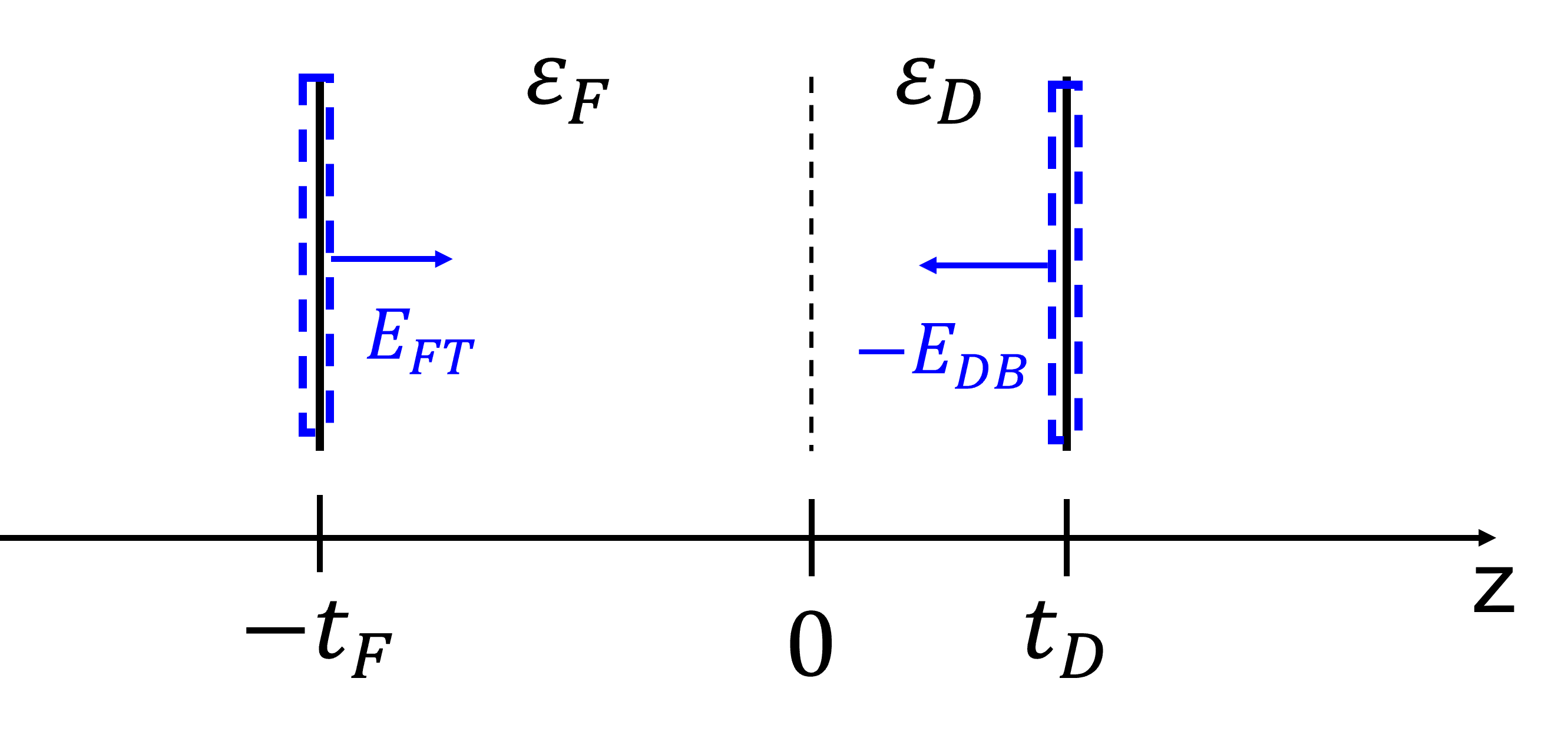
In most of the above material systems and electron devices, one of the materials adjacent to the ferroelectric is a dielectric (see also Figure 1), and the working principle of the devices relies on the influence that the ferroelectric polarization, , exerts on the band bending inside the device. Quite understandably, a dependable determination of is of primary importance in ferroelectric materials and ferroelectric based electron devices. To this purpose the Positive-Up-Negative-Down (PUND) measurement technique was originally conceived for Metal-Ferroelectric-Metal (MFM) structures (see also PUND waveforms in Figure 2), and it is still routinely used also in Metal-Ferroelectric-Dielectric-Metal (MFDM) device structures. The main goal of the PUND technique for an MFM structure is an accurate determination of the difference, 2, between the polarization at zero ferroelectric field for the positive and negative polarization state. In an MFM stack with ideal metal electrodes the field can be zeroed by using a zero external voltage, and the PUND measurements essentially intend to minimize the contributions to 2 due to the background ferroelectric polarization and to possible leakage currents (see also the discussion in Section II). In an MFDM structure, however, a zero external voltage cannot force a zero ferroelectric field due to the depolarization field, and the application of the PUND technique to MFDM devices is not straightforward in several respects. In fact the interpretation of PUND results in an MFDM stack can lead to artifacts and to a misleading information about the polarization of the underlying ferroelectric layer. We here revisit the theory and application of PUND measurements in MFDM structures, and to this purpose we use both analytical derivations and a comprehensive modelling framework, that has been previously validated and calibrated against experiments. Our results show that: a) the determination of the spontaneous ferroelectric polarization is challenging in MFDM structures even if the charge injection and trapping in the dielectric stack is negligible; b) in the presence of a non negligible charge injection and trapping, the variations of spontaneous polarization and trapped charge are inextricably entangled, which further complicates the extraction of the switched polarization; c) the dependence of the extracted polarization can be an artifact due to the ( dependent) interplay between the depolarization field and charge trapping. The paper is organized as follows. In Section II we present the theoretical background behind the extraction of the spontaneous polarization from the terminal currents measured by the PUND technique. In Section III we provide an overview of our in house modelling framework and then in Secs. III-B and III-C we report simulation results about the ability of the PUND technique to determine the switched polarization in MFDM structures, and offer an insight about the main sources of errors. In Section IV we propose a few concluding remarks and in the Appendix provide additional details about some aspects of the modelling framework.
II Charge and current at the electrodes in the MFDM structure
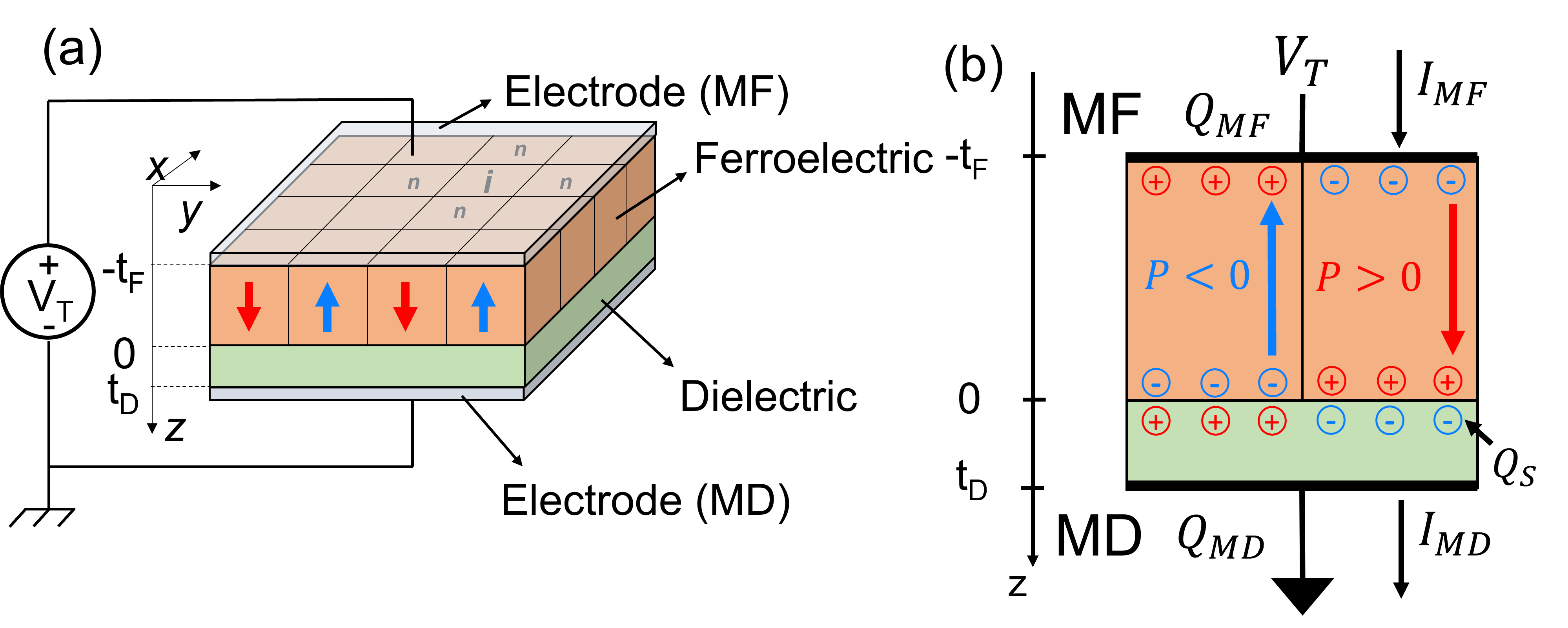
Let us consider the MFDM structure sketched in Figure 1(a), where and are the coordinate in the plane of the ferroelectric-dielectric interface and in the direction normal to the interface, while , are the charges per unit area respectively at the MF and MD electrodes, respectively (see Figure 1). Assuming a perfect screening in the metal electrodes, the electrostatic problem is linear and , can be written by using appropriate Green’s functions for the charges in the structure. More specifically, for we have
| (1) |
where is the device area, is the ferroelectric spontaneous polarization, denotes the component of the electric field at the position r of the MF-FE interface (namely at ).
At any time , the is determined by the external bias and by the charges in the dielectric stack, that are charges located at coordinate defined as r at = 0. In this latter respect, we here define the depolarization field, , at the MF-FE interface as the field produced by the distribution of the total charge + at the FE-DE interface, where is an interface charge due to fixed Coulomb centers or to interface traps. We also similarly introduce as the field produced by the remaining charge densities in the dielectric stack at . The can thus be written as
| (2) |
where , with , and , being the thickness and relative permittivity of the dielectric, and , being the thickness and background permittivity of the ferroelectric (see Figure 1(b)). By substituting Equation 2 in Equation 1 we obtain
| (3) |
where , and denote respectively the average polarization and average fields at the MF-FE interface. From A of the Appendix it can be inferred that the average and can be written as:
| (4a) | |||
| (4b) |
where is the Green’s function defined as
| (5) |
with being the field produced by a point charge located at . In B of Appendix we also demonstrate that, under realistic assumptions, the for the MFDM structure in Figure 1(b) is independent of and it can be evaluated analytically. For a charge located at the FE-DE interface, for example, we have , which allows to rewrite Equation 4a as
| (6) |
At any the can be similarly expressed with a dependent capacitance ratio.
We now recall that PUND measurements are based on the integral of the transient current at the electrodes, hence by definition the experiments can probe only the variations of the polarization and charges in the device stack.
Here below the discussion is carried out in terms of the current at the MF terminal; in B of Appendix we report the corresponding expression for .
In the presence of a trapping distributed throughout the device, it is thus difficult to express the influence of on , because Equation 4b shows that the information about the distribution along is required.
Consequently, hereafter we simplify the picture and assume that the time derivative of the charge trapped in the dielectric stack is dominated by the term due to traps at the FE-DE interface, which implies
. We also assume that can change only through the terminal currents , shown in Figure 3, and we let denote a possible leakage current, not contributing to trapping. The current at the MF electrode can thus be written as
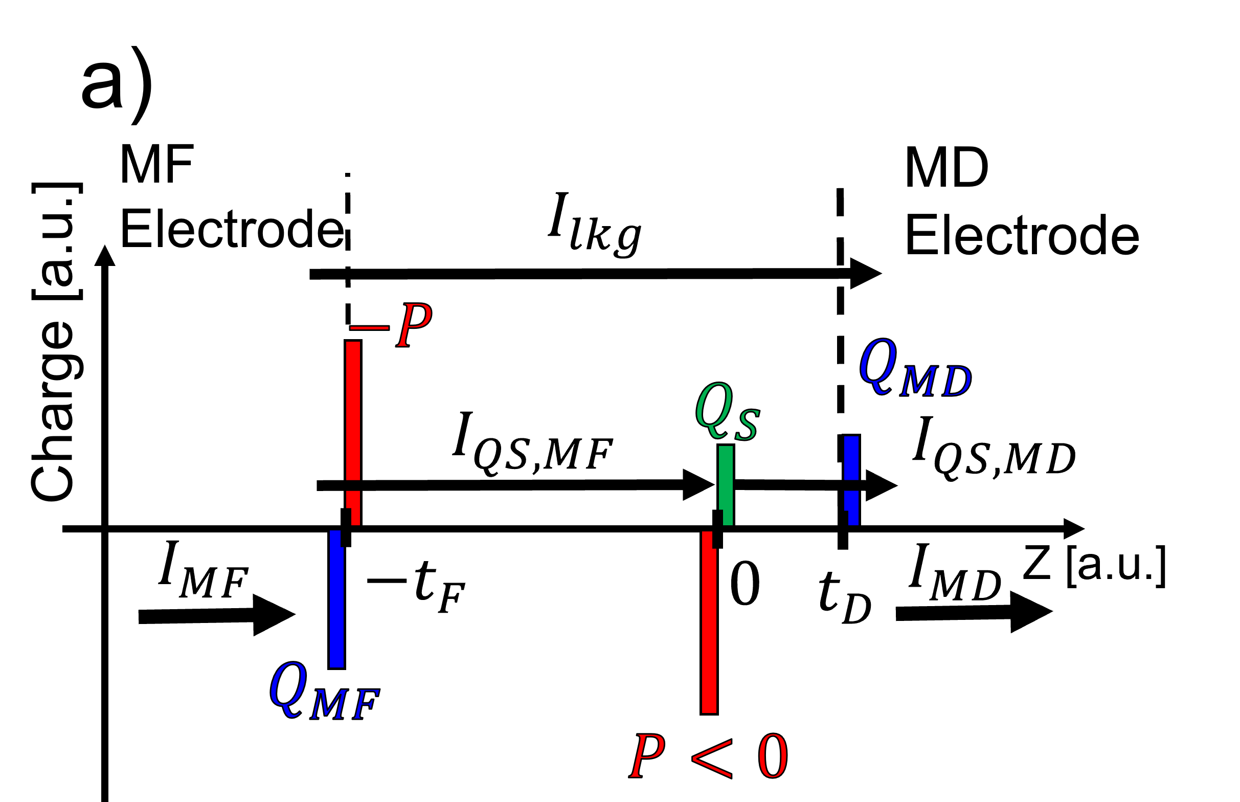
| (7) |
where has been expressed via Equation 3 assuming , and in the last equality we have used Equation 6.
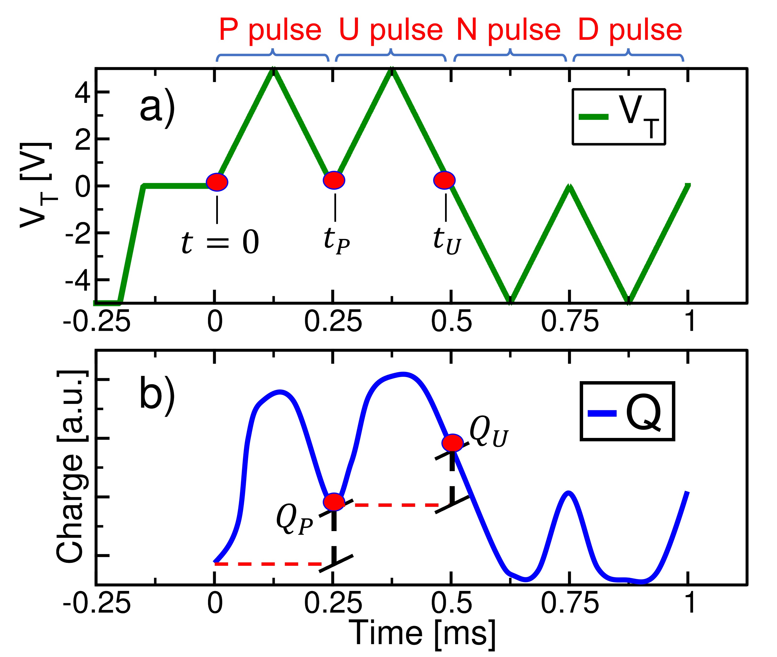
If we now consider the Positive (P) pulse of a PUND experiment starting at = 0 s with = 0 V (see the waveform in Figure 2(a)), we can evaluate the charge (with ) by integrating the expression for in Equation 7 and obtain
| (8) |
where and are the integral of and , respectively. Moreover it is understood that , and in Equation 8 denote the variations from the corresponding values at 0 or, equivalently, that Equation 8 conventionally assumes 0 at 0. The charges , , during respectively the Up (U), Negative (N) and Down (D) pulses of the PUND technique have expressions equivalent to Equation 8.
The first and last term at the right hand side of Equation 8 are the contributions due to, respectively, the linear polarization of the dielectrics and the leakage. Even in an MFM structure these contributions complicate the extraction of the remnant polarization , and PUND measurements address this issue by subtracting from the charge during the U pulse at the same external bias .
In our theoretical framework such an approach results in the charge
, that can be written as
| (9) |
where the apices , identify the P and U pulse and all charges are evaluated at times corresponding to the same value during either a rising or a falling ramp. We recall that, as already mentioned about Equation8, the , and in Equation 9 denote the variations from the corresponding values at the beginning of either the P or the U pulse.
The second and third term in the right hand side of Equation 9 are due respectively to the depolarization field and the current at the MF electrode contributing to trapping at the FE-DE interface. In an MFM structure both these terms are negligible and, moreover, it is typically assumed that the polarization can be stabilized after the P pulse, so that is much smaller than . Furthermore, it is also usually assumed that the leakage affects the measurements to a similar extent during the P and U pulse, leading to . Under these circumstances Equation 9 shows that the in an MFM stack can be interpreted as the that we wish to determine. In an MFDM structure, instead, the terms in Equation 9 due to the depolarization field can be comparable to , and the term may also give a sizeable contribution to . Hence in an MFDM stack the interpretation of and the determination of appear much more delicate that in the MFM counterpart. This is systematically investigated in SectionIII by using numerical simulations.
III Numerical simulations and discussion
The goal of the PUND measurements is to accurately determine the spontaneous polarization switched by the external bias, which is very challenging in an MFDM structure due to the depolarization field and the possible charge trapping. In this section, we use numerical simulations to investigate the possible errors and artifacts produced by PUND measurements in MFDM structures, and to provide some useful physical insights.
III-A Modelling framework and validation
Our in house developed simulation framework comprises models for the ferroelectric dynamics, a dynamic equation for the traps at the FE-DE interface and a description of a tunnelling injection from the MF and MD electrodes to the traps. The dynamics of the ferroelectric domains is described by a formulation of the multi-domain Landau-Ginzburg-Devonshire (LGD) model more thoroughly discussed in
| (10) |
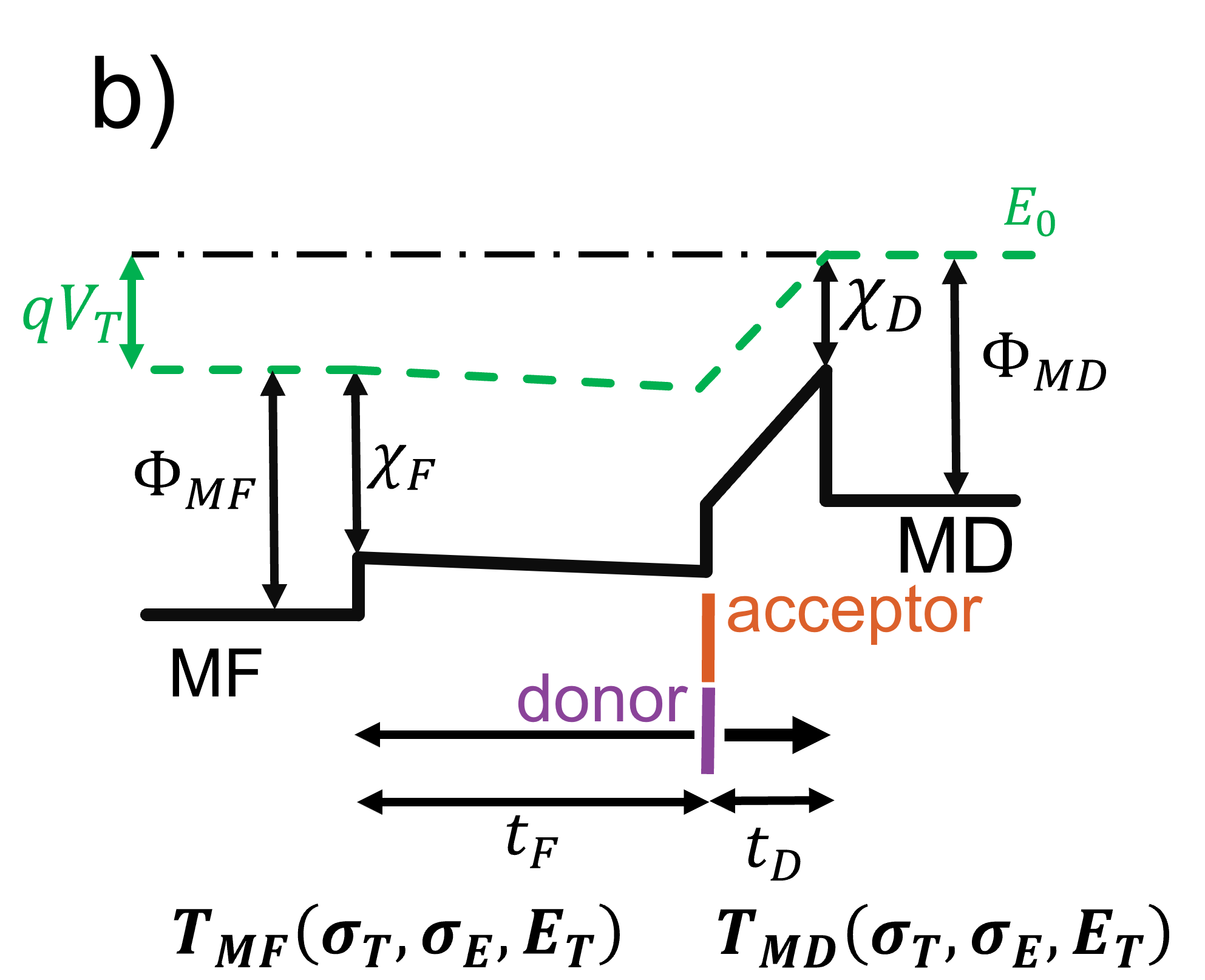
where , , are the anisotropy constants, denotes the resistivity that sets a time scale for the ferroelectric switching. Moreover, the parameters describe the depolarization energy and depolarization field in the MFDM structure, while and are the coupling constant and the domain wall width involved in the formulation of the domain wall energy. The mean values for , , used in simulations are reported in Table I and are referred to Hafnium-Zirconium-Oxide (HZO) ferroelectric which is the current state-of-the art ferrolectric used in FTJs. In all simulations the domain wall coupling was set to zero, by following recent first principles calculations for HfO2. Moreover, we assumed a resistivity 115 m, which is consistent with recently reported values for Hafnium-Zirconium (HZO) based capacitors, and results in a time scale for the ferroelectric dynamics ns. All simulations include a 1024 and a domain size d=5nm; we verified that results are insensitive to a further increase of . The modelling for the ferroelectric dynamics has been extensively compared to transient negative capacitance measurements, demonstrating a good agreement with experiments in asymmetric MFDM dielectric stacks, and also in symmetric MFDFM structures. The charge trapping model follows a first-order dynamic equation for the occupation of either acceptor or donor type traps at the FE-DE interface. By denoting with , the capture rate from the metal MD and MF electrodes the equation governing can be written as
| (11) |
where is the Fermi occupation function in the metal electrodes, with =. In the derivation of Equation 11 we used a detailed balance condition, ensuring that the steady state value at the equilibrium (i.e. for = V) is given by the Fermi function. In this work, the capture rates were attributed to tunnelling from and to the electrodes, and the tunnelling transmission described according to a WKB approximation that involves the tunnelling effective mass in the two dielectrics , , and the area and energy cross sections [m2], [eV] (see also Figure 3). More details about the trapping and tunnelling models may be found in reporting also a good agreement with the polarization versus voltage curves in FTJs with an MFDM structure and a thin dielectric layers. The values of , , , used in this work are reported in Table I.
From the occupations one can readily calculate the charges and respectively in acceptor and donor type traps, and finally the overall interface trapped charge (. The knowledge of the time dependent polarization and trapped charge, in turn, allows one to numerically calculate all the quantities discussed in Section II, such as , , , and also , .
| [m/F] | [m5/C2/F] | [m9/C4/F] | m [m0] | m [m0] | [m2] | [eV] | ||
|---|---|---|---|---|---|---|---|---|
III-B Simulations results
We used numerical simulations to emulate PUND measurements with a 1 kHz waveform and a 5 V peak voltage in an MFDM structure with different dielectric thicknesses and trap densities and . The ferroelectric HZO layer is 10 nm thick in all simulations.
We do not account for a possible leakage current flowing directly from MD to MF. Here we did not attempt to model the leakage current because we think that leakage is strongly technology dependent, frequently governed by Poole-Frenkel and hopping mechanisms in the the HZO and, as such, difficult to describe in simulations. Moreover, while it is understood that a failure of the condition can induce artifacts in PUND experiments even in an MFM stack, this issue goes beyond the scope of the present paper, that is focused on the influence that the depolarization field and charge trapping have on the results of PUND measurements in MFDM structures.
In Figure 4 we report simulation results for 1.5 nm and for different trap densities. The is here defined as either or , respectively for the positive and negative values. The sign of the interface charge is typically opposite to the sign of the polarization, and Figure 4 reports , which together with determines according to Equation 6. All charges in Figure 4 are referred to the corresponding value at the beginning of the P pulse, namely at 0 s and 0 V in Figure 2 (see also the discussion about Equations 8 and 9). The in Figure 4(a) shows a hysteresis loop that is much more tilted and stretched than in the corresponding MFM curves (filled triangles). The features for an MFDM are similar to those experimentally observed in the - curves for an HZO capacitor serially connected to a discrete ceramic capacitor ensuring a negligible charge injection, or to measurements in MFDM structures with thicker Al2O3 layers. In fact, the relatively low density of traps in Figure 4(a) results in an interface charge (green diamonds) that is practically negligible compared to the ferroelectric polarization (red squares). The lack of any compensation of the polarization results in a large depolarization field (see Equation 6), which in turn leads to a vast discrepancy between and . In fact, Figure 4(a) shows that for above about 4 V a complete polarization switching occurs. Nevertheless the corresponding is much smaller than , mainly because the term in Equation 9 subtracts from the term due to the opposite sign. The results for are quite different in Figure 4(b), because the can now compensate to a large extent, thus drastically reducing the depolarization field. The hysteresis loop of the curve in Figure 4(b) is qualitatively similar to the experimental behaviour observed in FTJ structures with a thin tunnel oxide, and the discrepancy between and is much smaller than in Figure 4(a).
Figure 5 illustrates the same analysis as in Figure 4, but for a larger dielectric thickness = nm. In this case the results of both small and large interface traps densities have a qualitative behaviour similar to Figure 4(a), namely the is very small (green diamonds) and the compensation of the ferroelectric polarization is minimal. For both traps densities, the depolarization field results in a much smaller than .

The different behaviour in Figure 5(b) compared to Figure 4(b) is due to the fact that, according to the tunneling effective masses and traps cross-sections reported in Table I, the trapping and de-trapping dynamics cannot follow the 1 kHz waveform for 2.5 nm or larger. In fact, because the HZO layer is 10 nm thick, in the simulations of this work the trapping dynamics is essentially set by the tunnelling through the much thinner dielectric layer. The lack of modulation in Figure 5(b) is thus a dynamic effect. This emphasizes that the trapping induced compensation of the ferroelectric polarization requires both a large enough trap density at the FE-DE interface, and a trapping dynamics fast enough to respond to the waveform. This latter observation has been crucial in transient negative capacitance experiments, where thick dielectrics and fast bias waveforms were used to avoid the undesired compensation of the ferroelectric polarization and to achieve a hysteresis free behaviour.
While the values at which traps can no longer respond to a given waveform depend on the tunnelling model and the corresponding parameters in Table I, the qualitative trend is expected to be independent of the modelling details.
III-C Discrepancies between and
The discrepancies between and shown in Figures 4 and 5 correspond to errors in the outcome of the PUND method. Hence in this section we evaluate the relative error , where from hereon all the quantities are evaluated at the end of the P or the U pulse, namely when is zero. Similar definitions apply to the N and D pulses, and the simulation results are also completely similar (not shown).
Figure 6 shows the of the MFDM structures. It can be seen that a combination of a large and low concentrations of traps lead to low simulated values, because the corresponding term is comparable to (as later shown in Figure 8).
Figure 7 reports the evaluation of the error for different dielectric thicknesses and trap densities. As it can be seen, the error tends to decrease for increasing trap densities, due to the corresponding reduction of the depolarization field . For the same reason the error increases for thicker dielectrics. This latter behavior results in a dependence of the estimated by the PUND method, which is an artifact of the method when it is applied to an MFDM structure.
For tD = 2.5 nm the error is fairly insensitive to the trap density, because the in the traps cannot respond to the waveform according to our tunnelling model.
To gain an insight about the main causes of the errors shown in Figure 7, we first rewrite Equation 9 as
| (12) |
where we have used Equation 6 to express the depolarization field ; here we have omitted the leakage part because the leakage current is not included in our simulations, and all the quantities in Equation 12 are evaluated at the end of the P or the U pulse.
Then we report in Figure 8(a) the quantities in the right hand side of Equations 6, 9 and 12, for a dielectric thickness = 1.5 nm and evaluated in the same condition used to evaluate the PUND error in Figure 7 (i.e. V).
Figure 8(a) conveys several important messages. The terms , (diamonds) related to the trapping and de-trapping current at the MF electrode are very small even for large trap densities, hence they do not appreciably influence in Equations 9 and 12. This is not surprising because, in the MFDM structures at study, traps exchange electrons primarily with the MD electrode as the dielectric is much thinner than the ferroelectric layer.
Moreover, at large trap densities the (filled circles) in the P pulse is comparable to (filled squares), whereas becomes negligible at low trap densities. The in the pulse, instead, is always negligible compared to .
This is because, for the case at study in Figure 8, the band bending in the dielectric at the end of the P pulse is such that the energy levels of both acceptor and donor traps fall below the Fermi level of the MD contact (see Figure 3(b)). Hence, essentially all traps have been filled at the end of the P pulse, and their occupation is not appreciably changed during the following U pulse. Figure 8(a) shows that also in the pulse is much smaller than . This is because the in the P and U pulse is a measure of the non reversible switching, whereas most of the switching in the pulse is reversible in nature because it is the switching of those domains that have back switched after the pulse.
As mentioned above, Figure 8(a) shows that at low trap densities we have and Equation 6 suggests that this results in a , as it is confirmed by Figure 8(b). These are the conditions that in Figure 7 correspond to the maximum discrepancy between and . Equation 12 shows that for the extracted tends to , in fact resulting in a large underestimate of . At large trap densities, instead, becomes comparable to and Equation 6 predicts a drastic reduction of the term, which can be observed in Figure 8(b). The error in Figure 7 is correspondingly reduced at large trap densities; in fact Equation 9 suggests that tends to .
IV Conclusions
We have revisited the theory and application of the PUND technique in MFDM structures by using analytical derivations and numerical simulations. The interplay between the depolarization field and charge trapping in an MFDM stack makes it difficult to obtain from the terminal currents alone an accurate estimate of the spontaneous polarization switched in the or in the pulse.
The discrepancies between and , for example, were analyzed for different thicknesses of the dielectric layer and different traps densities at the FE-DE interface, that in turn result in different trapping induced compensations of the ferroelectric polarization. Because in simulations one can inspect all the physical quantities at play, even those that are not usually accessible in experiments, our analysis allowed us to gain an insight about the main sources of error for the PUND technique in MFDM structures. Besides the discrepancies between and that can be identified as an error of the PUND technique, it should be understood that neither the nor the of an MFDM structure are a good estimate of the of the underlying ferroelectric. This is because the depolarization field can be large at zero external bias, so that the MFDM structure at 0 is not at all representative of the ferroelectric material at zero ferroelectric field. More precisely the of the PUND technique tends to underestimate the non-reversible switched polarization , which in turn is an underestimate of the of the ferroelectric. The differences between these quantities depend on and on the density of traps, which may lead to artifacts in the characterization of a possible dependence of the properties of the underlying ferroelectric layer. Of course, we acknowledge that it would be very useful to suggest corrections to the PUND technique or to propose a novel technique for MFDM structures in order to duly account for the depolarizing field, and maybe even separate the switched polarization from the trapped charge. At the time of writing, however, we are not able to suggest a clear way of achieving such targets in an MFDM structure, and by relying exclusively on quantities accessible in experiments. In this respect, we cannot but conclude that more work is needed to improve the electrical probing of spontaneous polarization in ferroelectric-dielectric heterostructures.
Acknowledgements
This work was supported by European Union through the BeFerroSynaptic project (GA:871737).
Appendix A Green’s function of a point charge in the MFDM stack
In this section we discuss the analytical expression for the Green’s function of the point charge defined in Equation 5. The potential produced by a point charge located in in a dielectric material having a relative dielectric constant can be obtained by solving the Poisson equation
| (13) |
where is the elementary charge. We now introduce the 2D Fourier transform of with respect to the coordinates (,), and define the Fourier pair
| (14) |
Equation 14 assumes that the device area is large enough that the integral over is a good approximation of the indefinite integral over the entire (,) plane. 111The formalism may be rephrased in terms of a Fourier series by assuming periodic boundary conditions for at the edges of the area , that would however lead to identical results.
If we now recall the identity
| (15) |
and substitute Equations 14, 15 into Equation 13, we can readily infer that the unknown potential takes the form
| (16) |
where must satisfy the differential equation
| (17) |
Let us now assume that the point charge is located at 0, namely at the FE-DE interface (see Figure 9). In this case the potential in the ferroelectric and in the dielectric region can be written as
| (18a) | ||||
| (18b) | ||||
where the four dependent constants , , and can be determined by using appropriate boundary conditions. At the interface with metal electrodes we used 0, 0 , whereas at the FE-DE interface we employed the conditions and . By doing so we obtain
| (19a) | ||||
| (19b) | ||||
with
| (20a) | ||||
| (20b) | ||||
where we have the notation more compact by introducing and . The Green’s function that we wish to determine is defined as
| (21) |
where denotes the component of the electric field at the MF-FE interface (i.e. at ) produced by a point charge located at . By recalling the definition of the Fourier transform pairs in Equation 14 and then using Equation 16, we have
| (22) |
Equations21, 22 finally provide
| (23) |
For the limit in Equation23 can be readily calculated by using Equations 19a and 20a, so as to obtain
| (24) |
The corresponding Green’s function at the MD electrode, defined in Equation 32, can be derived with an entirely similar procedure. The result is
| (25) |
so that 1.
Similar derivations apply to the case of a point charge located in the ferroelectric (i.e. for ) or in the dielectric (i.e. for ). In the former case we obtain
| (26) | ||||
| (27) |
whereas in the latter case we have
| (28) | ||||
| (29) |
As it can be seen, even for an 0 we have .
Appendix B Charge and current at the MD electrode
The analysis of PUND measurements presented in the main paper is based on the current at the MF electrode. According to the , definitions sketched in Figure 1, we see that must be equal to . For the completeness of definitions and derivations, we here report a concise analysis about the charge and current at the MD electrode. We start with Q written as (see Figure 9)
| (30) |
where is the component of the field at the DE-MD interface at . The term can be expressed as
| (31) |
where is the contribution to the field due to the total charge at the FE-DE interface.
As already discussed in Section II of the main paper, we are here assuming that trapping is dominated by interface traps at the FE-DE interface.
We can now define the Green’s function at the MD electrode
| (32) |
that allows us to write the average as
| (33) |
For a charge at the FE-DE interface we have and thus
| (34) |
so that in Equation30 becomes
| (35) |
By using similar assumptions as those embraced in Section II, we can write as
| (36) |
where in the last equality we have used Equation 34.
By recalling the expression in Equation 7 and the relation , we readily obtain 0, thus confirming that is equal to .
References
- [1] T. S. Böscke, J. Müller, D. Bräuhaus, U. Schröder, and U. Böttger, “Ferroelectricity in hafnium oxide thin films,” Applied Physics Letters, vol. 99, no. 10, p. 102903, 2011. doi: 10.1063/1.3634052
- [2] S. Salahuddin and S. Datta, “Use of Negative Capacitance to Provide Voltage Amplification for Low Power Nanoscale Devices,” Nano Letters, vol. 8, no. 2, 2008. doi: 10.1021/nl071804g
- [3] A. Jain and M. A. Alam, “Stability constraints define the minimum subthreshold swing of a negative capacitance field-effect transistor,” IEEE Transactions on Electron Devices, vol. 61, no. 7, pp. 2235–2242, 2014. doi: 10.1109/TED.2013.2286997
- [4] A. I. Khan, U. Radhakrishna, K. Chatterjee, S. Salahuddin, and D. A. Antoniadis, “Negative capacitance behavior in a leaky ferroelectric,” IEEE Transactions on Electron Devices, vol. 63, no. 11, pp. 4416–4422, Nov 2016.
- [5] T. Rollo and D. Esseni, “New Design Perspective for Ferroelectric NC-FETs,” IEEE Electron Device Letters, vol. 39, no. 4, pp. 603–606, April 2018. doi: 10.1109/LED.2018.2795026
- [6] T. Rollo and D. Esseni, “Influence of Interface Traps on Ferroelectric NC-FETs,” IEEE Electron Device Letters, vol. 39, no. 7, pp. 1100–1103, July 2018. doi: 10.1109/LED.2018.2842087
- [7] S. Pentapati, R. Perumal, S. Khandelwal, M. Hoffmann, S. K. Lim, and A. I. Khan, “Cross-domain optimization of ferroelectric parameters for negative capacitance transistors—part i: Constant supply voltage,” IEEE Transactions on Electron Devices, vol. 67, no. 1, pp. 365–370, 2020. doi: 10.1109/TED.2013.2286997
- [8] B. Max, M. Hoffmann, S. Slesazeck, and T. Mikolajick, “Direct correlation of ferroelectric properties and memory characteristics in ferroelectric tunnel junctions,” IEEE Journal of the Electron Devices Society, vol. 7, pp. 1175–1181, 2019. doi: 10.1109/JEDS.2019.2932138
- [9] R.Fontanini, J.Barbot, M.Segatto, S.Lancaster, Q.Duong, F.Driussi, L.Grenouillet, F.Triozon, J.Coignus, T.Mikolajick, S.Slesazeck, and D. Esseni, “Polarization switching and interface charges in BEOL compatible ferroelectric tunnel junctions,” in 2021 IEEE 51st European Solid-State Device Research Conference (ESSDERC), no. n/a, 2021. doi: n/a p. n/a.
- [10] H. Mulaosmanovic, S. Dünkel, J. Müller, M. Trentzsch, S. Beyer, E. T. Breyer, T. Mikolajick, and S. Slesazeck, “Impact of read operation on the performance of hfo2-based ferroe-lectric fets,” IEEE Electron Device Letters, vol. 41, no. 9, pp. 1420–1423, 2020. doi: 10.1109/LED.2018.2846570
- [11] D. Lizzit and D. Esseni, “Operation and design of Ferroelectric FETs for a BEOL compatible device implementation,” in 2021 IEEE 51st European Solid-State Device Research Conference (ESSDERC), no. n/a, 2021. doi: n/a p. n/a.
- [12] S. Slesazeck and T. Mikolajick, “Nanoscale resistive switching memory devices: a review,” Nanotechnology, vol. 30, no. 35, p. 352003, jun 2019. doi: 10.1088/1361-6528/ab2084. [Online]. Available: https://doi.org/10.1088/1361-6528/ab2084
- [13] K. M. Rabe, M. Dawber, C. Lichtensteiger, C. Ahn, and J. Triscone, Physiscs of Ferroelectrics, a Modern Perspective. Springer, 2007.
- [14] M. Fukunaga and Y. Noda, “New technique for measuring ferroelectric and antiferroelectric hysteresis loops,” Journal of the Physical Society of Japan, vol. 77, no. 6, p. 064706, 2008. doi: 10.1143/JPSJ.77.064706. [Online]. Available: https://doi.org/10.1143/JPSJ.77.064706
- [15] P. D. Lomenzo, P. Zhao, Q. Takmeel, S. Moghaddam, T. Nishida, M. Nelson, C. M. Fancher, E. D. Grimley, X. Sang, J. M. LeBeau, and J. L. Jones, “Ferroelectric phenomena in si-doped hfo2 thin films with tin and ir electrodes,” Journal of Vacuum Science & Technology B, vol. 32, no. 3, p. 03D123, 2014. doi: 10.1116/1.4873323. [Online]. Available: https://doi.org/10.1116/1.4873323
- [16] V. Mikheev, A. Chouprik, Y. Lebedinskii, S. Zarubin, Y. Matveyev, E. Kondratyuk, M. G. Kozodaev, A. M. Markeev, A. Zenkevich, and D. Negrov, “Ferroelectric second-order memristor,” ACS Applied Materials & Interfaces, vol. 11, no. 35, pp. 32 108–32 114, 2019. doi: 10.1021/acsami.9b08189 PMID: 31402643. [Online]. Available: https://doi.org/10.1021/acsami.9b08189
- [17] H. Ryu, H. Wu, F. Rao, and W. Zhu, “Ferroelectric tunneling junctions based on aluminum oxide/ zirconium-doped hafnium oxide for neuromorphic computing,” Scientific Reports, vol. 9, no. 1, p. 20383, Dec 2019. doi: 10.1038/s41598-019-56816-x. [Online]. Available: https://doi.org/10.1038/s41598-019-56816-x
- [18] V. Deshpande, K. S. Nair, M. Holzer, S. Banerjee, and C. Dubourdieu, “Cmos back-end-of-line compatible ferroelectric tunnel junction devices,” Solid-State Electronics, vol. 186, p. 108054, 2021. doi: https://doi.org/10.1016/j.sse.2021.108054. [Online]. Available: https://www.sciencedirect.com/science/article/pii/S003811012100099X
- [19] T. Schenk, U. Schroeder, and T. Mikolajick, “Correspondence - dynamic leakage current compensation revisited,” IEEE Transactions on Ultrasonics, Ferroelectrics, and Frequency Control, vol. 62, no. 3, pp. 596–599, 2015. doi: 10.1109/TUFFC.2014.006774
- [20] T. Rollo, F. Blanchini, G. Giordano, R. Specogna, and D. Esseni, “Stabilization of negative capacitance in ferroelectric capacitors with and without a metal interlayer,” Nanoscale, vol. 12,, pp. 6121–6129, 2020. doi: 10.1039/c9nr09470a
- [21] H.-J. Lee, M. Lee, K. Lee, J. Jo, H. Yang, Y. Kim, S. C. Chae, U. Waghmare, and J. H. Lee, “Scale-free ferroelectricity induced by flat phonon bands in HfO2,” Science, vol. 369, no. 6509, p. 1343–1347, 2020. doi: 10.1126/science.aba0067
- [22] M. Kobayashi, N. Ueyama, K. Jang, and T. Hiramoto, “Experimental Study on Polarization-Limited Operation Speed of Negative Capacitance FET with Ferroelectric HfO2,” in 2016 IEEE International Electron Devices Meeting (IEDM), Dec 2016, pp. 314–317.
- [23] J. A. T. Kim and D. A. Antoniadis, “Dynamics of HfZrO2 Ferroelectric Structures: Experiments and Models,” in 2020 IEEE International Electron Devices Meeting (IEDM), Dec 2020, pp. 441–444.
- [24] D. Esseni and R. Fontanini, “Macroscopic and microscopic picture of negative capacitance operation in ferroelectric capacitors,” Nanoscale, vol. 13, pp. 9641–9650, 2021. doi: 10.1039/D0NR06886A
- [25] M. Hoffmann, M. Gui, S. Slesazeck, R. Fontanini, M. Segatto, D. Esseni, and T. Mikolajick, “Intrinsic nature of negative capacitance in multidomain Hf0.5Zr0.5O2-based ferroelectric/dielectric heterostructures,” Advanced Functional Materials, vol. n/a, no. n/a, p. 2108494, 2021. doi: https://doi.org/10.1002/adfm.202108494. [Online]. Available: https://onlinelibrary.wiley.com/doi/abs/10.1002/adfm.202108494
- [26] R. Fontanini, M. Segatto, M. Massarotto, R. Specogna, F. Driussi, M. Loghi, and D. Esseni, “Modelling and design of FTJs as multi-level low energy memristors for neuromorphic computing,” IEEE Journal of the Electron Devices Society, pp. 1–1, 2021. doi: 10.1109/JEDS.2021.3120200
- [27] S. K. Arya, B. Kaur, G. Kaur, and K. Singh, “Optical and thermal properties of (70-x) SiO2-xNa2o-15CaO-10Al2O3-5TiO2 (10 x 25) glasses,” Journal of Thermal Analysis and Calorimetry, vol. 120, no. 2, pp. 1163–1171, May 2015. doi: 10.1007/s10973-015-4392-8. [Online]. Available: https://doi.org/10.1007/s10973-015-4392-8
- [28] W. Zheng, K. H. Bowen, J. Li, I. Dabkowska, and M. Gutowski, “Electronic structure differences in ZrO2 vs HfO2,” The Journal of Physical Chemistry A, vol. 109, no. 50, pp. 11 521–11 525, Dec 2005. doi: 10.1021/jp053593e. [Online]. Available: https://doi.org/10.1021/jp053593e
- [29] S. A. Vitale, J. Kedzierski, P. Healey, P. W. Wyatt, and C. L. Keast, “Work-function-tuned tin metal gate fdsoi transistors for subthreshold operation,” IEEE Transactions on Electron Devices, vol. 58, no. 2, pp. 419–426, 2011. doi: 10.1109/TED.2010.2092779
- [30] H. Schroeder, “Poole-Frenkel-effect as dominating current mechanism in thin oxide films—An illusion?!” Journal of Applied Physics, vol. 117, no. 21, p. 215103, 2015. doi: 10.1063/1.4921949. [Online]. Available: https://doi.org/10.1063/1.4921949
- [31] H. W. Park, S. D. Hyun, I. S. Lee, S. H. Lee, Y. B. Lee, M. Oh, B. Y. Kim, S. G. Ryoo, and C. S. Hwang, “Polarizing and depolarizing charge injection through a thin dielectric layer in a ferroelectric–dielectric bilayer,” Nanoscale, vol. 13, pp. 2556–2572, 2021. doi: 10.1039/D0NR07597C
- [32] J. Li, Y. Qu, M. Si, X. Lyu, and P. D. Ye, “Multi-Probe characterization of ferroelectric/dielectric interface by C-V, P-V and conductance methods,” in 2020 IEEE Symposium on VLSI Technology, 2020. doi: 10.1109/VLSITechnology18217.2020.9265069 pp. 1–2.
- [33] M. Hoffmann, F. P. G. Fengler, M. Herzig, T. Mittmann, B. Max, U. Schroeder, R. Negrea, P. Lucian, S. Slesazeck, and T. Mikolajick, “Unveiling the double-well energy landscape in a ferroelectric layer,” Nature, vol. 565, pp. 464–467, 2019. doi: 10.1038/s41586-018-0854-z. [Online]. Available: https://doi.org/10.1038/s41586-018-0854-z
- [34] D. Esseni, P. Palestri, and L. Selmi, Nanoscale MOS Transistors. Cambridge University Press, 2011.