Evidence for Phonon-Assisted Intertube Electronic Transport in an Armchair Carbon Nanotube Film
Abstract
The electrical conductivity of a macroscopic assembly of nanomaterials is determined through a complex interplay of electronic transport within and between constituent nano-objects. Phonons play dual roles in this situation: their increased populations tend to reduce the conductivity via electron scattering while they can boost the conductivity by assisting electrons to propagate through the potential-energy landscape. Here, we identify a phonon-assisted coherent electron transport process between neighboring nanotubes in temperature-dependent conductivity measurements on a macroscopic film of armchair single-wall carbon nanotubes. Through atomistic modeling of electronic states and calculations of both electronic and phonon-assisted junction conductances, we conclude that phonon-assisted conductance is the dominant mechanism for the observed high-temperature transport. The unambiguous manifestation of coherent intertube dynamics proves a single-chirality armchair nanotube film to be a unique macroscopic solid-state ensemble of nano-objects promising for the development of room-temperature coherent electronic devices.
Toward large-scale applications of nanomaterials in electronics Jariwala et al. (2013); Okimoto et al. (2010); Rao et al. (2018); Gao et al. (2020), understanding and controlling electron transport processes, not only within each nano-object but also between them, is crucial Zorn and Zaumseil (2021). The overall electrical conductivity of a macroscopic assembly of nanomaterials is determined by an array of interdependent quantities – e.g., defect density, doping level, Fermi energy, material size, the density of nano-objects, purity, homogeneity, morphology, and temperature. The role of phonons in this highly complex situation is subtle since they tend to scatter electrons to reduce the conductivity while simultaneously assisting electrons to go through the potential-energy landscape to increase the conductivity. This dual role of phonons in electronic transport across macro-objects has not been elucidated. Particularly, phonon-assisted processes, including phonon-assisted coherent electron transfer between nano-objects, have not been identified in a macroscopic sample.
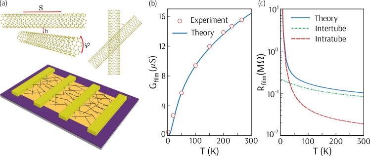
Here we study macroscopic assemblies of carbon nanotubes (CNTs), which provide an ideal model system in which to address the above issues and questions. Since their discovery in the early 1990s,Iijima (1991); Iijima and Ichihashi (1993); Bethune et al. (1993) extensive studies have revealed and established the truly unique electronic and optical properties of these one-dimensional nano-objects, particularly on individual nanotube levels. Depending on the precise atomic arrangements of -bonded carbon atoms in the honeycomb lattice, specified by a pair of integers called chirality indices, (,), both metallic and semiconducting species of CNTs exist; details of the band structure, most importantly the band gap, are determined by (,).Dresselhaus et al. (2001); Avouris et al. (2007, 2008); Nanot et al. (2013); Weisman and Kono (2019) Intertube electronic transport has also been studied theoreticallyNakanishi and Ando (2001); Buldum and Lu (2001); Maarouf and Mele (2011) and experimentally.(Fuhrer et al., 2000a, b) Based on the momentum-matching conditions on the initial and final states of electrons in a transfer between two individual CNTs with a crossing angle (see Figure 1a), the existence of special values of , where the intertube conductance becomes maximum and minimum has been identified Nakanishi and Ando (2001); Buldum and Lu (2001); Maarouf and Mele (2011). We show that after structural relaxation in a CNT- crossing geometry, the overall junction conductance increases by an order of magnitude with a quantitatively similar crossing angle dependence. Moreover, following Reference 19 for twisted bilayer phonon-assisted junction conductance, we demonstrate here that the intertube phonon-assisted junction conductance at room temperature is comparable to the pure electronic conductance. At some crossing angles, phonon-assisted junction conductance exceeds its electronic counterpart by an order of magnitude. These two effects – geometry relaxation and the additional phonon-assisted mechanism – enable us to achieve better quantitative agreement with prior experimentsFuhrer et al. (2000a) as well as the data reported here.
In our previous work,(Gao et al., 2021) we investigated the temperature dependence of conductivity in a set of macroscopic single-chirality CNT films with well-defined (,). Distinctly (,)-dependent and strongly temperature-dependent conductivity was observed, and the overall behaviors were explained through the Mott variable range hopping (VRH) model in a wide temperature range. However, one of the samples – an armchair (6,6) CNT film – exhibited clear deviation from the VRH behavior, especially at elevated temperatures, indicating that a different transport mechanism was at work. Through detailed quantitative analysis of the temperature-dependent conductivity, we found that the localization length was longer in (6,6) CNT film than in the other chirality samples such that intertube transport, as opposed to intratube transport, dominated in the (6,6) film at high temperatures. Here, through modeling and calculations of both electronic and phonon-assisted junction conductances, we unambiguously identify phonon-assisted conduction as the dominant mechanism for the observed high-temperature transport behaviour. The clear manifestation of this coherent dynamic process makes a single-chirality armchair CNT film a unique macroscopic object in which to study quantum transport processes at room temperature.
The device we used in this study was based on a thin film of randomly oriented, chirality-enriched (6,6) CNTs. The device had four electrodes, and the channel between the two inner electrodes, shown in the bottom panel of Figure 1a, had a length (), width (), and thickness () of 8 m, 5 m, and 12 nm, respectively. Further experimental details are fully described in Reference 20. The experimentally measured film conductance, , which is equal to the film conductivity times , is plotted against temperature in Figure 1b, showing that monotonically but sublinearly increases with temperature as the temperature is raised from 4.2 K to 300 K.
To understand the observed temperature dependence of the film conductance, we consider a series resistance model of the CNT conductivity and junction resistance, which contribute to the overall resistance of the film asShim et al. (2015a):
| (1) |
where the first and second terms originate from the intratube conductivity and the intertube junction conductance , respectively. A geometrical prefactor, , is determined by the average number of junctions in the film, where is the CNT diameter, is the interlayer distance between CNTs, and is the average length of CNTs. If we assume that the average crossing angle in a randomly oriented CNT film is , should be , according to our geometry, while the best fit to the data was obtained for , as shown in Figure 1b.
A temperature-dependent film conductance can arise from various sources. Our previous study on single-chirality CNT filmsGao et al. (2021) has shown that VRH is the dominant mechanism at low temperatures. Therefore, we model by the 1D Mott VRH model(Gao et al., 2021), i.e., . In Figure 1b, the theory curve according to Equation (1) includes the electronic and phonon-assistant contributions to the intertube (junction) conductance (discussed below) as well as the intratube conductivity. Since the sample is randomly oriented and the junction conductance depends on the angle (see Figure 1a), we averaged the intertube junction conductance over between and . The relative contributions of the intratube and intertube resistances are shown in Figure 1c. At temperatures below 50 K, the intratube resistance dominates, whereas, at temperatures above 50 K, the intertube junction resistance gives a dominant contribution to the film resistance.
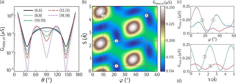
Below we discuss calculations of the intertube junction conductance. In the case of an ideally transparent contact, the maximum intertube conductance equals S. However, an experimentally measured conductanceFuhrer et al. (2000a) is substantially smaller; therefore, we use perturbation theory (see Methods) to calculate the intertube junction conductance as a sum of two parallel channels: electronic conductance due to the overlap of orbitals on neighboring tubes described by the tight-binding model and phonon-assistant conductance (see Methods). Since the distance between -orbitals in neighboring CNTs determines the hopping overlap, intertube junction conductance varies with the CNT structure registry. Atomic positions in an unrelaxed structure depend on the crossing angle (), rotation angle (), and sliding shift () between adjacent CNTs; see Figure 1a. In Figure 2a we show for an unrelaxed structure versus crossing angle in different armchair CNTs, including (6,6) CNTs; can vary by more than two orders of magnitude as changes. Figures 2b–2d show that varies with and by about 30% in (6,6) CNTs. Figure 2b is a surface map of versus and with , while Figures 2c and 2d are detailed and dependences of , corresponding to the labeled solid lines () in Figure 2b. The variation of with and are periodic with periods of and 2.46 Å, respectively, and hence, in Figure 2a was obtained as an average over and .
The large-diameter limit of can be understood by considering the junction conductance between twisted graphene bilayers,Maarouf and Mele (2011) where the momentum conservation law of electrons in two Brillouin zones twisted with respect to each other by angle governs the tunneling probability. However, in smaller-diameter CNTs, finite curvature plays an important role such that the finite contact area between the CNTs breaks the translation symmetry and helps relax the momentum conservation requirement. As a result, the conductance variations with angles diminish in magnitude, and a local minimum at vanishes in small-diameter armchair CNTs, as shown in Figure 2a.
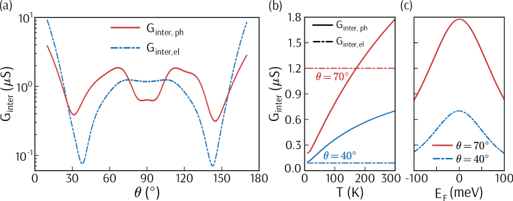
To better simulate the experimental situation, we relaxed the atomic positions at the junction using an atomistic valence force modelPerebeinos and Tersoff (2009) for the internal distortions in each CNT and the Lennard-Jones potential for atoms on adjacent CNTs. We set the van der Waals adhesion energy to meV per atomZacharia et al. (2004) and the interlayer graphene bilayer spacing to Å. The of the relaxed structure is increased by an order of magnitude compared to the unrelaxed case; this arises from the fact that more atoms on neighboring CNTs get closer due to CNT bending in the contact area. Figure 3a depicts the and of the relaxed structure versus , showing that overall they are comparable in magnitude at room temperature. The dependence of is weaker than that of because phonons help relax the momentum conservation law. Note also that the and dependences of the conductance do not enter into consideration for the relaxed structure.
The temperature dependence of phonon-assisted conductance is nearly linear in Figure 3b, reflecting the fact that low energy phonons are responsible for the phonon-assisted conductance, while the electronic intertube conductance is independent of temperature. The crossover temperature at which the two contributions become equal depends on the crossing angle. At angles near , the phonon-assisted contribution dominates the intertube conductance for almost all temperatures, whereas at the electronic contribution is larger even at room temperature, as shown in Figures 3a and b.
Finally, Figure 3c show the calculated Fermi energy dependence of . A small variation of the with the Fermi energy in Figure 3c reflects the fact that electron-phonon matrix elements have a weak momentum dependence and densities of electronic states are constant. In the case of electronic intertube conductance, we find that is almost independent of the Fermi energy (not shown).
In summary, we demonstrated that the temperature dependence of CNT film conductivity depend both on intratube and intertube (or junction) electronic transport. The dominant conduction mechanism depends on the film preparation conditions and the electronic structure of the CNTs.Gao et al. (2021) In this study, we showed that in films with a long localization length, such as a chirality-enriched (6,6) CNT film, the temperature dependence of the junction conductance can give rise to the observed overall temperature dependence of the CNT film conductance over a wide temperature range. We evaluated the temperature-independent electronic junction conductance and the temperature-dependent phonon-assisted junction conductance using microscopic theory, as shown in Figure 3. Our numerical results show that both contributions are important at room temperature, and depending on the crossing angle, the phonon-assisted junction conductance can be significantly larger than the electronic intertube conductance. After averaging over the CNT crossing angle, our model accurately reproduces the experimental data over a wide temperature range with a single parameter fit known from the film device dimensions. We found that structural relaxation increases the electronic conductance by an order of magnitude, making calculated results more consistent with prior experimental results of junction conductance at low temperatures.Fuhrer et al. (2000a) While the overall qualitative agreement between our model and the measured film conductance is evident, the nearly perfect quantitative agreement is likely accidental because of the oversimplified model used to estimate the numerical value of the parameter in Equation (1). At the same time, we underestimate by a factor of three the intertube conductance measured on individual CNTs,Fuhrer et al. (2000a) which could be due to a lack of angle control in the experiment. However, there can be a more fundamental reason for the observed discrepancy: the role of short-range defects in CNTs on the electronic and phonon-assistant intertube junction conductance, which should be a subject of further theoretical and experimental studies. Our work on chirality-enriched films provides guidelines for reinterpretation and analysis of other CNT network film resistances with the interplay of CNTs intratube transport and intertube junction transport.
I Methods
Conductance of 2D film:
As the thickness of the film is much smaller than the averaged length of SWCNT (), the film can be considered to be a 2D film. Then, the number of junctions for each percolation path can be estimated by assuming a saw-type 1D chain of length made of CNT rodes with crossing angle of . The number of parallel percolation paths over width can be estimated as and the number of 2D layers of CNT monolayers in a film of thickness can be estimated as . If each junction contributes a conductance of , then the total conductance due to the junctions in the film should be:
| (2) |
If we consider the conductance contribution from the nanotubes themselves (i.e., the intratube conductance), we can estimate it as follows:
| (3) |
where is the average distance that electron travels in the random film to reach from one electrode to the other and is the intratube conductivity. The net resistance of the 2D film can be estimated as:Shim et al. (2015a)
| (4) | |||||
which leads to an estimate of the value in Eq. (1). Note that the value in this simple model does not depend on the CNT volume density as opposed to more sophisticated models Komori and Makishima (1977); Shim et al. (2015b); Tripathy et al. (2020). In our model, CNT volume density is given by consistent with an estimate in Ref. Gao et al. (2021).
Electronic Intertube Junction Conductance:
The electronic conductance can be evaluated by Datta (2005)
| (5) |
where the spin degeneracy is included. Here, is the 2D electron wave vector in 2D Brillouin zone corresponding to periodically repeated supercell containing a single junction. labels the band index, , , , and are the elementary electronic charge, the reduced Plank constant, the applied voltage bias between layers, and the Fermi-Dirac distribution function, respectively. The intertube coupling is given by
| (6) |
where is the tunneling matrix element for carrier scattering from state to state on different CNTs. is the carrier energy, calculated by the tight-binding method with the first nearest-neighbor hoping eV. is the electron intertube interaction Hamiltonian due to the hopping between atoms on different CNTs. The hopping parameter is defined as (Perebeinos et al., 2012)
| (7) |
where Å is the equilibrium interlayer distance, is the distance between atoms and , Å, Å, , and eV. is the projection of onto the layers’ bisector, and its absolute value is given by
| (8) |
is the angle between and , , where is determined by (Perebeinos and Tersoff, 2009)
| (9) |
where , , and are the three nearest neighbors of . is perpendicular to the surface of the CNT, and its direction points toward the outside of CNT, and is perpendicular to .
Phonon-Assisted Intertube Junction Conductance:
The phonon-assisted conductance is computed by (Perebeinos et al., 2012)
| (10) |
Here, is given by
| (11) | ||||
where is the Bose-Einstein function, is the electron-phonon matrix element, and is the phonon frequency with wave vector and branch number . To obtain the phonon frequency, the structure is relaxed using the BFGS algorithm of the quasi-Newton method.Avriel (2003) The electron-phonon Hamiltonian are extracted by expanding Equation (7) in atomic displacements corresponding to the phonon normal modes.
Acknowledgements.
We gratefully acknowledge funding from the Vice President for Research and Economic Development (VPRED), SUNY Research Seed Grant Program, and computational facilities at the Center for Computational Research at the University at Buffalo (http://hdl.handle.net/10477/79221). A.M. and J.K. acknowledge support by the Basic Energy Science (BES) program of the U.S. Department of Energy through Grant No. DE-FG02-06ER46308 (for preparation of carbon nanotube films) and the Robert A. Welch Foundation through Grant No. C-1509 (for structural and electrical characterization measurements).References
- Jariwala et al. (2013) D. Jariwala, V. K. Sangwan, L. J. Lauhon, T. J. Marks, and M. C. Hersam, Chem. Soc. Rev. 42, 2824 (2013).
- Okimoto et al. (2010) H. Okimoto, T. Takenobu, K. Yanagi, Y. Miyata, H. Shimotani, H. Kataura, and Y. Iwasa, Advanced Materials 22, 3981 (2010).
- Rao et al. (2018) R. Rao, C. L. Pint, A. E. Islam, R. S. Weatherup, S. Hofmann, E. R. Meshot, F. Wu, C. Zhou, N. Dee, P. B. Amama, J. Carpena-Nuñez, W. Shi, D. L. Plata, E. S. Penev, B. I. Yakobson, P. B. Balbuena, C. Bichara, D. N. Futaba, S. Noda, H. Shin, K. S. Kim, B. Simard, F. Mirri, M. Pasquali, F. Fornasiero, E. I. Kauppinen, M. Arnold, B. A. Cola, P. Nikolaev, S. Arepalli, H.-M. Cheng, D. N. Zakharov, E. A. Stach, J. Zhang, F. Wei, M. Terrones, D. B. Geohegan, B. Maruyama, S. Maruyama, Y. Li, W. W. Adams, and A. J. Hart, ACS Nano 12, 11756 (2018).
- Gao et al. (2020) W. Gao, N. Komatsu, L. W. Taylor, G. V. Naik, K. Yanagi, M. Pasquali, and J. Kono, J. Phys. D 53, 063001 (2020).
- Zorn and Zaumseil (2021) N. F. Zorn and J. Zaumseil, Applied Physics Reviews 8, 041318 (2021).
- Iijima (1991) S. Iijima, Nature 354, 56 (1991).
- Iijima and Ichihashi (1993) S. Iijima and T. Ichihashi, Nature 363, 603 (1993).
- Bethune et al. (1993) D. S. Bethune, C. H. Kiang, M. S. de Vries, G. Gorman, R. Savoy, J. Vazquez, and R. Beyers, Nature 363, 605 (1993).
- Dresselhaus et al. (2001) M. S. Dresselhaus, G. Dresselhaus, and P. Avouris, eds., Carbon Nanotubes: Synthesis, Structure, Properties, and Applications, Topics in Applied Physics No. 18 (Springer, Berlin, 2001).
- Avouris et al. (2007) P. Avouris, Z. Chen, and V. Perebeinos, Nat. Nanotechnol. 2, 605 (2007).
- Avouris et al. (2008) P. Avouris, M. Freitag, and V. Perebeinos, Nat. Photon. 2, 341 (2008).
- Nanot et al. (2013) S. Nanot, N. A. Thompson, J.-H. Kim, X. Wang, W. D. Rice, E. H. Hároz, Y. Ganesan, C. L. Pint, and J. Kono, in Handbook of Nanomaterials, edited by R. Vajtai (Springer, Berlin, 2013) pp. 105–146.
- Weisman and Kono (2019) R. B. Weisman and J. Kono, eds., Optical Properties of Carbon Nanotubes: A Volume Dedicated to the Memory of Professor Mildred Dresselhaus (World Scientific, Singapore, 2019).
- Nakanishi and Ando (2001) T. Nakanishi and T. Ando, J. Phys. Soc. Jpn. 70, 1647 (2001).
- Buldum and Lu (2001) A. Buldum and J. P. Lu, Phys. Rev. B 63, 161403 (2001).
- Maarouf and Mele (2011) A. A. Maarouf and E. J. Mele, Phys. Rev. B 83, 045402 (2011).
- Fuhrer et al. (2000a) M. S. Fuhrer, J. Nygård, L. Shih, M. Forero, Y.-G. Yoon, H. J. Choi, J. Ihm, S. G. Louie, A. Zettl, and P. L. McEuen, Science 288, 494 (2000a).
- Fuhrer et al. (2000b) M. Fuhrer, A. K. Lim, L. Shih, U. Varadarajan, A. Zettl, and P. L. McEuen, Physica E: Low-dimensional Systems and Nanostructures 6, 868 (2000b).
- Perebeinos et al. (2012) V. Perebeinos, J. Tersoff, and P. Avouris, Phys. Rev. Lett. 109, 236604 (2012).
- Gao et al. (2021) W. Gao, D. Adinehloo, X. Li, A. Mojibpour, Y. Yomogida, A. Hirano, T. Tanaka, H. Kataura, M. Zheng, V. Perebeinos, and J. Kono, Carbon 183, 774 (2021).
- Shim et al. (2015a) W. Shim, Y. Kwon, S.-Y. Jeon, and W.-R. Yu, Sci. Rep. 5, 1 (2015a).
- Perebeinos and Tersoff (2009) V. Perebeinos and J. Tersoff, Phys. Rev. B 79, 241409 (2009).
- Zacharia et al. (2004) R. Zacharia, H. Ulbricht, and T. Hertel, Phys. Rev. B 69, 155406 (2004).
- Komori and Makishima (1977) T. Komori and K. Makishima, Textile Research Journal 47, 13 (1977).
- Shim et al. (2015b) W. Shim, Y. Kwon, S.-Y. Jeon, and W.-R. Yu, Scientific Reports 5, 16568 (2015b).
- Tripathy et al. (2020) S. Tripathy, B. Bose, P. P. Chakrabarti, and T. K. Bhattacharyya, IEEE Transactions on Electron Devices 67, 5676 (2020).
- Datta (2005) S. Datta, Quantum Transport: Atom to Transistor (Cambridge University Press, 2005).
- Avriel (2003) M. Avriel, Nonlinear Programming: Analysis and Methods (Courier Corporation, 2003).