N2, NO and O2 molecules in LiGaO2 in both Ga and Li sites and their relation to the vacancies.
Abstract
Doping of the ultrawide band gap semicodnctor LiGaO2 ( eV) with N2, NO and O2 molecules placed in either Ga or Li-vacancies is studied using first-principles calculations. These molecular dopants are considered as potential acceptors for -type doping. Their optimal placement and orientation relative to the lattice is studied as well as their transition levels and energy of formation. Unfortunately, they are found to have deep acceptor level transition states. We discuss the relation of the transition levels to the one-electron levels, their spin state and defect wave functions. They are found to be closely related to those of the corresponding vacancies.
I Introduction
LiGaO2 was recently proposed to be a promising ultrawide band gap semiconductor. Its band gap is 5.6 eV as verified by optical absorption measurements [1, 2, 3] and QS (quasiparticle self-consistent ) calculatons.[4, 5] Similar to -Ga2O3 density functional theory (DFT) calculations calculations using a hybrid functional HSE06 predict that this material could be -type doped by Si or Ge, which form shallow donors.[6, 7] On the other hand, comparing to -Ga2O3, it has a larger gap, somewhat lower valence band masses and a simpler wurtzite related crystal structure, the structure,[8] in which all atoms are tetraehedrally coordinated. It can be grown in bulk form.[9]
In the only study thus far of the doping opportunities,[7] -type doping was still found to be problematic, as is also the case for its parent compound ZnO and for many other oxides, including -Ga2O3. Standard candidate acceptor dopants like NO were found to give too deep levels in the gap and in fact in this case amphoteric character. Zn in LiGaO2 on the other hand suffers from site competition between the acceptor ZnGa and donor ZnLi. Thus, more involved schemes need to be pursued for establishing -type doping. Here we take some inspiration from previous work in ZnO. [10] In ZnO, it is known that a shallow acceptor exists[11] that is related to N but is not the simple substitutional defect. Several candidates have been suggested. Lautenschlaeger [12] proposed that H is involved in a complex. Bang et al. [13] proposed doping with NH3 and a NH3 on the Zn-site. Boonchun and Lambrecht proposed a N2 molecule on a Zn-site,[10]. Another model is a N complex.[14]
The latter was shown to be possible to incorporate making use of the surface chemistry of adsorption of N on a ZnO O-terminated Zn-polar surface. In that case, N incorporates preferentially on the Zn sites but then leads to a O-vacancy in the next layer. After this N complex is burried inside the sample, the N can easily overcome a barrier and interchange places and hop into the adjacent thereby creating the desired complex, which was found to be shallow. This scheme was made to work in practice by a careful sequence of growth and annealing treatments by Reynolds et al.[15, 16] and is perhaps one of the most promising routes to -type doping in ZnO.
The alternative proposed scheme with N2 has not yet been pursued experimentally. It is based on the idea of aligning the molecular levels of N2 with those in ZnO. A N2 molecule has 10 valence electrons (22) in its neutral charge state and is extremely stable because all the and bonding states are filled. When placed in a Zn site, it needs to act as a ion and thus compared with Zn including the filled -band which lies at about the same energy as the deeper N2 molecule -bonds, it lacks 2 electrons compared to Zn2+. This implies it is a double acceptor. In the single negative charge state of the defect, (N2) state it would correspond to a N molecule. This state with an unpaired spin has been observed clearly in Electron Paramagnetic Resonance (EPR) [17] although these authors assumed it was located on a O-site. However, Boonchun and Lambrecht[10] showed that on the O-site it would behave as a donor and demonstrated that the Zn-site has qualitatively the correct -tensor and hyperfine splitting. While they proposed it is a shallow acceptor and thus suitable for -type doping, that depends somewhat on the choice of functional and later calculations by Petretto and Bruneval[18] found a somewhat different location of the N2 molecule more strongly bonded to the surrounding O of the which behaved as a deep acceptor. An experimental study of the recharging behavior of the N2 in ZnO also proposed that it is a deep center.[19] Nonetheless, the verdict on the shallow or deep nature of this defect center is still out and there are alternative explanations for the observed behavior. For example, there might be both a deep and a shallow configuration of the defect depending on how strongly the N2 bonds to the O surrounding it. Rotational entropy might favor the less strongly bound form at higher temperatures and the charging/recharging behavior of the defect taking into account the higher charge states of the defect has not yet been studied in detail by computational means.
Here we extend the idea of N2 incorporation on a cation site to LiGaO2. There are some differences with the corresponding system in ZnO. In LiGaO2, the N2 on a Ga site would be a triple acceptor instead of a double acceptor. The Ga- level lies much deeper than the Zn- so the alignment with the N2 molecular levels might be different. The is a defect of high energy of formation, so it might be less easy to obtain N2 in this site, but the has low energy of formation. The alignment of the molecular levels with the host levels is not a-priori clear and is investigated here. Here we study N2, NO and O2 as molecular doping species on both cation vacancy sites and evaluate their formation energy, structural optimization for different orientations of the molecule and their transition levels.
II Computational Methods
Our study is based on density functional calculations (DFT) using the Heyd-Scuseria-Ernzerhof (HSE) hybrid functional[20, 21] with the standard fraction of exact screened Hartree-Fock type exchange = 0.25 and range parameter of = 10 Å, giving a gap of = 5.1 eV slightly smaller than the experimental value.[22, 23, 24, 25] Since this work extends our previous published results, we keep the computational approach used here the same as in [6] and [7]. The calculations are performed within the Vienna Ab-Initio Simulation Package (VASP).[26, 27] The electron ion interactions are described by means of the Projector Augmented Wave (PAW) method.[28, 29] We use a well-converged energy cutoff of 500 eV for the projector augmented plane waves. The dopants are modeled in a 128-atom supercell, for which a shifted single k-point Brillouin zone sampling was found to be sufficiently converged.
The analysis of the defect levels follows the standard defect approach as outlined in e.g. Freysoldt et al. [30] The energy of formation of the defect in charge state is given by
| (1) |
where is the total energy of the supercell containing the defect and is the total energy of the perfect crystal supercell. The energy for adding or removing atoms from the crystal to a reservoir in the process of producing the defect is represented by the chemical potentials . The chemical potentials of the host elements that we chose are presented in our previous paper.[6] The value represents the change in the number of atoms in the species . For the impurities, the chemical potential of N is calculated from the total energy per atom of an isolated N2 molecule, where the chemical potential of O is fixed which respect to the extreme condition as reported in the previous study.[6] The alignment and image charge corrections are calculated using the Freysoldt approach.[31] These energies of formation are used to study the transition levels between different charge states, each with fully relaxed structures but kept at the same volume.
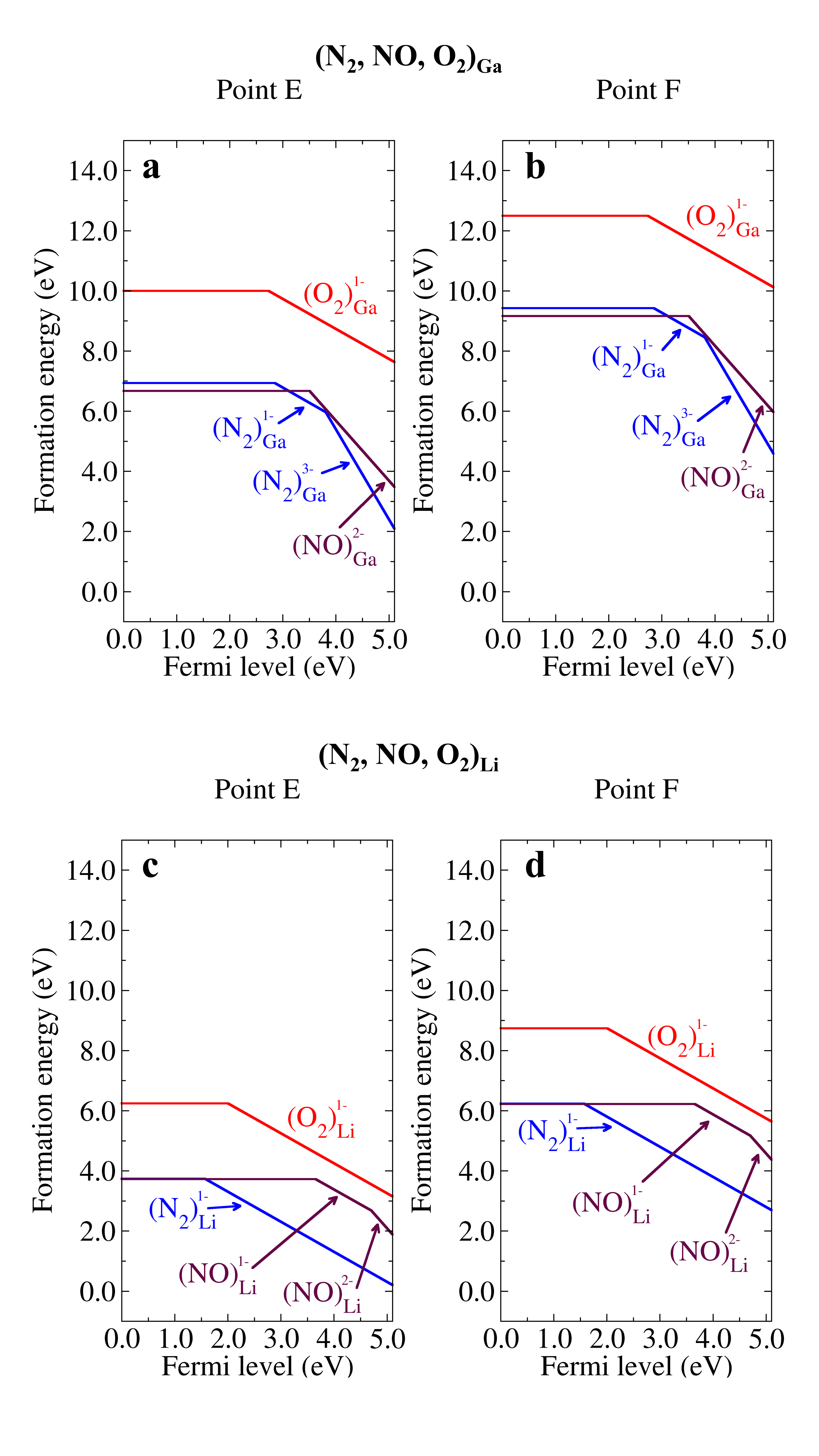
The formation energies of , and are plotted as function of Fermi level in Fig.2 for chemical potential conditions E and F. Note that chemical potential conditions E and F (see figure 2 in Ref. 6) correspond respectively to more Li-rich and more Ga-rich conditions but restricted by the formation of competing binary compounds. Realistic conditions on the O chemical potential corresponding to the typical growth temperature are used in both cases. The absolute chemical potentials at point E are eV, eV and eV, while the absolute chemical potentials at point F are eV, eV and eV.
The absolute chemical potentials used for the dopants are eV. However, the formation energies of all three impurities are high with this choice of chemical potentials E and F, implying low solubility in LiGaO2.
III Results
III.1 Structural models and relaxation.
For each molecule we study various configurations of the relative orientation of the molecule relative to the crystal and fully relax them. For the N2 and O2 cases, we have first positioned N2 and O2 along the original bond of Ga and O. Both of and , they can be categorized into planar configurations (P1, P2 and P3) and vertical configuration (V1) as shown in Fig.S1 in supplementary information (SI). Similarly to the NO case, the initial position of NO was set along the original Ga-O bond. In this case, we have 6 initial planar structures (planar (P1-a, P1-b, P2-a, P2-b, P3-a, and P3-b) and 2 vertical structures (V1-a and V1-b) as shown in Fig.S2 in SI. The reason why there are more structural models is that for the case, we need to distinguish how the dipole of the the NO molecule is directed.
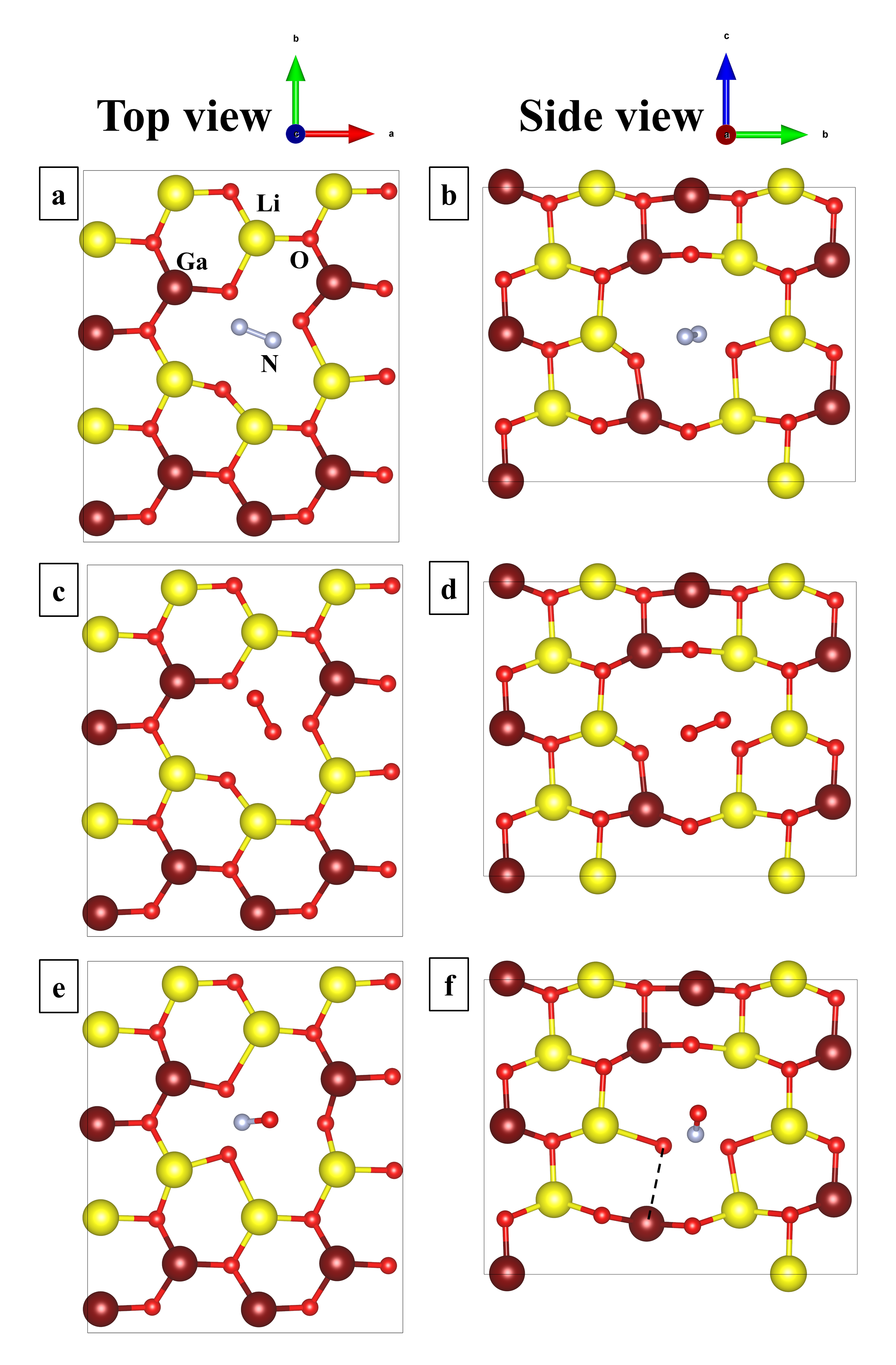
Next, we found that the most energetically favourable is the P3 arrangement in the case of N2 and O2. The optimized structure of and are presented in Fig.1(a)-(d). In the top view, we can see only a slight shift of the positions, but in the side view we may notice a larger shift of the N2 or O2 molecule from their initial positions. For the NO-case, the most energetically favorable is the P2-a arrangement. The optimized structure is presented in Fig.1(e)-(f). Compared to the N2 and O2 cases, we here see a larger distortion of the O atoms surrounding the vacancy both in the top and side views. One of the O below has significantly moved closer to the N atom of the NO to the expense of weakening its bond with the next nearest neighbor Ga.
III.2 Energies of formation and transition levels
The energies of formation for different charge states, choosing the configuration with lowest structural energy are given in Fig. 2 for two cases of chemical potentials, more Li-rich (E) and more Ga-rich (F) cases. Both points are chosen to pick a realistic O chemical potential corresponding to the growth conditions as explained in Ref. 6.
They show first that the energies of formation on the Ga site (Fig.2(a)-(b)) are relatively high. The reason for this is simply that the Ga vacancy itself is a high-energy of formation defect as reported in our previous study.[6] One could in principle still realize these defect cases by first creating vacancies using for example high-energy irradiation and subsequently introduce the dopants by reactions from the surface inwards, by exposure to N2, NO or O2 gas.
Second, they show that N2 occurs in three charge states depending on the position of the Fermi level, neutral, and . This indicates a negative behavior between and charge states. Interestingly, in the corresponding Ga-vacancy, the charge state also has already a narrow energy range of stability. Likewise, NO occurs in neutral and charge states only. However, O2 occurs only in neutral and charge states and exhibits no negative- behavior.
Third, the transition levels all are quite deep with the lowest transition level occurring at about 2.85 eV above the valence band maximum (VBM) for the N2 case.
The energy of formation results for the various molecules on the Li site are given in Fig.2(c)-(d). These have slightly lower energies of formation consistent with the lower energy of formation of the as reported in our previous study.[6] Structurally, there is ample room for these molecules in both types of vacancy sites. The transition levels are slightly shallower for the Li site occupation. For example, the transition level for (N2)Li is 1.57 eV instead of (N2)Ga where it is 2.85 eV. The (N2)Li exists only in 0 and states and the same holds for the O2 case, while the NO molecule exists in three charge states, 0, , .
III.3 One-electron levels and defect wave functions.
In this section, we examine the one-electron levels, their defect wave functions, and partial densities of states (PDOS) to clarify the spin states of the defects and their relation to the transition levels.
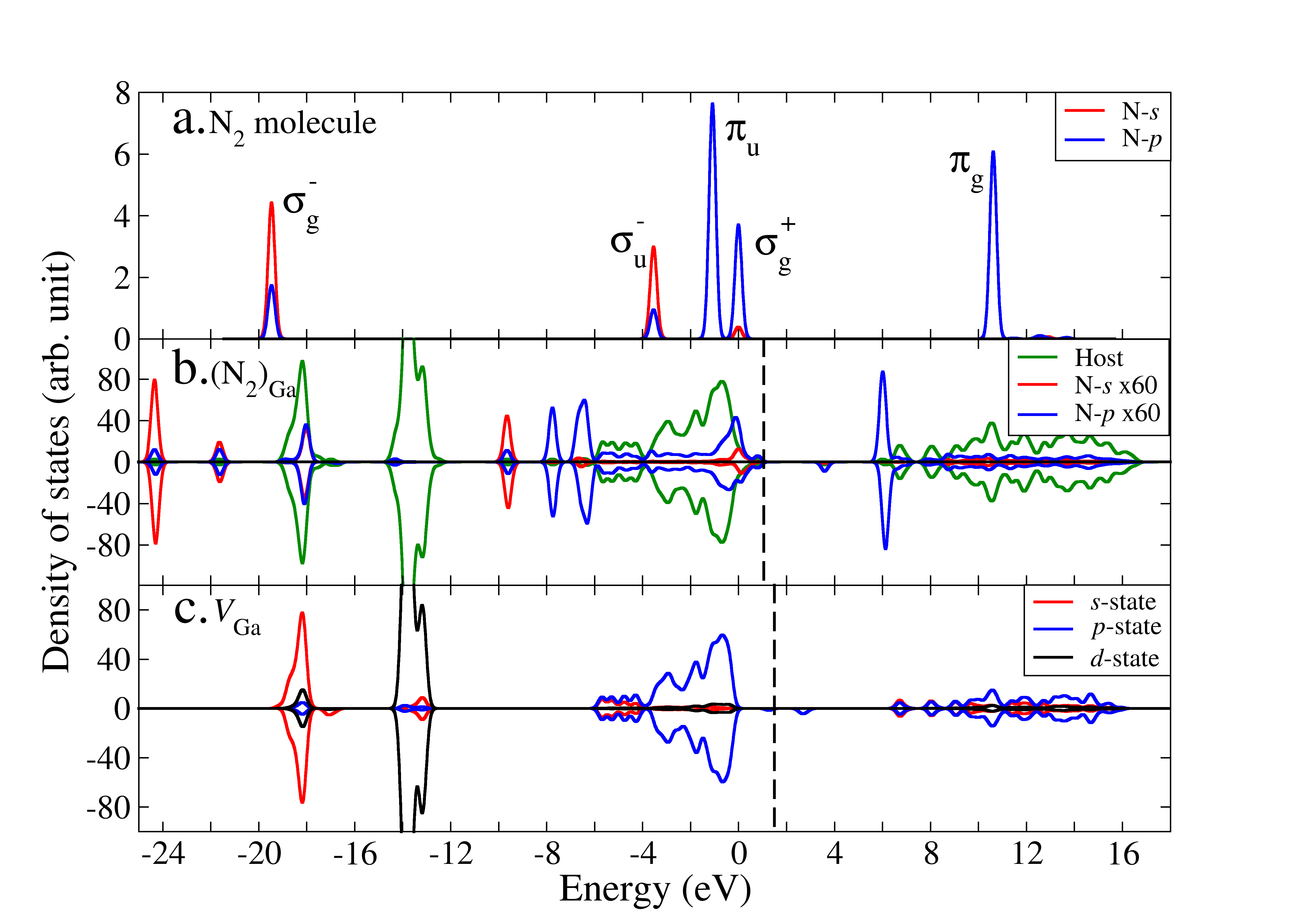
In Fig. 3 we show the PDOS of N2 placed in the Ga-vacancy in panel (b), while panels (a) and (c) show the isolated molecule and the Ga-vacancy PDOS respectively. In panel (a), we have labeled the peaks according to the standared nomenclature for molecular eigenstates. First, we recognize the lowest empty molecular orbital (LUMO) antibonding state lying above 10 eV. Next, the state forms the highest occupied molecular orbital (HOMO). We see that it consists mostly of N- orbitals with a small N- contribution. The HOMO-1 level is the bonding state, which has pure character and is doubly degenerate and thus has twice the peak height of the HOMO. The next level is the state which is a bonding state between N- and N-. Its antibonding counter part lies at higher energy above the CBM and is not shown. The state at eV is the bonding counterpart to the state and has mostly N- character with a little bit of N-. Here, the labels refer to even or odd with respect to inversion and refers to (anti)bonding character. We need this extra label only for states because there is more than one and . From panel (b) we can see that there is a net spin-polarization in the neutral charge state, which is related to its odd number of electrons. We can still clearly recognize the antibonding state of the N2 molecule, lying at the conduction band minimum (CBM). A minority spin state is seen at mid gap and states of both majority and minority spin character occur just above the VBM. We here aligned the deep O- states with those of the host system containing the Ga-vacancy shown in panel (c) and indicate the Fermi level at zero temperature (highest occupied state) by the dashed line. We can see several defect levels of minority spin also in panel (c) for the neutral Ga-vacancy with only the lowest one of these occupied. These levels look dangling bond like (see Fig.S6 in SI) but are spread over several neighboring O sites.
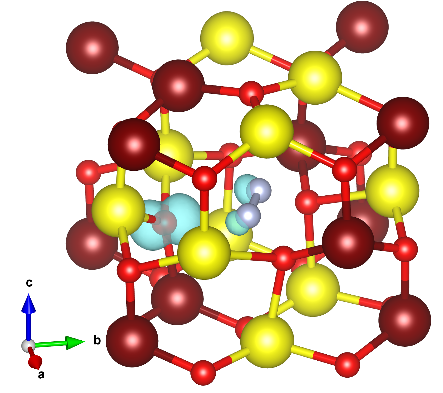
The N- projected PDOS of the N2 molecule inside the Ga-vacancy shows a peak about 1 eV below the VBM with a net difference between spin-up and spin down, indicating that part of the spin density must be localized on the molecule. However, the bonding state of the molecule are more perturbed by the interaction with the host. It appears that this state forms both bonding and antibonding states with the O- valence states with the bonding states lying just below the O- bands and the antibonding ones slightly below the VBM. In fact, we find three peaks localized on the molecule lying just below the O- valence band, two with predominantly N- character and one with predominantly N- character. The state in the molecule has pure character but when placed in the Ga-vacancy it acquires a small amount of character and the peak height is now the same as for the state because its weight is also partially found in the states just below the VBM and distributed to some extent throughout the valence band. The states near eV are seen to be the Ga- states and some hybridization between the deep lying states with the O- band can also be seen. All of this indicates a significant interaction between the molecular states and the vacancy states. The net spin density in the neutral charge state of (N2)Ga is shown in Fig. 4 and confirms this picture.
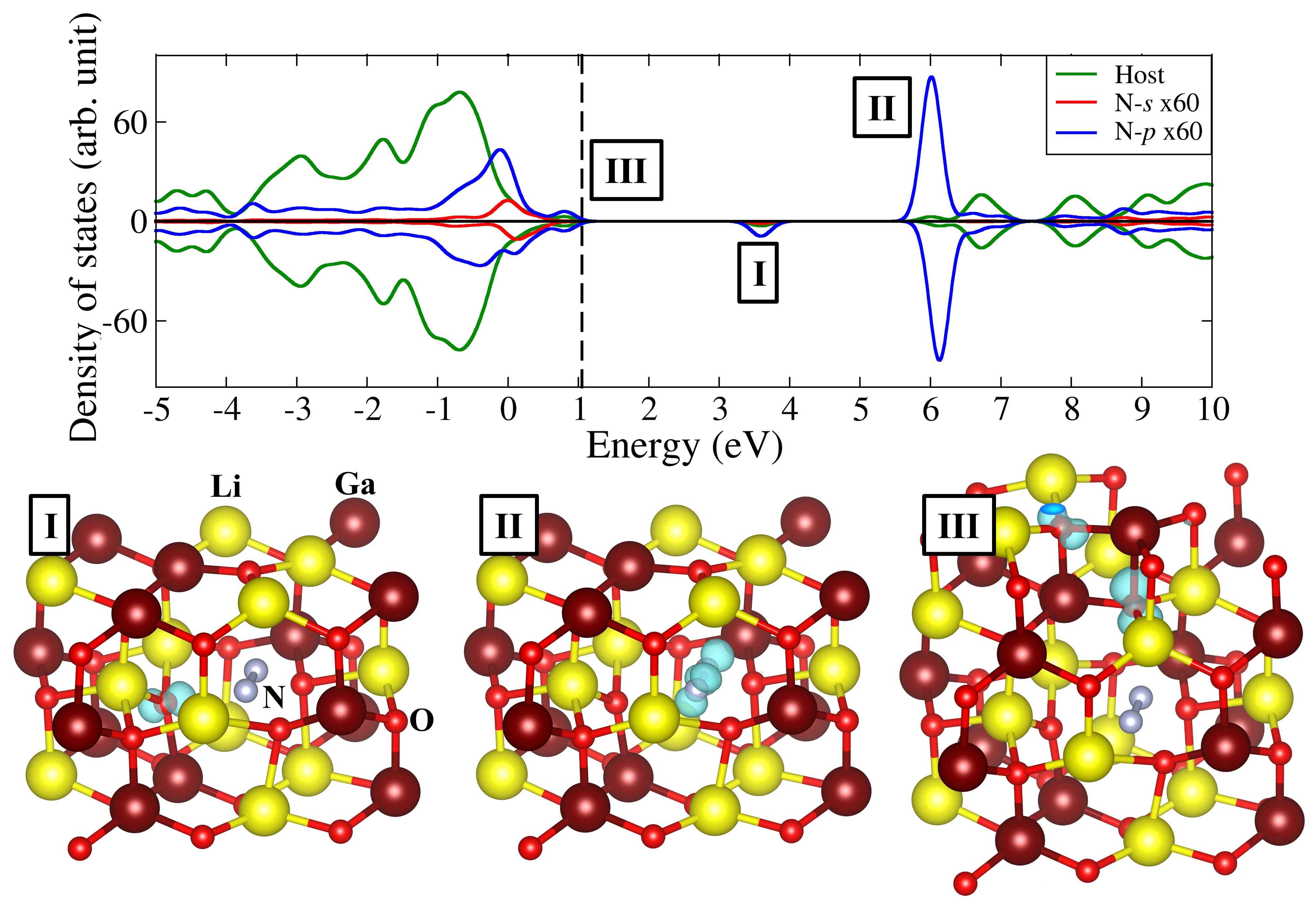
In Fig.5, we show the partial densities of states (PDOS) and defect wavefunctions modulo squared for several energy ranges corresponding to defect levels for the N2 on Ga site. We note several defect levels or resonances in the bands introduced by the molecule insertion into the vacancy. First, the state (labeled II) corresponds clearly to the molecular antibonding state and lies just below the CBM of the host crystal. A resonance also occurs just below the VBM and corresponds to the highest occupied molecular orbital (HOMO) of the N2 molecule and has -bonding character. In addition to these molecular levels, we recognize a defect level (labeled I) which is localized on one of the O surrounding the defects. It is accompanied by a polaronic distortion localizing the wave function on only one of the O nearest neighbors of the Ga vacancy in which the N2 is inserted. A defect level closer to the VBM, (labeled III) still shows also localization on one of the nearest neighbor oxygens but spreads somewhat further to further neighbor O. All of these were obtained for the neutral defect.
For the N2 on the Ga site, which has 3 holes in the defect or molecule levels compared to the perfect crystal since it can exist also in -1, -2 and -3 charge states by successively adding electrons, we have also examined the possibility of a higher spin state with three parallel spins. This configuration, however, was found to have 1.53 eV higher energy and can thus safely be excluded from further consideration. We find from the corresponding PDOS that the N- related states occur deeper below the VBM, as shown in Fig.S6 in SI.
For N2 placed on the Li-site we similarly show the comparison between the N2 PDOS in the isolated molecule and in the Li site and with the Li-vacancy case, again, all for the neutral charge state. The state is again most readily identified as lying near the CBM at about 6 eV. Defect states related to the Li-vacancy are also found in the gap. However, in this case the N2 HOMO state is located near the bottom of the O- states and much less interaction is observed than for the Ga-vacancy. This indicates a different electrostatic potential in which the N2 molecule finds itself. In fact, it is a less repulsive potential because removing a Li+ is less repulsive than removing a Ga3+, thereby placing these states deeper relative to the O- bands. The molecular states are thus differently aligned with respect to the LiGaO2 host bands when the N2 is located in the Ga than in the Li vacancy. A weaker interaction is also observed for the deep state with the O- band. There is is still a net spin-density as shown in Fig. 7.
Until now we have focused on the neutral charge state and on the N2 molecule related states and their interaction with their surroundings. However, it is also clear that several states exist in the gap and inspection of their wave functions shows that these states are primarily localized on a single oxygen and are closely related to the corresponding vacancy states. Adding an electron in the negative charge states makes the system non-spin polarized as there is now an even number of electrons. We checked that the high-spin configuration for the charge state has higher energy by 1.05 eV. Again, we find that the occupied one-electron states of the N2 molecule occur farther below the VBM. We can study the addition of an electron in two steps, first keeping the structure frozen in that of the neutral charge state and subsequently relaxing the atomic positions. We find that the levels in the gap are spread deeper into the conduction band in the frozen geometry of the neutral state and move closer to the VBM upon relaxation. This is shown in Fig.S8 in the SI. Likewise in the charge state, we have again a net spin polarization and so on. After filling the empty states of the molecule, the next electrons essentially are located in the vacancy related dangling bond states and correspond closely to the corresponding vacancy case. However for the we find several states with localization on more than one O-neighbor to the vacancy.
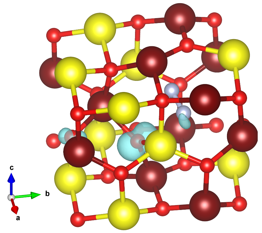
The one-electron energy levels lying inside the band gap are shown in Fig.8 as function of charge state. They are shown for both spin states. One can see that in the neutral charge state only one defect level (No. 415 ) close to the VBM (levels 414 for and spin) is occupied while three remain empty. In the charge state, the lower one of these, which is the minority spin level 415, is lowered significantly while it becomes occupied. Likewise, in the and charge states, additional levels come down in energy as they become occupied. This reflects the fact that in hybrid functional, due to the partial inclusion of exact exchange, the potential is orbital-dependent and occupied levels shift down relative to empty levels.
We should here caution the reader that these one-electron levels, also seen as peaks in the PDOS, reflect the band positions in the 128 cell model, which is not truly reflective of the dilute limit. An electrostatic correction applies to the single particle levels for charged defect states due to their interaction with the image charges and the neutralizing background, similar to the well-known corrections to the energies of formation. These corrections allow one to extrapolate to the dilute limit and would shift the one-electron levels of the isolated defect deeper into the gap with a shift proportional to their charge and inversely proportional the size of the supercell . Here is a Madelung constant and is the dielectric constant of the host. Because these defect one-electron levels are pushed deeper in the gap than indicated by the PDOS, filling them only occurs when the Fermi level is also rather deep in the gap and this essentially explains the deep nature of the transition levels even though rather shallow states are seen in the PDOS figures or for the occupied one-electron levels.
We can further examine the PDOS of these different charge states and the associated wave functions. These details are given in Fig.S9 in the SI for charge states -1,-2, -3. The main conclusion is that the peaks in the PDOS can be associated with the levels given in Fig. 8 and their associated states show mostly vacancy type localized states with in some cases a partial contribution on the molecule and for states closer to the VBM a wider spread farther away from the defect site. We thus find that the states in the gap are closely related to those of the corresponding vacancy and have generally the character of dangling bond states on the surrounding oxygen atoms. The relaxation tends to localize them on a single oxygen rather than being distributed over several oxygens. This indicates the polaronic nature of these defect states.
Moving on to the NO and O2 as inserted molecules, the changes can basically be understood in terms of the added valence electron in each step. The PDOS of the NO and O2 on the Ga and Li site in the neutral charge state are shown in SI. They indicate that the NO molecule in the neutral charge state is similar to the N2 in the state and the O2 molecule in the neutral state is similar to the N2 in the state. The defect levels in the gap in all these cases are mostly localized on a single oxygen neighbor of the vacancy in which the molecule is placed.
IV Discussion
In the present calculations, we find deep levels and polaronic acceptor behavior for each of these molecules when inserted in either a Li or Ga vacancy. This is manifested in the localization of the defect wave functions each time on a single O. In part, this behavior is emphasized by the hybrid functional choice. All of these results were obtained with the standard HSE setting of 25 % exact exchange. As a final check on our results, we therefore investigated the satisfaction of the generalized Koopmans theorem (gKT) by calculating the non-Koopman’s energy[32],
| (2) |
where is a localized state’s Kohn-Sham quasiparticle energy in an N electron system, is the system’s ionization energy, which is equivalent to the difference between the total energies and of the N and N-1 electron systems with defect, respectively. In the Table 1, we calculated the non-Koopman’s energy () for 20%, 25% and 30% HF mixing parameters from our previous SnGa calculation.[7] In the case of the gKT, should equal be zero. As a result, we found that for 30% HF mixing parameter is almost zero (-0.012 eV), indicating that gKT is fulfilled. Moreover, the energy gap from this calculation is very close to the experiment value as presented in Table 1. Although this indicates that a 30 % HF would have been preferable, we have kept the 25 % results to be consistent with our previous papers. Even for the 25% HF mixing parameter, is already relatively small (-0.121 eV), thus the self-interaction error may be considered small in all the present calculations.
| HF mixing parameter | ||||
|---|---|---|---|---|
| 20% | 25% | 30% | Exp. value | |
| (eV) | 4.70 | 5.10 | 5.50 | 5.3-5.6[22, 23, 24, 25] |
| (eV) | 3.818 | 4.010 | 4.070 | |
| (eV) | 4.057 | 4.132 | 4.082 | |
| (eV) | -0.240 | -0.121 | -0.012 | |
V Conclusions
In this paper we have examined the behavior of inserted diatomic molecules N2, NO and O2 in both the Li and Ga site. We found that these systems have high energy of formation, especially for the Ga site, which is related to the corresponding vacancy formation energy. Even though these systems all behave as acceptor systems, we found deep transition levels in the gap, which are not compatible with -type doping. Analysis of the PDOS and one-electron levels shows that as successive levels become occupied in the negative charge states, they move closer to the VBM. This is a direct result of the hybrid functional used which lowers occupied vs. empty levels. While the occupied ones appear much shallower than the transition levels, this is an artifact of the supercell size. Corrections for the one-electron levels in charged systems will tend to move these levels deeper in the gap proportional to their charge state, so that the transition levels and one-electron levels become consistent with each other in labeling these systems as deep acceptors. The behavior of NO and O2 in charge state correspond to the corresponding , states of N2. We find a stronger interaction of the N2 molecular states with the O-states of the host for the Ga than for the Li position in terms of the occupied states of the molecule. The defect levels in the gap are closely related to the corresponding vacancy levels and are dangling bond like and characterized by polaronic distortions localizing the defect wave functions on a single O neighbor to the vacancy. We find that the Koopmans theorem is already fairly well satisfied by the 25 % exact exchange hybrid functional used here and in our previous work on native defects, although in future work a 30 % model would both improve the band gap and the satisfaction of Koopmans theorem.
Acknowledgements.
The work at CWRU was supported by the U.S. National Science Foundation under grant No. 1755479. K.D. was supported by the National Research Council of Thailand (NRCT), No. NRCT5-RGJ63002-028. A.B. has been funded by the Office of National Higher Education Science Research and Innovation Policy Council (NXPO), Thailand, through Program Management Unit for Competitiveness (PMU C), Contract Number C10F630073. Calculations were in part performed at the Ohio Supercomputer Center.References
- Wolan and Hoflund [1998a] J. T. Wolan and G. B. Hoflund, “Chemical alteration of the native oxide layer on LiGaO2(001) by exposure to hyperthermal atomic hydrogen,” J. Vac. Sci. Tech. A 16, 3414–3419 (1998a).
- Johnson, McLeod, and Moewes [2011a] N. W. Johnson, J. A. McLeod, and A. Moewes, “The electronic structure of lithium metagallate,” Journal of Physics: Condensed Matter 23, 445501 (2011a).
- Chen et al. [2014a] C. Chen, C.-A. Li, S.-H. Yu, and M. M. Chou, “Growth and characterization of -LiGaO2 single crystal,” Journal of Crystal Growth 402, 325 – 329 (2014a).
- Radha, Ratnaparkhe, and Lambrecht [2021] S. K. Radha, A. Ratnaparkhe, and W. R. L. Lambrecht, “Quasiparticle self-consistent band structures and high-pressure phase transitions of and ,” Phys. Rev. B 103, 045201 (2021).
- Boonchun and Lambrecht [2011] A. Boonchun and W. R. L. Lambrecht, “Electronic structure, doping, and lattice dynamics of LiGaO2,” in Oxide-based Materials and Devices II, Proceedings of SPIE, Vol. 7940, edited by F. H. Terani, D. C. Look, and D. J. Rogers, International Society for Optics and Photonics (SPIE, 2011) pp. 129–134.
- Boonchun, Dabsamut, and Lambrecht [2019] A. Boonchun, K. Dabsamut, and W. R. L. Lambrecht, “First-principles study of point defects in LiGaO2,” Journal of Applied Physics 126, 155703 (2019).
- Dabsamut, Boonchun, and Lambrecht [2020] K. Dabsamut, A. Boonchun, and W. R. L. Lambrecht, “First-principles study of n- and p-type doping opportunities in LiGaO2,” Journal of Physics D: Applied Physics (2020).
- Marezio [1965] M. Marezio, “The crystal structure of LiGaO2,” Acta Crystallographica 18, 481–484 (1965).
- Ishii, Tazoh, and Miyazawa [1998] T. Ishii, Y. Tazoh, and S. Miyazawa, “Single-crystal growth of LiGaO2 for a substrate of GaN thin films,” J. Crystal Growth 186, 409 – 419 (1998).
- Lambrecht and Boonchun [2013] W. R. L. Lambrecht and A. Boonchun, “Identification of a N-related shallow acceptor and electron paramagnetic resonance center in ZnO: N on the Zn site,” Phys. Rev. B 87, 195207 (2013).
- Zeuner et al. [2002] A. Zeuner, H. Alves, D. Hofmann, B. Meyer, A. Hoffmann, U. Haboeck, M. Strassburg, and M. Dworzak, “Optical Properties of the Nitrogen Acceptor in Epitaxial ZnO,” physica status solidi (b) 234, R7–R9 (2002).
- Lautenschlaeger et al. [2011] S. Lautenschlaeger, M. Hofmann, S. Eisermann, G. Haas, M. Pinnisch, A. Laufer, and B. K. Meyer, “A model for acceptor doping in ZnO based on nitrogen pair formation,” physica status solidi (b) 248, 1217–1221 (2011).
- Bang et al. [2015] J. Bang, Y.-Y. Sun, D. West, B. K. Meyer, and S. Zhang, “Molecular doping of ZnO by ammonia: a possible shallow acceptor,” J. Mater. Chem. C 3, 339–344 (2015).
- Liu et al. [2012] L. Liu, J. Xu, D. Wang, M. Jiang, S. Wang, B. Li, Z. Zhang, D. Zhao, C.-X. Shan, B. Yao, and D. Z. Shen, “-Type Conductivity in N-Doped ZnO: The Role of the Complex,” Phys. Rev. Lett. 108, 215501 (2012).
- Reynolds et al. [2013] J. G. Reynolds, C. L. Reynolds, A. Mohanta, J. F. Muth, J. E. Rowe, H. O. Everitt, and D. E. Aspnes, “Shallow acceptor complexes in p-type ZnO,” Applied Physics Letters 102, 152114 (2013).
- Reynolds and Reynolds [2014] J. G. Reynolds and C. L. Reynolds, “Progress in ZnO Acceptor Doping: What Is the Best Strategy?” Advances in Condensed Matter Physics 2014, 457058 (2014).
- Garces et al. [2003] N. Y. Garces, L. Wang, N. C. Giles, L. E. Halliburton, G. Cantwell, and D. B. Eason, “Molecular nitrogen (N2-) acceptors and isolated nitrogen (N-) acceptors in ZnO crystals,” Journal of Applied Physics 94, 519–524 (2003).
- Petretto and Bruneval [2014] G. Petretto and F. Bruneval, “Comprehensive Ab Initio Study of Doping in Bulk ZnO with Group-V Elements,” Phys. Rev. Applied 1, 024005 (2014).
- Philipps et al. [2014] J. M. Philipps, J. E. Stehr, I. Buyanova, M. C. Tarun, M. D. McCluskey, B. K. Meyer, and D. M. Hofmann, “Recharging behavior of nitrogen-centers in ZnO,” Journal of Applied Physics 116, 063701 (2014).
- Heyd, Scuseria, and Ernzerhof [2003] J. Heyd, G. E. Scuseria, and M. Ernzerhof, “Hybrid functionals based on a screened Coulomb potential,” J. Chem. Phys. 118, 8207–8215 (2003).
- Heyd, Scuseria, and Ernzerhof [2006] J. Heyd, G. E. Scuseria, and M. Ernzerhof, “Erratum: “Hybrid functionals based on a screened Coulomb potential” [J. Chem. Phys. 118, 8207 (2003)],” J. Chem. Phys. 124, 219906 (2006).
- Wolan and Hoflund [1998b] J. T. Wolan and G. B. Hoflund, “Chemical alteration of the native oxide layer on ligao 2 (001) by exposure to hyperthermal atomic hydrogen,” Journal of Vacuum Science & Technology A: Vacuum, Surfaces, and Films 16, 3414–3419 (1998b).
- Johnson, McLeod, and Moewes [2011b] N. Johnson, J. McLeod, and A. Moewes, “The electronic structure of lithium metagallate,” Journal of Physics: Condensed Matter 23, 445501 (2011b).
- Ohkubo et al. [2002] I. Ohkubo, C. Hirose, K. Tamura, J. Nishii, H. Saito, H. Koinuma, P. Ahemt, T. Chikyow, T. Ishii, S. Miyazawa, et al., “Heteroepitaxial growth of -ligao 2 thin films on zno,” Journal of applied physics 92, 5587–5589 (2002).
- Chen et al. [2014b] C. Chen, C.-A. Li, S.-H. Yu, and M. M. Chou, “Growth and characterization of -ligao2 single crystal,” Journal of crystal growth 402, 325–329 (2014b).
- [26] https://www.vasp.at/.
- Kresse and Furthmiiller [1996] G. Kresse and J. Furthmiiller, “Efficiency of ab-initio total energy calculations for metals and semiconductors using a plane-wave basis set,” Computational Materials Science 6, 15–50 (1996).
- Blöchl [1994] P. E. Blöchl, “Projector augmented-wave method,” Phys. Rev. B 50, 17953–17979 (1994).
- Kresse and Joubert [1999] G. Kresse and D. Joubert, “From ultrasoft pseudopotentials to the projector augmented-wave method,” Phys. Rev. B 59, 1758–1775 (1999).
- Freysoldt et al. [2014] C. Freysoldt, B. Grabowski, T. Hickel, J. Neugebauer, G. Kresse, A. Janotti, and C. G. Van de Walle, “First-principles calculations for point defects in solids,” Rev. Mod. Phys. 86, 253–305 (2014).
- Freysoldt, Neugebauer, and Van de Walle [2009] C. Freysoldt, J. Neugebauer, and C. G. Van de Walle, “Fully Ab Initio finite-size corrections for charged-defect supercell calculations,” Phys. Rev. Lett. 102, 016402 (2009).
- Ivády et al. [2013] V. Ivády, I. Abrikosov, E. Janzén, and A. Gali, “Role of screening in the density functional applied to transition-metal defects in semiconductors,” Physical Review B 87, 205201 (2013).