Also at ]Physics Department, Florida Sate University
Resistively loaded coplanar waveguide for microwave measurements of induced carriers
Abstract
We describe the use of a coplanar waveguide whose slots are filled with resistive film, a resistively loaded coplanar waveguide (RLCPW), to measure two dimensional electron systems (2DES). The RLCPW applied to the sample hosting the 2DES provides a uniform metallic surface serving as a gate, to control the areal charge density of the 2DES. As a demonstration of this technique we present measurements on a Si MOSFET, and a model that successfully converts microwave transmission coefficients into conductivity of a nearby 2DES capacitively coupled to the RLCPW. We also describe the process of fabricating the highly resistive metal film required for fabrication of the RLCPW.
I Introduction
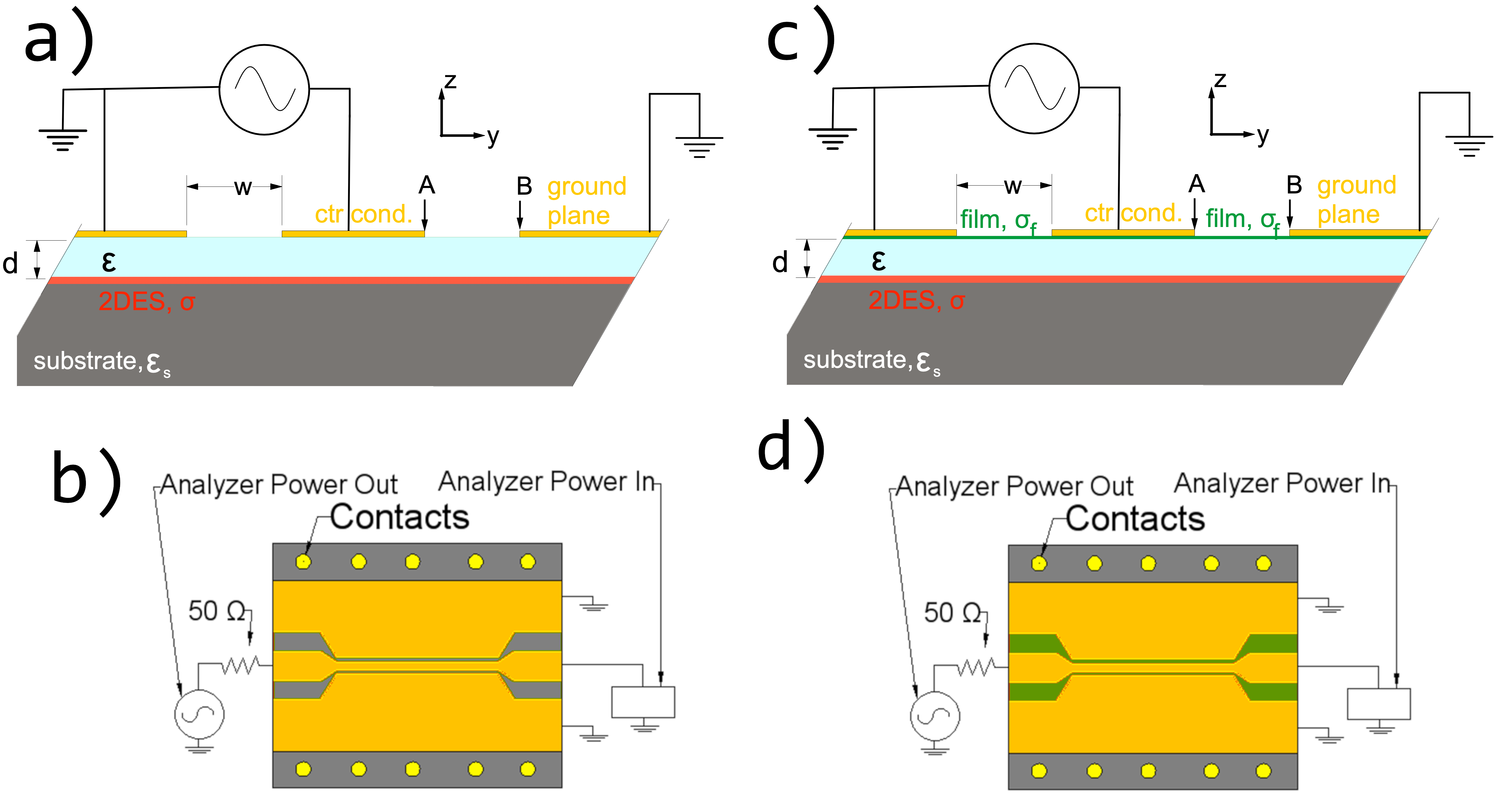
Coplanar waveguide (CPW) is a standard and well-characterized type of microwave transmission line, which has the advantage of being constructed on a single plane. A CPW, as shown in Fig. 1a and b, is constructed of metal film forming a driven center conductor and broad ground planes, separated by slots. Placing a CPW in capacitive or direct contact with a two-dimensional electron system (2DES) allows broadband measurements of absorption and phase shift due to the 2DES. CPW-based microwave spectroscopy of this sort has been performed on 2DES hosted in semiconductors [1, 2, 3, 4, 5] and on large-area graphene [6, 7, 8]. In these measurements the transmission through the CPW is particularly sensitive to the conductivity of the 2DES under the slot regions of the CPW.
In studying 2DES it is often necessary to vary the density of the system by means of biasing a metallic gate. Some semiconductor-hosted 2DES, as well as high quality graphene and transition metal dichalcogenides are not charged by deliberately placed dopants, but rely on charge induced by a gate. Such gates, if in close proximity to the 2DES, create complications for CPW based microwave measurements, because a highly conducting gate screens the microwave electric field, reducing the sensitivity to changes in the conductivity of the 2DES. One approach to this problem has been to fabricate gates spaced away from the CPW and the 2DES, and biasing these gates with high voltage. This method [3] was performed with a front gate, spaced by a vacuum (or air) gap and a thin glass plate above the CPW in Fig. 1a, and also with gates on the back side of a semiconductor wafer (far below the CPW in the figure). When the spaced front gate is used, the density in the slots and under the CPW metal is mismatched unless the 2DES is biased precisely relative to the CPW to match the the density in the slots; such matching is difficult in practice. Both the back and spaced front gates have limited range of density tunability, require high bias voltage, and do not work in some samples. Another approach, which uses a highly conductive gate combined with a sensitive density modulation technique to detect cyclotron resonance, is described by ref. 4.
In this paper we demonstrate microwave measurements using a resistively loaded CPW (RLCPW), as shown in Fig. 1c and d, in which a resistive film gate is placed under the highly conductive CPW conductors, and only partly screens the microwave field. This is analogous to the use of semitransparent gates in optical experiments. Our motivation for this is experimentation in heterojunction insulated gate field effect transistors (HIGFETS)[9, 10, 11, 12, 13] which are semiconductor devices known to give particularly low disorder and wide density tunability. However, for the proof-of-concept demonstration in this paper we present data on a Si metal-oxide-semiconductor field-effect transistor (MOSFET), a well-understood device whose large disorder is expected to render its conductivity nearly independent of frequency in our measuring range.
The RLCPW retains the advantages of wide bandwidth and coplanar (single-surface) construction, but presents a uniform surface to the sample. In semiconductors this removes density gradiant due to Schottky potentials, and reduces strain due to differential contraction relative to a conventional CPW. Microwave measurements can couple capacitively to samples, so in that case are essentially contactless, though a single contact to a sample (possibly only at elevated temperature) is required to induce the carriers. The contact, which can be challenging in undoped devices, can be highly resistive, with a leak of or more sufficient to populate most samples. A limitation of the RLCPW measurement is that it becomes insensitive if the 2DES conductivity is much less than that of the resistive film, so fabricating a high resistivity film in the RLCPW is an important aspect of the design. In the following we describe fabrication and measurement of an RLCPW with high resistivity metal film on the Si MOSFET. In addition we present an analytical model for conversion of microwave transmission measurement to a 2DES conductivity for the capacitively coupled case, and compare its results to the measurements.
II Experiment set-up and MOSFET device
Figure 1d shows a schematic of the experiment with a top view of the RLCPW, which we fabricated as a gate on a MOSFET with oxide thickness of 35 nm. The edges of the RLCPW are tapered to facilitate a low-reflectance connection to microstrip lines on kapton film, which are in turn connected to coaxial cables. The length of the RLCPW between the tapers is 2.5 mm, the center conductor width is 45 m, and the slot width () is 30 m. The sample is located in a 0.3 K cryostat, and is connected to a room-temperature network analyzer, which serves as transmitter and receiver. Ohmic contacts on the device enable dc measurements of the MOSFET, and allow the 2D channel to be populated by the gate.
For the purpose of charging the channel, the RLCPW can be regarded as a uniform gate. (The microwave voltage applied between the RLCPW center line and its ground planes is much smaller than the dc bias voltages.) For convenience of the microwave connections, the RLCPW is grounded to the cryostat, and we apply negative bias () to the contacts of the MOSFET relative to that ground to populate the channel. The device substrate is lightly p-type doped with a room temperature resistivity of 1-10 . This lightly doped substrate freezes out at low temperatures and minimizes microwave absorption at our measuring temperature of 0.3 K. The properties of the oxide layer of the MOSFET are important for the model calculation of conductivity from microwave absorption: the MOSFET had oxide thickness of 35 nm and we took the oxide dielectric constant to be 3.7.
Resistive film
A key component of the RLCPW is the resistive film. Here we used a recently developed thin film composed of evaporated Ge, Ni, and Pt layers[14]. The thicknesses of the Ge, Ni, and Pt layers were 20, 0.5, and 1 nm, respectively. After deposition, the film was annealed in a forming gas environment at 525 C for 10 sec. This thermal treatment created a resistive film with a resistivity on the order of 1-10 k/square [14]. In this work, we obtained the 2D resistivity of the film, square, from the dc resistance between the center conductor and the ground planes, making use of the much higher conductivity of the side planes and center conductor.
III Experimental Results
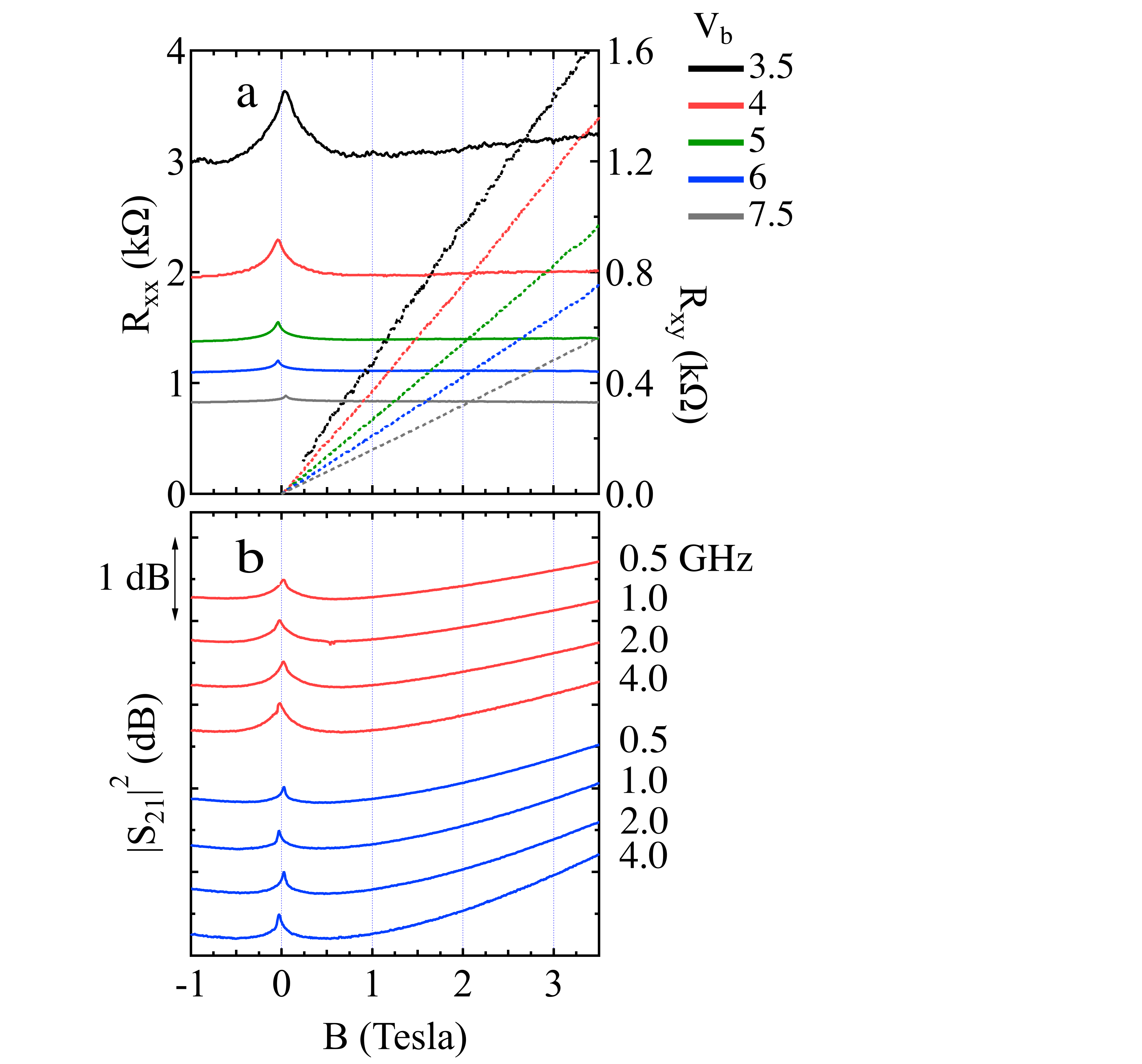
Using the ohmic contacts, we characterize the MOSFET by standard techniques of dc transport, for different as magnetic field () is varied. Figure 2a shows the diagonal and Hall resistances, and vs , for several bias voltages. As is increased, decreases and the slope of the Hall resistance decreases due to increasing 2D density, (shown below in Fig. 4a). The Hall resistance follows the classical formula . Prominent in these and subsequent traces vs magnetic field is a peak at due to weak localization; the apparent slight displacement of this peak from in some traces is an artifact of remanent field in the superconducting magnet.
Figure 2b shows the microwave transmission at various frequencies (), for and V. Unlike the dc curves of panel a, the curves exhibit an upward curvature which arises because the transmission is sensitive to rather than . The traces are offset from each other for clarity, and their dependence changes little for the different frequencies. Measurements with long thin transmission lines are nearly insensitive to , as has been shown for measurements in the quantum Hall regime [1].
IV Analytical Model
The model presented here can be used to calculate complex transmission coefficient [15] from a 2DES conductivity, given the dimensions of the RLCPW, the film resistivity and the per unit area capacitance between the 2DES and the film. To convert measured to 2DES conductivity, the model must be inverted, which is conveniently done numerically. A more time-consuming alternative to the model is to use commercially available simulator software, such as Sonnet [16], which we used to check the analytical model.
Figure 1b shows a schematic cross section of the RLCPW system narrowly spaced above a 2DES. We model the system in the quasi-TEM approximation which is applicable to situations where the wavelength is much larger than the RLCPW slot width. Besides high frequency effects which become important when the wavelength approaches , the model neglects edge effects[17] and also the capacitance due to lines of force which terminate at both ends on the 2DES; both these effects are small for the RLCPW with achievable film resistivities. For , even with the smallest achievable film conductivity , these effects are not important. Quantum (density of states) capacitance[18] is neglected in this paper and is not important for the MOSFET device, but could be incorporated in the coupling capacitance when appropriate.
We consider a distributed circuit, composed of parallel plate transmission lines comprised of the 2DES and the metal above; this approach has been used elsewhere[19, 20]. In the present case the parallel plate lines are transverse ( direction in Fig. 1) to the RLCPW propagation direction ( in the figure, pointing toward the viewer of the figure) of the RLCPW. The parallel plate lines, whose top layer is the RLCPW and whose bottom layer is the 2DES have voltage and current related by
| (1) |
where primes indicate differentiation in . , pertain to the top layer RLCPW, and , to the 2DES. is the capacitance per unit area of the dielectric layer, given by , where is the dielectric thickness. is taken to be zero for the highly conductive center conductor and side planes, and for the region of the slots.
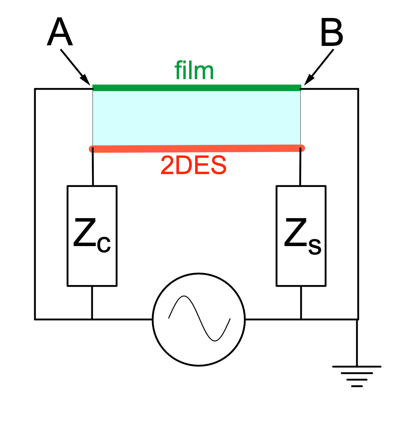
We calculate the complex transmission coefficient [15] using the circuit of Fig. 3 to obtain the load admittance per unit length in the propagation direction, presented to the RLCPW by the resistive film and by the capacitively coupled 2DES. In the figure, the impedances , , result from Eq. (1) applied to a side plane and the center conductor regions. The coupled resistive film and 2DES is between the points marked A and B in the figure. Here is taken for a wide side plane, assuming current vanishes within the ground plane as gets farther from the outer edge of the slot, and would need to be modified to include the outside boundary of the side plane in the case [19, 20] of low loss and large kinetic inductance.
| (2) |
With , , , and . Of the coefficients , obtained from solving this system, only is of interest, and gives the admittance due to the sample layer, per unit length in the propagation direction of the RLCPW, as .
We design the RLCPW in the quasi-TEM approximation such that if the sample layer and the resistive film were absent, the underlying CPW with characteristic impedance and phase velocity would result [21]. (Presently, this task can easily be performed for a substrate of known dielectric constant using online calculators [22].) The model for the RLCPW incorporates into the admittance per unit length in the propagation direction resulting in propagation constant and chararacteristic impedance . is normalized for a 50 measuring system, in which the complex transmission coefficient of the RLCPW is
| (3) |
V Microwave conductivity measurement with the RLCPW
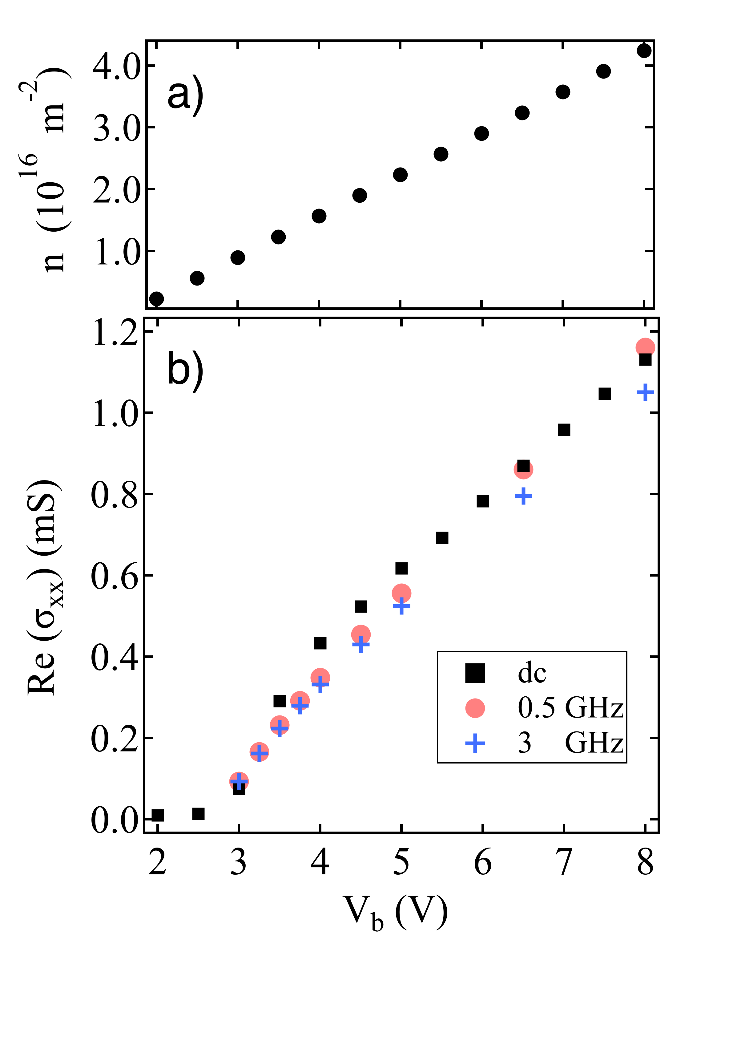
We demonstrate microwave conductivity measurement with the RLCPW by comparing microwave and dc conductivities, relying on the independence of the conductivity of the MOSFET on the frequency. The disorder in the MOSFET leads to a short carrier momentum relaxation time, . Frequency independence is expected when . Using , where is taken at zero frequency and field, and for Si the relevant effective mass free electron masses[23], we find seconds. Hence is satisfied for our measuring conditions ( GHz).
We use the dc data of Fig. 2a to test obtaining the 2DES conductivity from microwave measurements. The dc resistivity, is calculated by the van der Pauw method [24] from resistances obtained from different sets of ohmic contacts at the edges of the RLCPW. We find the dc from the tensor inversion, , where the part of that is antisymmetric about is .
Figure 4b shows real diagonal conductivities Re, vs , obtained from dc measurements through the contacts, and from measurements at frequencies of 0.5 and 3 GHz. To avoid the sharp weak localization feature in the conductivity, the data were taken with a 2 T magnetic field. To remove the frequency dependent effects of cables, the 0.5 and 3 GHz Re data shown were obtained with a simplified calibration procedure, assuming zero absorption from the 2DES at zero bias. We measured , and iteratively compared it to the results of the model of the previous section for varying , , taking the imaginary part of to be zero, as is appropriate for . The dc and microwave Re data are grouped together, demonstrating our main point that the RLCPW method can be used to obtain with appropriate modeling. There are several sources of discrepancies between the points of the three traces on the graph. First, dc resistivity measurements used to calculate Re probe different areas on the MOSFET than the RLCPW measurement, which reports conductivity as an average mainly from the areas under the RLCPW slots. The differences between the two microwave frequency data at larger Re may be due to the increase in reflection from the RLCPW which is not removed by the simple calibration procedure.
In summary, we have demonstrated that microwave-frequency measurements can be carried out with an RLCPW transmission line as a sample is gated with a resistive film to vary induced carrier density widely. We have shown that the conductivity of the gated 2DES can be obtained quantitatively from such measurements, by means of an analytic model into which the resistivity of the film loading the RLCPW is incorporated.
Acknowledgements.
The microwave measurements and sample design at NHMFL were supported by Department of Energy (Grant No. DE- FG02-05-ER46212). The National High Magnetic Field Laboratory is supported by the National Science Foundation Cooperative Agreement No. DMR-1644779 and the State of Florida. This work was partly funded by the U.S. Department of Energy (DOE) Office of Basic Energy Sciences (BESs). This work was performed, in part, at the Center for Integrated Nanotechnologies, a U.S. DOE, Office of BESs, user facility. Sandia National Laboratories is a multimission laboratory managed and operated by National Technology and Engineering Solutions of Sandia LLC, a wholly owned subsidiary of Honeywell International Inc. for the U.S. DOE’s National Nuclear Security Administration under contract DE-NA0003525. This paper describes objective technical results and analysis. Any subjective views or opinions that might be expressed in the paper do not necessarily represent the views of the U.S. DOE or the United States Government. The data that support the findings of this study are available from the corresponding authors upon reasonable request.References
- Engel et al. [1993] L. W. Engel, D. Shahar, Ç. Kurdak, and D. C. Tsui, “Microwave frequency dependence of integer quantum Hall effect: Evidence for finite-frequency scaling,” Phys. Rev. Lett. 71, 2638–2641 (1993).
- Sambandamurthy et al. [2006] G. Sambandamurthy, Z. Wang, R. M. Lewis, Y. P. Chen, L. W. Engel, D. C. Tsui, L. N. Pfeiffer, and K. W. West, “Pinning mode resonances of new phases of 2d electron systems in high magnetic fields,” Solid State Commun. 140, 100 – 106 (2006).
- Hatke et al. [2015] A. T. Hatke, Y. Liu, L. W. Engel, M. Shayegan, L. N. Pfeiffer, K. W. West, and K. W. Baldwin, “Microwave spectroscopic studies of the bilayer electron solid states at low Landau filling in a wide quantum well,” Nat. Commun. 6, 7071 (2015).
- Stone et al. [2012] K. Stone, R. R. Du, M. J. Manfra, L. N. Pfeiffer, and K. W. West, “Millimeter wave transmission spectroscopy of gated two-dimensional hole systems,” Applied Physics Letters 100, 192104 (2012).
- Drichko et al. [2014] I. L. Drichko, A. M. Diakonov, V. A. Malysh, I. Y. Smirnov, Y. M. Galperin, N. D. Ilyinskaya, A. A. Usikova, M. Kummer, and H. von Känel, “Contactless measurement of alternating current conductance in quantum hall structures,” Journal of Applied Physics 116, 154309 (2014).
- Dragoman et al. [2011] M. Dragoman, D. Neculoiu, A. Cismaru, A. A. Muller, G. Deligeorgis, G. Konstantinidis, D. Dragoman, and R. Plana, “Coplanar waveguide on graphene in the range 40 mhz–110 ghz,” Applied Physics Letters 99, 033112 (2011).
- Skulason et al. [2012] H. S. Skulason, H. V. Nguyen, A. Guermoune, M. Siaj, C. Caloz, and T. Szkopek, “Contactless impedance measurement of large-area high-quality graphene,” in 2012 IEEE/MTT-S International Microwave Symposium Digest (2012) pp. 1–3.
- Wu et al. [2016] Y. Wu, Y. Wu, K. Kang, Y. Chen, Y. Li, T. Chen, and Y. Xu, “Characterization of cvd graphene permittivity and conductivity in micro-/millimeter wave frequency range,” AIP Advances 6, 095014 (2016).
- Kane, Pfeiffer, and West [1995] B. E. Kane, L. N. Pfeiffer, and K. W. West, “High mobility GaAs heterostructure field effect transistor for nanofabrication in which dopant induced disorder is eliminated,” Applied Physics Letters 67, 1262–1264 (1995).
- Willett et al. [2007] R. L. Willett, M. J. Manfra, L. N. Pfeiffer, and K. W. West, “Mesoscopic structures and two-dimensional hole systems in fully field effect controlled heterostructures,” Applied Physics Letters 91, 033510 (2007).
- Sarkozy et al. [2009] S. Sarkozy, K. D. Gupta, C. Siegert, A. Ghosh, M. Pepper, I. Farrer, H. E. Beere, D. A. Ritchie, and G. A. C. Jones, “Low temperature transport in undoped mesoscopic structures,” Applied Physics Letters 94, 172105 (2009).
- Pan et al. [2016] W. Pan, K. W. Baldwin, K. W. West, L. N. Pfeiffer, and D. C. Tsui, “Antilevitation of landau levels in vanishing magnetic fields,” Phys. Rev. B 94, 161303 (2016).
- Pan et al. [2017] W. Pan, W. Kang, K. W. Baldwin, K. W. West, L. N. Pfeiffer, and D. C. Tsui, “Berry phase and anomalous transport of the composite fermions at the half-filled landau level,” Nature Physics 13, 1168–1172 (2017).
- Harris and Lu [2021] C. T. Harris and T.-M. Lu, “A PtNiGe resistance thermometer for cryogenic applications,” Review of Scientific Instruments 92, 054904 (2021).
- Adam [1969] S. F. Adam, “Microwave theory and applicaitons,” (Prentice-Hall, 1969).
- [16] From Sonnet Software, Syracuse, NY; www.sonnetsoftware.com.
- Fogler and Huse [2000] M. M. Fogler and D. A. Huse, “Dynamical response of a pinned two-dimensional wigner crystal,” Phys. Rev. B 62, 7553–7570 (2000).
- Eisenstein, Pfeiffer, and West [1994] J. P. Eisenstein, L. N. Pfeiffer, and K. W. West, “Compressibility of the two-dimensional electron gas: Measurements of the zero-field exchange energy and fractional quantum hall gap,” Phys. Rev. B 50, 1760–1778 (1994).
- Mehrotra and Dahm [1987] R. Mehrotra and A. J. Dahm, “Analysis of the sommer technique for measurement of the mobility for charges in two dimensions,” Journal of Low Temperature Physics 67, 115–121 (1987).
- Burke et al. [2000] P. J. Burke, I. B. Spielman, J. P. Eisenstein, L. N. Pfeiffer, and K. W. West, “High frequency conductivity of the high-mobility two-dimensional electron gas,” Applied Physics Letters 76, 745–747 (2000).
- Ghione and Naldi [1987] G. Ghione and C. Naldi, “Coplanar waveguides for mmic applications: Effect of upper shielding, conductor backing, finite-extent ground planes, and line-to-line coupling,” IEEE Transactions on Microwave Theory and Techniques 35, 260–267 (1987).
- [22] See, example, https://www.microwaves101.com/calculators/864-coplanar-waveguide-calculator.
- Sze [1981] S. M. Sze, “Physics of semiconductor devices,” (Wiley Interscience, 1981) p. 849, 2nd ed.
- Seeger [1988] K. Seeger, “Semiconductor physics: an introduction,” (Springer, 1988) p. 63, 4th ed.