Temperature Effect on Charge-state Transition Levels of Defects in Semiconductors
Abstract
Defects are crucial in determining the overall physical properties of semiconductors. Generally, the charge-state transition level α(q/q’), one of the key physical quantities that determines the dopability of defects in semiconductors, is temperature dependent. However, little is known about the temperature dependence of α(q/q’), and, as a result, almost all existing defect theories in semiconductors are built on a temperature-independent approximation. In this article, by deriving the basic formulas for temperature-dependent α(q/q’), we have established two fundamental rules for the temperature dependence of α(q/q’) in semiconductors. Based on these rules, surprisingly, it is found that the temperature dependences of α(q/q’) for different defects are rather diverse: it can become shallower, deeper, or stay unchanged. This defect-specific behavior is mainly determined by the synergistic or opposing effects between free energy corrections (determined by the local volume change around the defect during a charge-state transition) and band edge changes (which differ for different semiconductors). These basic formulas and rules, confirmed by a large number of state-of-the-art temperature-dependent defect calculations in GaN, may potentially be widely adopted as guidelines for understanding or optimizing doping behaviors in semiconductors at finite temperatures.
I. Introduction
Intrinsic defects and external impurities (generally denoted as defects hereafter) play a critical role in determining the physical properties of solids, e.g., from solar cells 1 ; 2 ; 3 to solid-state lighting 4 ; 5 to topological phase control 6 ; 7 ; 8 and to quantum computing 9 ; 10 ; 11 . The defect formation energies H(,q) for defect at charge state q, that determine the defect concentrations; and the charge-state transition levels α(q/q’), that correspond to the thermal ionization energies, are two of the most important physical quantities for all the defects in semiconductors 12 ; 13 ; 50 . Generally, both H(,q) and α(q/q’) are temperature dependent. Differing from the straightforward temperature dependence of H(,q) 12 ; 13 ; 14 ; 17 ; 18 , little is known about how temperature changes affect α(q/q’) in semiconductors, due to the lack of basic formulas and fundamental rules. As a result, almost all defect theories in semiconductors are built on static first-principles calculations excluding temperature effects 12 ; 13 ; 50 .
The challenge to unravel the temperature dependence of α(q/q’) in theory is two-fold. Fundamentally, the standard formulas for α(q/q’) calculations are incomplete and do not capture the α(q/q’) of defects under finite temperatures. Practically, the computations of temperature-induced vibrational properties of defects in semiconductors are extremely expensive. Because of its unparalleled complexity, the temperature dependence of α(q/q’) in semiconductors has remained unanswered for decades i.e., we do not have any rules to predict or understand the dopability of semiconductors at finite or changing temperatures.
Differing from narrow bandgap (NBG) semiconductors (e.g., Si and GaAs) that usually operate under ambient environments at room temperature, wide bandgap (WBG) semiconductors (e.g., GaN and SiC) can operate under harsh environments with high working temperatures 20 ; 21 ; 22 ; 23 ; 24 . Therefore, WBG semiconductors are an ideal platform for unique applications in aerospace, nuclear power and earth’s mantle investigation, that require changing operation temperatures from extremely-low to extremely-high (01000 K) 20 ; 21 ; 22 ; 23 ; 24 ; 25 ; 26 ; 27 ; 28 . This highlights the need to understand the evolution with temperature of defect properties in WBG semiconductors, especially of α(q/q’), which may be critical to improve the reliability of WBG semiconductor devices in various environments.
In this article, by deriving the basic formulas of temperature-dependent α(q/q’), we have established two fundamental rules for the temperature dependence of absolute and relative α(q/q’) in semiconductors, respectively. Based on these rules, it is found that regardless of the initial α(q/q’) levels at 0 K, surprisingly, the temperature-dependent behaviors of α(q/q’) for different defects in different types of semiconductors are rather diverse, i.e., it can become shallower, deeper, or even stay unchanged, mainly determined by the synergistic or opposing effects between free energy corrections and band edge changes. Importantly, we discover that the electronic and vibrational contributions to free energy corrections are both fundamentally determined by a key physical quantity V, the local volume change around the defect during the charge-state transition. Interestingly, the V values are mainly determined by the competing effect between the local electron occupation (LEO) changes and the strength of the local lattice relaxation (LLR) around the defects. Using the state-of-art first-principles-based temperature-dependent approaches with the capacity of both high accuracy and high efficiency 51 , these proposed basic formulas and fundamental rules have been thoroughly verified based on a large number of defect calculations in GaN.
II. Results and Discussion
A. Basic Formulas
Without the inclusion of temperature effects, the α(q/q’) of a defect between the charge-states q and q’ is given as
| ((1)) |
where E(,q) [E(,q’)] is the total energy of a supercell with defect in charge-state q [q’] and VBM(host) is the valence band maximum (VBM) of the host 12 ; 13 ; 50 . With the inclusion of temperature effects, E(,q) [E(,q’)] in Eq.(1) is replaced by the corresponding free energy F(,q) [F(,q’)]. After some manipulations [see Appendix A], it can be written as
| ((2)) |
On the right-hand side of Eq. (2), the second term represents the corrections from the free energy differences between the q and q’ configurations induced by the electronic (Fel) and vibrational (Fph) contributions, while the third term represents the correction on the VBM energy position driven by thermal expansion and electron-phonon coupling (VBM = thVBM+phVBM). In practice, the temperature dependence of α(q/q’) can be understood without and with the inclusion of VBM 45 , corresponding to the absolute and relative evolutions of α(q/q’), respectively. While the temperature dependence of the absolute α(q/q’) [aα(q/q’)] is solely determined by the free energy corrections, that of the relative α(q/q’) [rα(q/q’)] is determined by both the free energy corrections and the band edge changes. Although α(q/q’) is independent of the direction of charge-state transitions, to simplify our discussion, in the following we focus on the ionization process, i.e., |q’|>|q|. This assumption does not change the rules we developed.
Under the quasi-harmonic approximation (QHA), Fel can be written as Fel=Eth+Eel-TSel 13 ; 29 ; 30 , where the first, second, and third terms are the energy corrections induced by thermal expansion, electron-occupation change, and electronic entropy, respectively. Generally, the contributions from Eel and Sel to Fel are negligible under reasonable temperatures in semiconductors 12 ; 31 . Therefore, we focus on the Eth term in Fel. Without an external pressure, V=V T V0+V0, where V is the mean volumetric thermal expansion coefficient (usually, V>0) and V0 is the equilibrium volume at 0 K. Ignoring high order terms (see Appendix B), Eth can be expressed as
| ((3)) |
Here, 0 is the elastic constant and V=V0(,q’)-V0(,q) is the local volume change induced by defect during the ionization from q to q’.
Moving to Fph, it can be expressed as Fph= [i+kBT ln1-exp(-)] under the QHA 32 , where , i, and kB are the reduced Planck constant, phonon eigenfrequency, and Boltzmann constant, respectively. Consequently, under a first-order approximation (see Appendix C), Fph can be written as
| ((4)) |
where i= i(,q’)-i(,q) is the i-th phonon eigenfrequency difference for defect during the ionization from q to q’. Fzp is the contribution of zero-point vibrations and the ph is the pure temperature-dependent part.
B. Fundamental Rules
First, we consider the role of Fel (dominated by Eth) on α(q/q’). In a common semiconductor, rising temperature leads to volume expansion (V>0). During the ionization of an acceptor (donor) from q to q’, the V of the defect may expand (shrink) due to the larger (smaller) electron occupation, giving rise to a positive (negative) V. According to Eq. (3), Eth is negative (positive) and decreases (increases) with increasing temperature for an acceptor (donor), shallowing (deepening) α(q/q’).
Second, we consider the role of Fph on α(q/q’). According to Eq. (4), the sign of Fph is mostly determined by i. The phonon frequencies can be approximately understood using a one-dimensional harmonic oscillator model with , where the k is the force constant for the system, capturing to the strength of atomic bonds. During the ionization of an acceptor (donor), the extra electrons are added to (removed from) the low (high) energy bonding (anti-bonding) states, which consequently stabilize the chemical bonds and enhance the bond strength surrounding the acceptor (donor). Therefore, i is positive for both donors and acceptors. Consequently, the Fph is positive and increases with rising temperature, deepening α(q/q’) for both donors and acceptors. Moreover, it is expected that V and (defined as the average atomic mass of the defect and its nearest-neighbor atoms) may be key factors in determining the exact value of Fph. Specifically, a larger V indicates a larger bonding strength change around the defect during the charge-state transition, leading to the larger i (and hence larger Fph); the larger the , the smaller Fzp.
Based on the above understanding of Fel and Fph, we can propose two fundamental rules for the temperature dependence of aα(q/q’) and rα(q/q’), respectively. For donors, both Fel and Fph can downshift the aα(q/q’) levels towards lower energy values, and the downshift grows with temperature. Meanwhile, as shown in Fig. 1, the larger the |V| of a donor, the larger the Eth and Fph, and consequently the larger the downshift of aα(q/q’). For acceptors, the (negative) Fel and (positive) Fph have a cancelling effect, because they cause the aα(q/q’) level to shift in opposite directions. Comparing Eqs. (3) and (4), it is expected that the changes of |Eth| could be more significant than those of |ph| for the variable |V|. Accordingly, as shown in Fig. 1, for an acceptor with small (large) |V|, |ph|>|Eth| (|ph|<|Eth|), which may upshift (downshift) aα(q/q’) in energy. Therefore, we can propose Rule I on the changes of aα(q/q’) [aα(q/q’)] in semiconductors at different temperatures. Rule I(a) for donors: the higher the temperature, the larger the aα(q/q’) towards deeper levels; the larger the |V|, the larger the aα(q/q’) towards deeper levels. Rule I(b) for acceptors: for the acceptors with large (small) |V|, the higher the temperature, the larger the aα(q/q’) towards shallower (deeper) levels; the larger (smaller) the |V|, the larger the aα(q/q’) towards shallower (deeper) levels.
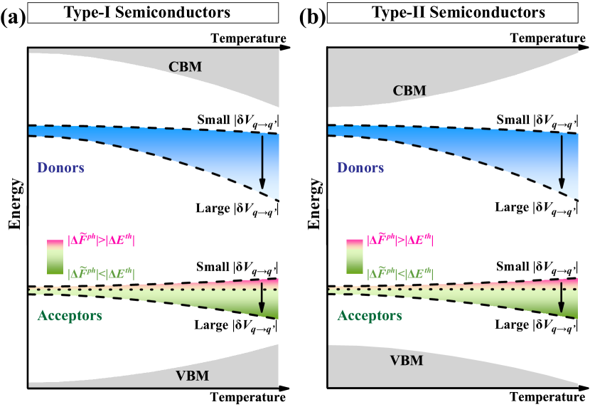
After having established the role of the free energy corrections, we next consider the changes in the band edge. Generally, there are two typical types of temperature-dependent band edge changes, as demonstrated in Fig. 1. In many conventional semiconductors, e.g., GaN 33 ; 34 and GaAs 35 , the CBM (VBM) energy positions usually downshift (upshift) as temperature increases, e.g., CBM<0 and VBM>0, denoted as type-I semiconductors (Fig. 1a). Type-II semiconductors (Fig.1b), e.g., CsPbI3 36 and MAPbI3 37 ; 38 , are opposite to the type-I cases, e.g., CBM>0 and VBM<0. Combining Rule I and specific band edge changes, we arrive at Rule II on the temperature dependence of rα(q/q’) in semiconductors. Rule II(a) for donors: the rα(q/q’) in type-I semiconductors can become shallower, deeper or stay unchanged under different temperatures (Fig. 1a), depending on the different strengths of the opposing effect between aα(q/q’) and CBM; the rα(q/q’) in type-II semiconductors will always become deeper (Fig. 1b), due to the synergistic effect between aα(q/q’) and CBM. Rule II(b) for acceptors: the rα(q/q’) with small (large) |V| in type-I (type-II) semiconductors can become either shallower, deeper or stay unchanged as a function of temperature, originating from the opposing effect between aα(q/q’) and VBM; the rα(q/q’) with large (small) |V| in type-I (type-II) semiconductors will always become shallower (deeper), due to the synergistic effect between aα(q/q’) and VBM, as shown in Fig. 1a (Fig. 1b).
C. Verification in GaN
Taking GaN as a prototype example, we have systematically studied the effects of temperature on α(q/q’) for ten different defects [see S.I in Supplementary Material (SM)]. The donor-like defects include N vacancy (VN), substitutional SiGa, GeGa, and ON, while the acceptor-like defects include MgGa, ZnGa, BeGa, CaGa, CdGa, and CN 39 ; 40 . Many of them are commonly observed in GaN 39 ; 40 .
First, we test the relationship between Fel and V in GaN. As shown in Fig. 2a, the calculated Fel and Eth for these defects are almost identical, except for SiGa and ON between 0 and +1 charge-state transitions at T>800 K, confirming that the contributions of Eel and Sel to Fel are usually small in semiconductors 12 ; 31 . Deviations at high temperatures partially originate from the shallow-level-induced electron-occupation changes. Eth can be directly evaluated using first-principles calculations under hydrostatic-stress conditions 42 ; 43 , adopting the experimental V 44 . As shown in Fig. 2a, the calculated Eth of these defects increase almost linearly as temperature increases. Interestingly, the calculated V are all positive (negative) for the acceptors (donors) during ionization, resulting in the negative (positive) Eth. Taking 800 K as a typical temperature, as shown in Fig. 2b, we have plotted the relationship between Eth and V for these defects, which exhibits an almost linear dependence, confirming our expectation from Eq. (3). A similar linear dependence behavior with different slopes is observed at other temperatures [Fig.S1 in S.II].
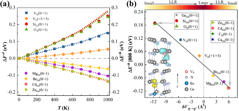
It is interesting to understand the origin of the diverse V values for different defects. Overall, we discover that while V is mainly determined by the change of LEO, the LLR can effectively compensate the LEO-induced |V|; the larger the LLR, the smaller the |V|. For example, as shown in Fig. 2b, all donors have a similar V0→+1-12 3 except VN. The V of VN are q/q’ dependent, e.g., V0→+1-6 3 and V+1→+3-1 3. Meanwhile, all the acceptors have similar V0→-1 +6 3 expect MgGa (+4.8 3) and BeGa (+2.3 3). Overall, V is mainly determined by the change of LEO around the defect, i.e., the increased (decreased) LEO always significantly increases (decreases) the local volume around a defect 45 , leading to a positive (negative) V. Furthermore, the V value also depends on the strength of LLR around the defect. For example, for SiGa, there is a negligible LLR during the ionization (Fig. S2 in S.II), therefore, the large V0→+1 -12 3 is mainly induced by the decreased LEO around SiGa. The cases of GeGa and ON are similar to that of SiGa, resulting in similar V0→+1 values. For VN, due to the broken ionic bonds around VN, the extra electrons from the dangling bonds (DBs) are strongly localized around VN (up-inset, Fig. 2b). During the ionization from 0 to +1, the DB electrons could be partially compensated, which consequently reduces electron screening and enhances Coulomb repulsion between the neighboring Ga+3 ions around VN. As a result, the large LLR effect around VN (Fig. S3 in S.II) effectively expands the local volume and partially compensates the initial local volume shrinkage induced by the decreased LEO. Therefore, the V0→+1 of VN is significantly smaller than that of SiGa. In a similar way, the V+1→+3 of VN can be further reduced from -6 to -1 3, due to the further enhanced LLR effect (Fig. S3 in S.II).
Similar to SiGa, a negligible LLR also exists in acceptors such as ZnGa, CN, CaGa and CdGa (Fig. S4 in S.II). As a result, the increased LEO gives rise to a large V0→-1 6 3 for these acceptors. However, for BeGa, the smaller atomic size of Be compared to Ga induces one broken ionic-bond around BeGa along the c direction, resulting in a DB hole on the broken N bond (bottom-inset, Fig. 2b) 46 . During the ionization, the DB hole is fully compensated, resulting in a strongly enhanced Coulomb attraction that restores the Be-N bond along the c direction and shrinks the local volume around BeGa (Fig. S5 in S.II). This large local volume shrinkage induced by the LLR effect largely compensate the initial local volume expansion induced by the increased LEO. Hence, compared to CdGa, the V0→-1 of BeGa is reduced to +2.3 3. The strength of LLR in MgGa (Fig. S6 in S.II) is between BeGa and CdGa, resulting in an intermediate V0→-1 value between that of BeGa and CdGa. Therefore, as shown in Fig. 2b, we conclude that the variable V in different defects are mainly determined by the competing effect between LEO and LLR.
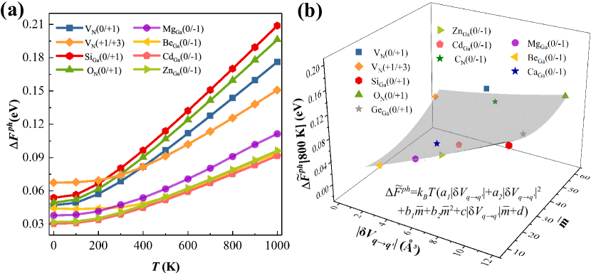
Second, we explore the relationship between Fph and V in GaN. As shown in Fig. 3a, the Fph of both donors and acceptors are positive and increase with increasing temperature. Here, we focus on the ph, which determines the temperature dependence of Fph. We expect that |V| and are the two main factors in determining ph. Indeed, the ph values of all the defects at different temperatures can be well fitted by a simple but unified formula given as
| ((5)) |
Fig. 3b shows the case of T=800 K. Similar behaviors are observed at other temperatures but with different parameter values (Fig.S7 in S.II). Overall, it is found that the |V| term is the dominant factor for ph, and a larger |V| usually gives a larger ph. For example, the larger ph of SiGa compared to CdGa (116 v.s. 44 meV) is mainly due to its larger |V| (12 v.s. 6 3). For defects with similar |V| values, becomes important in determining ph, and a smaller gives a larger ph. For example, comparing CaGa, ZnGa, and CdGa, which have a similar |V|6 3, CaGa with smaller (19.2) than ZnGa (24.2) and CdGa (33.6) has larger ph (80 meV) compared to ZnGa (47 meV) and CdGa (44 meV). We notice that the calculated ph value for CN at 600 K also agrees with a previous study 19 .
Combining the results of Fel (Fig. 2a) and Fph (Fig. 3a), we arrive at the temperature-dependent α(q/q’) of defects in GaN. GaN is a type-I semiconductor 33 , whose |CBM| (Fig. 4a) is noticeably larger than |VBM| (Fig. 4b) at a given temperature, due to the different band-edge orbital characters 33 ; 49 . Importantly, the calculated bandgap of GaN as a function of temperature agrees well with the experimental measurements 34 , confirming the reliability of our computational methods (Fig. S8 in S.II).
As shown in Fig. 4a, three typical donors, i.e., VN, SiGa, and ON, are selected to demonstrate the temperature dependence of α(q/q’) for donors, to verify our proposed Rules I(a) and II(a). Interestingly, these donors exhibit quite different temperature-dependent behaviors. Without the consideration of VBM, the aα(q/q’) of all the donors become deeper as the temperature increases, i.e., the higher the temperature, the deeper the aα(q/q’). Surprisingly, the aα(0/+1) of SiGa and VN, which have similar shallow levels at T=0 K (with the inclusion of Fzp contribution), exhibit dramatically different temperature dependences, i.e., the change of aα(0/+1) in SiGa (-0.44 eV) in the range 0<T<1000 K is much larger than that in VN (-0.28 eV), due to the significantly larger |V0→+1| in SiGa (Fig. 2b). Interestingly, although the aα(0/+1) of ON is much deeper than that of SiGa at 0 K, they exhibit almost the same trend of aα(0/+1) under different temperatures, due to their similar |V0→+1| (the slight difference at high temperatures is caused by their different ). Unexpectedly, the aα(q/q’) of one defect can also exhibit totally different behaviors under different charge-state transitions. For example, the aα(0/+1) and aα(+1/+3) for VN are dramatically different because of their largely different |V| (Fig. 2b). The above observations, along with other calculated donors (Fig. S9a in S.II), confirm the proposed Rule I(a) on the relationship between |V| and aα(q/q’) for donors at different temperatures.
Combining aα(q/q’) with the calculated CBM bowing of GaN, we obtain the rα(q/q’) of donors. Interestingly, as exhibited in Fig. 4c, the rα(q/q’) can become either shallower [rα(q/q’)>0], deeper [rα(q/q’)<0] or even unchanged [rα(q/q’)0] for different donors in different temperature regions. For examples, for SiGa and ON, rα(0/+1)0 in the range 0<T<500 K, due to the largest opposing effect between |CBM| and |aα(0/+1)| (|CBM||aα(0/+1)|); for T>500 K, |CBM|<|aα(0/+1)| gives rise to rα(0/+1)<0, e.g., rα(0/+1) of SiGa is -0.04 eV at T=1000 K. For VN, |CBM|> |aα(0/+1)| in the range 0<T<1000 K, resulting in rα(q/q’)>0. Among all the rα(q/q’), the largest value occurs in the rα(+1/+3) of VN (0.33 eV at T=1000 K), due to the smallest opposing effect between |CBM| and |aα(+1/+3)|. The above observations, along with other calculated donors (Fig. S9a in S.II), confirm our proposed Rule II(a) that the rα(q/q’) of donors in type-I semiconductors is determined by the relative magnitude and sign of aα(q/q’) and CBM.
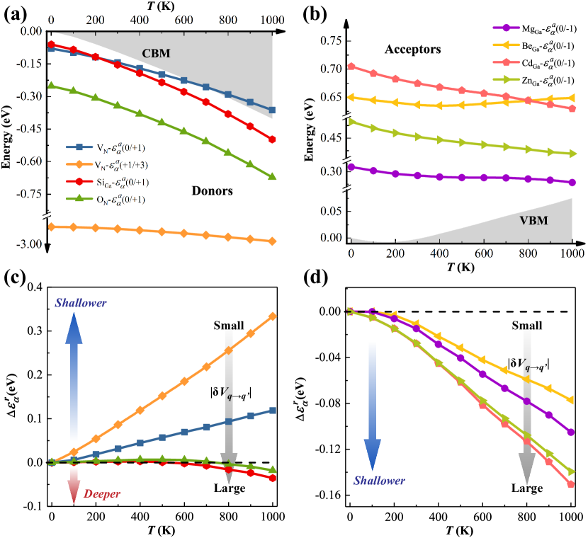
In Fig. 4b, four typical acceptors, i.e., ZnGa, MgGa, BeGa, and CdGa, are selected to demonstrate the temperature dependence of α(q/q’) for acceptors, to verify our proposed Rules I(b) and II(b). Holding large |V0→-1|, the aα(0/-1) of CdGa and ZnGa always becomes shallower [i.e., aα(0/-1)<0] as temperature increases. Interestingly, regardless of the significantly different aα(0/-1) values at 0 K for CdGa and ZnGa, their aα(0/-1) exhibit similar temperature dependences, mostly due to their similar |V0→-1| (Fig. 2b). Again, their slightly different aα(0/-1) at high temperatures could be due to their different . Surprisingly, although the CdGa and BeGa have close aα(0/-1) values at 0 K, their aα(0/-1) exhibit different (even opposite) temperature dependences, due to their significantly different |V0→-1| (Fig. 2b); with small |V0→-1|, the aα(0/-1) of BeGa becomes even deeper when T>400 K, swapping the relative positions of CdGa and BeGa at T=0 K and T=1000 K. Since the |V0→-1| of MgGa is in between CdGa and BeGa, the aα(0/-1) of MgGa is 0 in the range 300<T<700 K. These observations, along with other calculated acceptors (Fig. S9b in S.II), confirm the Rule I(b) on the aα(q/q’) of acceptors, especially the critical role played by |V|. We emphasize that the values of |aα(q/q’)| for acceptors are usually much smaller than those for donors, due to the large cancelling effect between Fel and Fph for acceptors.
Combining aα(q/q’) with the calculated VBM bowing of GaN, we can obtain the rα(q/q’) of acceptors. Overall, as shown in Fig. 4d, the rα(0/-1) of all acceptors in GaN becomes shallower [i.e., rα(0/-1)<0]. For CdGa and ZnGa, the synergistic effect between aα(0/-1) and VBM results in a large value of rα(0/-1), e.g., rα(0/-1)=-0.15 eV at T=1000 K. For MgGa with aα(0/-1)0, its rα(0/-1) closely follows the trend of VBM. For BeGa, the opposing effect between aα(0/-1) and VBM leads to a small rα(0/-1). The above observations, along with other calculated acceptors (Fig. S9b in S.II), confirm our proposed Rule II(b) that the rα(q/q’) of acceptors in type-I semiconductors, depending on the size of |V|, can exhibit either synergistic or opposing effects between aα(q/q’) and VBM.
III. Conclusion and Outlook
We emphasize that, although the overall sizes of |α(q/q’)| are not huge in GaN (generally <0.4 eV), we expect that the temperature effect, obeying the same rules as we have developed, could be much more noticeable in many other systems, e.g., superhard semiconductors (e.g., diamond, in which defects play a key role for realizing quantum bits) or organic-inorganic hybrid perovskites (e.g., MAPbI3, in which defects play a key role for limiting their solar efficiencies), in which the phonon vibrations or band edge changes are much more significant than those in GaN. Since the carrier concentrations and defect-mediated non-radiative carrier recombination in semiconductors are very sensitive to the positions of α(q/q’) inside the bandgap that are temperature dependent, our theory may also be applied to reexamine or explain many existing puzzles on the disagreements between experimental measurements and static first-principles calculations.
In conclusion, we have derived the basic formulas and consequently established two fundamental rules for the temperature dependence of α(q/q’) for both donors and acceptors in semiconductors, a question that has remained unanswered for decades. As we demonstrated in GaN, the temperature-driven changes of α(q/q’) for different defects can be rather diverse, i.e., it can become shallower, deeper or stay unchanged. The ultimate behavior is mainly determined by the synergistic or opposing effects between free energy corrections and band edge changes. In particular, we discover a previously ignored physical quantity, V, that plays an unexpectedly central role in determining the temperature evolution of α(q/q’). Generally, these basic formulas and fundamental rules may potentially be applied to design novel semiconductor devices operated under high or varying temperatures.
Acknowledgements
We thank Drs. J. B. Chen and P. Li for helpful discussions. S.-H.W. and B.H. acknowledge support from the NSFC (Grant Nos. 11634003, 12088101) and NSAF U1930402. S. Q. acknowledges support from the NSFC (Grant No. 12047508) and Chinese Postdoctoral Science Foundation (Grant No. 2021M690329). Y.-N.W. acknowledges support from the Program for Professor of Special Appointment (Eastern Scholar TP2019019). B.M. acknowledges support from the Gianna Angelopoulos Programme for Science, Technology, and Innovation and from the Winton Programme for the Physics of Sustainability. Part of the calculations were performed at Tianhe2-JK at Computational Science Research Center.
S.Q. and Y.-N.W. contributed equally to this work.
APPENDIX A: Derivation of α(/) at finite temperature
Without the inclusion of temperature effects, the formation energy of a defect in charge state q is defined as 12 ; 13 ; 50 :
| ((A1)) |
E(,q) is the total energy of the supercell with defect in charge state q, whereas E(host) is the total energy of perfect host without defect or impurity. E(i) is the energy of the elemental constituent i at its elemental monomeric phases, and i is its chemical potential refer to E(i). ni is the number of atoms exchanged with the external environment during the formation of defects for element i, and the charge state q is the number of electrons transferred from the supercell to the reservoirs. VBM(host) is the valence band maximum (VBM) of the host material and EF is the Fermi energy refer to VBM(host).
The α(q/q’) is the Fermi level at which the charge state q has the same formation energy with q’:
| ((A2)) |
With the inclusion of temperature effects, the H(,q) in Eq.(A1) is replaced by the Gibbs free energy G(,q), and the E(,q) [E(,q’)] is replaced by free energy F(,q) [F(,q’)]
| ((A3)) |
where P and T are the pressure and temperature, respectively. V and Vhost are the volumes of the system with defects and the host system under pressure P, respectively. In our case of no external pressure (P=0), Eq.(A3) can be written as
| ((A4)) |
Accordingly, with the inclusion of temperature effects, α(q/q’) is given by
| ((A5)) |
The free energy F can be expanded around the equilibrium position as
| ((A6)) |
where RI are the atomic coordinates of atom I, and RI0 are the equilibrium position. uk, defined as Rk-Rk0, are the atomic displacements of atom k from the equilibrium positions. The first and second terms are the electron and phonon free energies, respectively. Accordingly, F0 includes two parts, E (the total energy of the system without the consideration of temperature effects) and Fel (the corrections of the free energy induced by the electron contribution). Ignoring high order terms, we have
| ((A7)) |
where Fph is the correction of the free energy induced by the phonon vibration.
Under the quasi-harmonic approximation (QHA), Fel can be written as 13 ; 29 ; 30
| ((A8)) |
where the first, second, and third terms are the contributions from thermal expansion, electron-occupation change, and electronic entropy, respectively. Generally, the contributions of the Eel and Sel are negligible in semiconductors, as also verified in our calculations [Fig2(a)]. Therefore, we focus on the Eth term in Fel.
Under the QHA, Fph can be written as 32
| ((A9)) |
where the , i, and kB are the reduced Planck constant, phonon eigenfrequency, and Boltzmann constant, respectively.
Combining Eq.(A6) to Eq.(A9), we can obtain the α(q/q’) of defects under different temperatures
| ((A10)) |
The second term of Eq.(A10) represents the correction on the free energy differences between the q and q’ configurations induced by the electronic (Fel) and vibrational (Fph) contributions. The third term of Eq.(A10) represents the correction on the VBM energy position induced by thermal expansion and electron-phonon coupling (VBM = thVBM+phVBM).
Without consideration of the external pressure, volume expansion induced by rising temperature can be described by the thermal expansion coefficient. From the definition of mean volumetric thermal expansion coefficient, we can obtain that T and V are correlated by S24
| ((A11)) |
where V is the mean volumetric thermal expansion coefficient, and V0 is the equilibrium volume of the system at 0 K. Thus, in case of no external pressure, we can keep T as the only variable in our formula, and the α(q/q’) at a finite temperature becomes
| ((A12)) |
At a given temperature , Fel(Eth) and thVBM can be directly calculated via first-principles calculations under hydrostatic-stress conditions 42 ; 43 (it is noted that the lattice constant after thermal expansion is determined by the experiment thermal expansion coefficients of GaN S9 ), Fph can be determined through Eq.(A9) and the calculations of phonon eigenfrequencies for charge states q and q’. Finally, phVBM can be calculated using the finite displacement approach based on thermal lines S10 ; S11 . Unlike the conventional finite-displacement approach that evaluates each phonon separately and sum over all phonons, this stochastic approach considers all phonon modes at the same time, and the electron-phonon interaction can be calculated accurately and efficiently.
APPENDIX B: Derivation of Eth
Under the QHA, the thermal expansion induced energy correction Eth, can be treated as arising from strain 42 ; 43 . Therefore, the corrections on the total energy differences between the system with and without defect induced by the thermal expansion can be written as 45
| ((B1)) |
0 is the elastic constant of the host and is the change of 0 induced by a defect in charge state q. Vq=V0(,q)-V0(host) is the volume change induced by the defect at 0 K, in which V0(host) and V0(,q) are the equilibrium volume of the system without and with defect at 0K.
We assume that in a large system, a single defect cannot strongly influence the elastic constant, i.e., =0 as a first-order approximation, and Eth between the two charge states q and q’ with the same defect is
| ((B2)) |
where V=V0(,q’)-V0(,q) is the volume change induced by the defect at 0 K when the charge-state changes from q to q’. Combining Eq.(A11), we have
| ((B3)) |
APPENDIX C: Derivation of Fph
The phonon contribution to the free energy, Fph, can be described by Eq.(A9). Considering the first-order approximation of the Taylor expansion ex=1+x+x2/2!+x3/3!+…, we have
| ((C1)) |
The Fph between the two charge states q and q’ with the same defect is given by [two states with the same defect have the same number of phonon (i)]
| ((C2)) |
Defining i= i(,q’)-i(,q) and considering the first-order approximation of the Taylor expansion ln(1+x)=x-x2/2+x3/3-…, we have
| ((C3)) |
References
- (1) W. S. Yang, et al. Iodide management in formamidinium-lead-halide-based perovskite layers for efficient solar cells, Science 356, 1376 (2017).
- (2) J. Jeong, et al. Pseudo-halide anion engineering for -FAPbI3 perovskite solar cells, Nature 592, 381 (2021).
- (3) J. Kong, et al. CO2 doping of organic interlayers for perovskite solar cells, Nature 594, 51 (2021).
- (4) K. Lin, et al. Perovskite light-emitting diodes with external quantum efficiency exceeding 20 per cent, Nature 562, 245 (2018).
- (5) J. Luo, et al. Efficient and stable emission of warm-white light from lead-free halide double perovskites, Nature 563, 541 (2018).
- (6) S.-Y. Xu, et al. Topological Phase Transition and Texture Inversion in a Tunable Topological Insulator, Science 332, 560 (2011).
- (7) J. Zhang, et al. Topology-Driven Magnetic Quantum Phase Transition in Topological Insulators. Science 339, 1582 (2013).
- (8) J. L. Collins, et al. Electric-field-tuned topological phase transition in ultrathin Na3Bi, Nature 564, 390 (2018).
- (9) W. F. Koehl, B. B. Buckley, F. J. Heremans, G. Calusine, and D. D. Awschalom, Room temperature coherent control of defect spin qubits in silicon carbide, Nature 479, 84 (2011).
- (10) Y. He, et al. A two-qubit gate between phosphorus donor electrons in silicon, Nature 571, 371 (2019).
- (11) N. P. de Leon, et al. Materials challenges and opportunities for quantum computing hardware, Science 372, 253 (2021).
- (12) A. Alkauskas, et al. Advanced Calculations for Defects in Materials: Electronic Structure Methods, (John Wiley Sons, Weinheim, 2011).
- (13) C. Freysoldt, et al. First-principles calculations for point defects in solids, Rev. Mod. Phys. 86, 253 (2014).
- (14) A. Zunger, and O. I. Malyi, Understanding doping of quantum materials, Chem. Rev. 121, 3031 (2021).
- (15) K. Carling, et al. Vacancies in Metals: From First-Principles Calculations to Experimental Data, Phys. Rev. Lett. 85, 3862 (2000).
- (16) M. Youssef, and B. Yildiz, Intrinsic point-defect equilibria in tetragonal ZrO2: Density functional theory analysis with finite-temperature effects, Phys. Rev. B 86, 144109 (2012).
- (17) A. Glensk, B. Grabowski, T. Hickel, and J. Neugebauer, Breakdown of the Arrhenius Law in Describing Vacancy Formation Energies: The Importance of Local Anharmonicity Revealed by Ab initio Thermodynamics, Phys. Rev. X 4, 011018 (2014).
- (18) J. B. Casady, and R. W. Johnson, Status of Silicon Carbide (SiC) as a Wide-bandgap Semiconductor for High-temperature Applications: A Review, Solid-State Electron. 39, 1409 (1996).
- (19) P. G. Neudeck, R. S. Okojie, and L.-Y. Chen, High-Temperature Electronics-A Role for Wide Bandgap Semiconductors?, Proc. IEEE 90, 1065 (2002).
- (20) J. Milln, P. Godignon, X. Perpi, A. Prez-Toms, and J. Rebollo, A Survey of Wide Band Gap Power Semiconductor Devices, IEEE Trans. Power Electron. 29, 2155 (2014).
- (21) T. Harada, S. Ito, and A. Tsukazaki, Electric dipole effect in PdCoO2/-Ga2O3 Schottky diodes for high-temperature operation, Sci. Adv. 5, eaax5733 (2019).
- (22) X. Wang, et al. Radiation-induced segregation in a ceramic, Nat. Mater. 19, 992 (2020).
- (23) P. L. Dreike, D. M. Fleetwood, D. E. King, D. C. Sprauer, and T. E. Zipperian, An Overview of High-Temperature Electronic Device Technologies and Potential Applications, IEEE Trans. Comp., Packag., Manufact. Technol. A 17, 594 (1994).
- (24) D. G. Senesky, B. Jamshidi, K. B. Cheng, and A. P. Pisano, Harsh Environment Silicon Carbide Sensors for Health and Performance Monitoring of Aerospace Systems: A Review, IEEE Sensors J. 9, 1472 (2009).
- (25) T. Ghidini, Materials for space exploration and settlement, Nat. Mater. 17, 846 (2018).
- (26) O. Tschauner, et al. Ice-VII inclusions in diamonds: Evidence for aqueous fluid in Earth’s deep mantle, Science 359, 1136 (2018).
- (27) B. Monserrat, Electron-phonon coupling from finite differences, J. Phys.: Condens. Matter 30, 083001 (2018).
- (28) X. Yan, P. Li, S.-H. Wei, and B. Huang, Universal Theory and Basic Rules of Strain-Dependent Doping Behaviors in Semiconductors, Chin. Phys. Lett. 38, 087103 (2021).
- (29) N. D. Mermin, Thermal Properties of the Inhomogeneous Electron Gas, Phys. Rev. 137, A1441 (1965).
- (30) Y. Wang, Z. K. Liu, and L. Q. Chen, Thermodynamic properties of Al, Ni, NiAl, and Ni3Al from first-principles calculations, Acta Mater. 52, 2665 (2004).
- (31) S. Baroni, S. de Gironcoli, A. Dal Corso, and P. Giannozzi, Phonons and related crystal properties from density-functional perturbation theory, Rev. Mod. Phys. 73, 515 (2001).
- (32) D. C. Wallace, Thermodynamics of Crystals, (Dover, New York, 1998).
- (33) E. Zdanowicz, et al. As-related stability of the band gap temperature dependence in N-rich GaNAs, Appl. Phys. Lett. 115, 092106 (2019).
- (34) K. B. Nam, J. Li, J. Y. Lin, and H. X. Jiang, Optical properties of AlN and GaN in elevated temperatures, Appl. Phys. Lett. 85, 3489 (2004).
- (35) Y. P. Varshni, Temperature dependence of the energy gap in semiconductors, Physica 34, 149 (1967).
- (36) R. Saran, A. Heuer-Jungemann, A. G. Kanaras, and R. J. Curry, Giant Bandgap Renormalization and Exciton-Phonon Scattering in Perovskite Nanocrystals, Adv. Opt. Mater. 5, 1700231 (2017).
- (37) R. L. Milot, G. E. Eperon, H. J. Snaith, M. B. Johnston, and L. M. Herz, Temperature-Dependent Charge-Carrier Dynamics in CH3NH3PbI3 Perovskite Thin Films, Adv. Funct. Mater. 25, 6218 (2015).
- (38) M. Ibrahim Dar, et al. Origin of unusual bandgap shift and dual emission in organic-inorganic lead halide perovskites, Sci. Adv. 2, e1601156 (2016).
- (39) C. G. Van de Walle, and J. Neugebauer, First-principles calculations for defects and impurities: Applications to III-nitrides, J. Appl. Phys. 95, 3851 (2004).
- (40) M. A. Reshchikov, and H. Morkoç, Luminescence properties of defects in GaN, J. Appl. Phys. 97, 061301 (2005).
- (41) A. Togo, L. Chaput, I. Tanaka, and G. Hug, First-principles phonon calculations of thermal expansion in Ti3SiC2, Ti3AlC2, and Ti3GeC2, Phys. Rev. B 81, 174301 (2010).
- (42) A. Togo, and I. Tanaka, First principles phonon calculations in materials science, Scripta Mater. 108, 1 (2015).
- (43) H. P. Maruska, and J. J. Tietjen, The Preparation and Properties of Vapor-Deposited Single-Crystalline GaN, Appl. Phys. Lett. 15, 327 (1969).
- (44) S. Lany, and A. Zunger, Dual nature of acceptors in GaN and ZnO: The curious case of the shallow MgGa deep state, Appl. Phys. Lett. 96, 142114 (2010).
- (45) D. Wickramaratne, et al. Defect identification based on first-principles calculations for deep level transient spectroscopy, Appl. Phys. Lett. 113, 192106 (2018).
- (46) Y.-H. Li, X. G. Gong, and S.-H. Wei, Ab initio all-electron calculation of absolute volume deformation potentials of IV-IV, III-V, and II-VI semiconductors: The chemical trends, Phys. Rev. B 73, 245206 (2006).
- (47) T. J. Ahrens, Mineral Physics & Crystallography: A Handbook of Physical Constants, (American Geophysical Union, Washington, 1995).
- (48) H. P. Maruska, & J. J. Tietjen, The Preparation and Properties of Vapor-Deposited Single-Crystalline GaN, Appl. Phys. Lett. 15, 327 (1969).
- (49) B. Monserrat, Vibrational averages along thermal lines, Phys. Rev. B 93, 014302 (2016).
- (50) B. Monserrat, Correlation effects on electron-phonon coupling in semiconductors: Many-body theory along thermal lines, Phys. Rev. B 93, 100301(R) (2016).