Two-dimensional antiferromagnetic semiconductor T’-MoTeI from first principles
Abstract
Two-dimensional intrinsic antiferromagnetic semiconductors are expected to stand out in the spintronic field. The present work finds the monolayer T’-MoTeI is intrinsically an antiferromagnetic semiconductor by using first-principles calculation. Firstly, the dimerized distortion of the Mo atoms causes T’-MoTeI to have dynamic stability, which is different from the small imaginary frequency in the phonon spectrum of T-MoTeI. Secondly, T’-MoTeI is an indirect-bandgap semiconductor with 1.35 eV. Finally, in the systematic study of strain effects, there are significant changes in the electronic structure as well as the bandgap, but the antiferromagnetic ground state is not affected. Monte Carlo simulations predict that the Néel temperature of T’-MoTeI is 95 K. The results suggest that the monolayer T’-MoTeI can be a potential candidate for spintronics applications.
I INTRODUCTION
Since the initial rush of research on graphene, two-dimensional (2D) materials have drawn wide attention due to their novel physical properties KSNovoselov2004 ; KSNovoselov2005 ; AHCastroNeto2009 ; YMa2012 ; SLebegue2009 . Magnetically-ordered 2D crystals have brought infinite possibilities to development of new devices and discovery of physical phenomena. 2D magnetic semiconductors are of great potential for applications in low-dimensional spintronic devices because of their magnetic and semiconducting properties MAshton2009 ; LZhou2015 . Many 2D magnetic materials have been predicted so far, and some have been successfully prepared in experiments LDebbichi2016 ; HLiu2014 ; GRahman2017 ; VNicolosi2013 ; TJWilliams2015 . Because antiferromagnetic (AFM) semiconductors have stability under magnetic-field perturbations and large magneto-transport effects, 2D AFM semiconductors boast tremendous advantages in carrier injection, detection, sensors, and magnetic storage CGong2019 , but only a few 2D AFM semiconductors, such as Fe2Cl3I3, FePS3, and CoS2, have been reported so far LLiu2018 ; SChabungbam2017 ; YZhang2017 ; XXu2020 ; FKargar2020 ; ZZhang2020 . Further research on 2D intrinsic AFM semiconductors is necessary to promote practical applications.
In analysis of physical properties and applications of 2D materials, controlling the material structure is an effective method since two polymorphic structures may demonstrate drastically different properties despite the same chemical formula MKan2014 . For instance, layered MoS2, a famous transition-metal dichalcogenide (TMDC), has been extensively studied because of its distinctive electronic, optical, and mechanical properties QHWang2012 . Monolayer MoS2 has three common structures, namely H-MoS2, T-MoS2 and T’-MoS2 MAPy1983 ; FWypych1998 ; CAtaca2012 ; EBenavente2002 . H- and T-MoS2 structures are semiconductor and metal, respectively. An electron crystallography study observed on the surface of restacked MoS2 a new superstructure characterized by the formation of zigzag chains, which is called the distorted tetragonal MoS2 (T’-MoS2) YHLee2012 ; ASingh2015 ; SNShirodkar2014 ; XRQin1991 ; MHWhangbo1992 . In addition to extensive research on pure TMDCs, recent advances in experimental techniques have allowed researchers to combine properties of different TMDCs in a single polar material, namely the Janus structure. The top layer of the monolayer MoTe2 has been experimentally replaced by S atoms, namely MoSTe HJin2018 ; ZWang2018 . Compared with the H-MoSTe structure, T’-MoSTe exhibits more Raman-active modes (a total of 15 modes). The T’-MoSTe structure makes the Mo-Mo bonds shorter and thus significantly enhances the in-plane stiffness. This structure turns into a piezoelectric material when out-of-plane symmetry is broken MYagmurcukardes2019 . The obtainment of this monolayer compound has inspired many researchers to find a way to tune the physical properties of monolayer TMDCs. Synthesis of many polymorphic structures has been possible with the advancements of experimental techniques THu2018 .
If a halogen element with more electrons is introduced into pure TMDCs to form a Janus structure, it will affect the occupation of electrons in the Mo-d orbital, resulting in magnetism regulated by structural distortion and strains. In the present work, it is found that the monolayer T’-MoTeI is an antiferromagnetic semiconductor. After dimerized distortion, T’-MoTeI is observed and characterized by the formation of zigzag chains. The formation energy of T’-MoTeI is lower than that of T-MoTeI. The calculated phonon spectrum of T’-MoTeI without imaginary frequency shows the dynamic stability of T’-MoTeI. In addition, the projected band structure is obtained to analyze the composition near the Fermi level. The properties of antiferromagnetic semiconductors are stable under biaxial strains, but the band gap value changes. Furthermore, we found that strain-free T’-MoTeI exhibits a TN at 95 K, which can be improved to 210 K by the appropriate strain condition.
II METHODS OF COMPUTATIONAL
First-principles calculations were performed based on the density functional theory (DFT) WKohn1965 ; PHohenberg1964 with the projector-augmented wave (PAW) GKresse1995 method in the Vienna ab-initio Simulation Package (VASP) GKresse1993 ; GKresse1996 ; JFurthmller1996 . The structural optimization and convergence tests were adopted with the Perdew-Burke-Ernzerhof (PBE) JPPerdew1996 functional, and the electronic structures were given by the Heyd-Scuseria-Ernzerhof (HSE06) functional TBjrkmanl2011 . The force and total energy convergence criteria were set at 0.1 meV/Å and 10-8 eV for all the calculations. The plane-wave cutoff energy, width of smearing, number of k points in reciprocal space were set to 550 eV, 0.05 eV, , respectively. A 20Å vacuum layer was applied between two nearest slabs to avoid the interlayer interactions. The supercell was applied to perform phonon calculations ATogo2008 . In order to study the magnetic coupling between the magnetic moments on Mo atoms, we chose a supercell of in T’-MoTeI structure.
III RESULTS and DISCUSSION
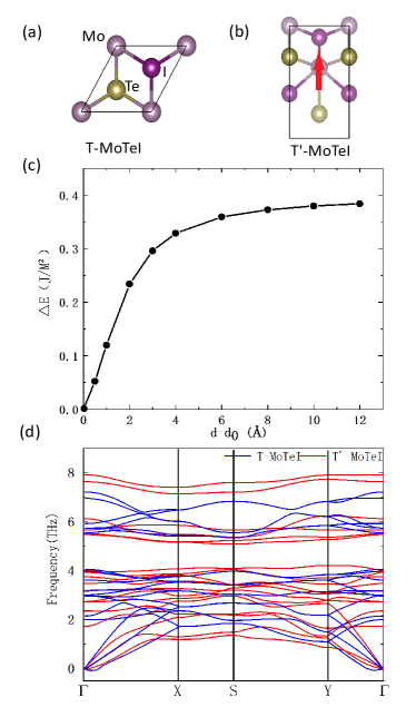
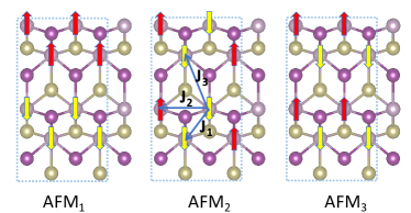
In the T-MoTeI structure, the Mo atoms are octahedral coordinated with the nearby three Te and I atoms, resulting in ABC stacking with P3m1 space group symmetry [Fig. 1(a)]. The equilibrium lattice constant is 3.9Å after high-precision structural optimization. After the triangular lattice was changed into a rectangular primitive cell and the Mo atom was moved away from its original position, T’-MoTeI, as a new structure, was observed and characterized by the formation of zigzag chains as the same as that in T’-TMDCs [Fig. 1(b)]. T’-MoTeI is a charge density wave state as a result of the Piers phase transition from T phase GEda2012 ; YGuo2015 ; GGao2015 . In order to identify their preferred magnetic ground state, a ferromagnetic (FM) and three antiferromagnetic (AFM) configurations were constructed (see Appendix). And the ground state is AFM2 configuration, when FM and NM energies are much larger than three AFM states.
Comparison of energy of different magnetic configurations shows that AFM2 is the most stable (see Appendix) and the magnetic moments are mostly localized on the magnetic centers of Mo (0.8 ) atoms, much more than those on Te (0.01 ) or I (0.01 ) atoms. It is worth noting that the ground state energy of T’-MoTeI is 1.98 eV, which is lower than that of T-MoTeI, and the following work mainly studies the ground state AFM2 of T’-MoTeI. Then, we estimate the ease of exfoliation by the so-called cleavage energy, which is defined as the energy required to separate the crystal into two halves along the gap between two T’-MoTeI layers. As shown in [Fig. 1(c)], the cleavage energy of T’-MoTeI is 0.37 J/m2, close to those in other 2D materials, which indicates the feasibility of experimentally preparing T’-MoTeI. The phonon spectra also show that the distortion of dimerization makes T’-MoTeI dynamically stable, which is different from the T-MoTeI which has imaginary phonon frequencies [Fig. 1(d)].
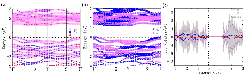
The spin projected band structure of monolayer T’-MoTeI are shown in [Fig. 2(a)]. The conduction band minimum (CBM) is located between Y and X points. The valence band maximum (VBM) is located between and X points. An indirect band gap of 1.35 eV is formed between CBM and VBM, smaller than the bandgap of T-MoTeI (1.80 eV), and indicates the intrinsic antiferromagnetic semiconductor of T’-MoTeI. The projected band structures and density of states (DOS) also shows that VBM and CBM are mainly contributed by Mo atoms when the contribution of Te-p and I-p orbitals are small around the bandgap [Fig. 2(b)]. Due to the distorted octahedral [Mo1Te3I3] of T’ structure, the Mo-d orbitals are roughly divided into upper eg (d, d) and lower t2g (dxy, dxz, dyz) orbitals by the crystal-field effect. In both VBM and CBM, t2g contributes more energy than eg. However, due to the influence of distortion, the eg and t2g orbitals are non-degenerate. Such a distortion further splits the d orbitals into five subgroups, as revealed by the orbital-resolved band structures. The orbitals are sequenced as follows by energy from low to high: dxy, dxz, dyz, d, and d. Thus, for Mo3+ in T’-MoTeI, there are three d electrons: two electrons completely fill the lowest dxy orbital, one electron half-occupies the dxz orbital. This results in one local magnetic moment for one Mo atom in T’-MoTeI.
Due to the different behaviors of dMo-Mo and dMo-Te under the strains, the mechanism of the AFM ground state and the strain effect on the magnetism can be understood by the competition between two different exchange interactions. On the one hand, the electrons occupying the t2g level have direct interaction between the nearest neighbor Mo atoms, which leads to the AFM arrangement. On the other hand, according to the Goodenough-Kanamori-Anderson (GKA) rules JKanamori1959 ; JBGoodenough1995 , Mo-Te-Mo bond angle of 69∘ in T’-MoTeI is smaller than 80∘, the indirect interaction of the compound contributes to AFM SLebernegg2013 ; ShijingZhang2009 . Further calculation shows that both negative direct and indirect interactions prove the AFM ground state of T’-MoteI.
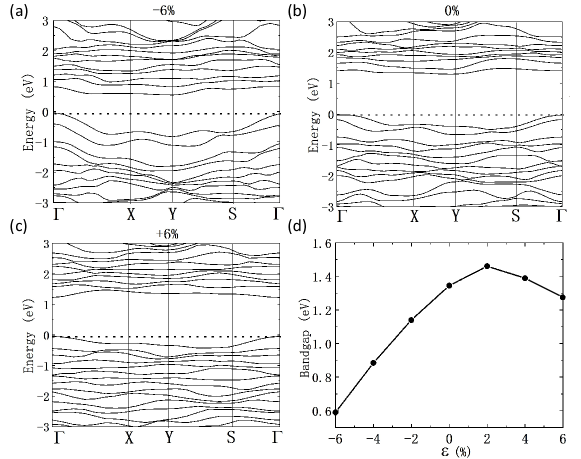
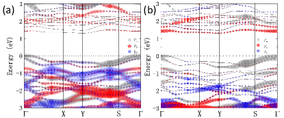
To explore the magnetic phase transitions in T-MoTeI and T’-MoTeI monolayers, a series of in-plane biaxial strains are applied. The value of strains applied are described by the change of the lattice parameter , where () and () are the lattice constants of unstrained and strained monolayer T’-MoTeI, respectively. The negative value denotes compressive strains and the positive value for tensile strains, and the range of strain is from -6% to 6%. As shown in [Fig. 3(a)], under a compressive strain of -6%, the CBM locates at Y-point and VBM locates at -point. While, both CBM and VBM at -point form a direct band gap under a tensile strain of 6% as shown in [Fig. 3(c)]. The band gap of T’-MoTeI can be tuned by as much as 50% by applying strains [Fig. 3(d)]. Under tensile strains, the bandgap rises to the maximum at a 2% strain and then decreases. For compressive strains, the bandgap decreases sharply.
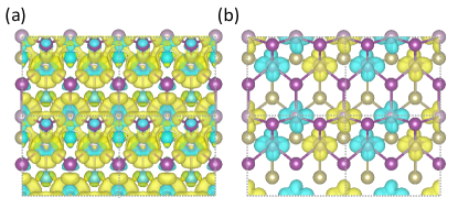
[Fig. 4(a)] shows the differential charge density of monolayer T’-MoTeI. It is defined as the difference between the charge density at the bonding point and the atomic charge density at the corresponding point. The yellow and blue regions represent charge accumulation and charge depletion, respectively. Significant charge redistributions are observed in Mo, Te and I atoms, where the Mo atoms lose electrons, while Te and I atoms gain electrons. This proves that the Mo element shows positive valence, but Te and I elements show negative valence. The spin densities for T’-MoTeI are shown in [Fig. 4(b)], where it can be observed that the spin-polarization mainly comes from Mo atoms, while the Te and I atoms are very small, which is consistent with the result of magnetic moment analysis.
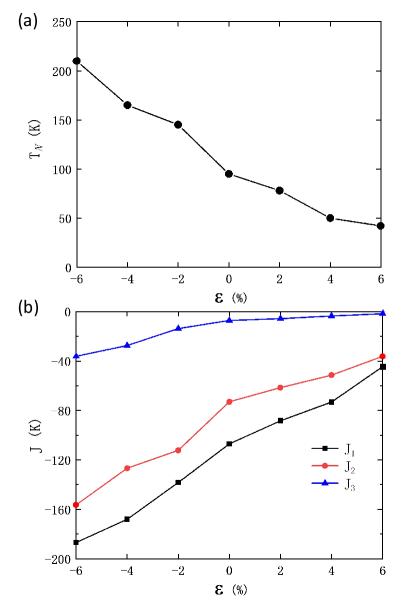
The Néel temperature (TN) is a key parameter in applications of AFM materials to spintronic devices. To explore the mechanism of magnetic phase transition, it is necessary to understand changes in magnetism with the temperature. We use the Ising model to characterize the magnetic coupling in monolayer T’-MoTeI. TN under different strains can be estimated by using MC simulations, as shown in [Fig. 5(a)]. The model Hamiltonian is written as
| (1) |
where Jij represents the exchange interactions of overall neighbor Mo-Mo pairs. Here we only consider the interaction between the nearest neighbor Mo atom (J1), the next nearest neighbor Mo atom (J2) and the third nearest neighbor Mo atom (J3), respectively. In order to calculate the exchange interactions, the total energy of monolayer T’-MoTeI with FM, AFM1, AFM2 and AFM3 configurations (see the Appendix) can be regard as
| (2) |
| (3) |
| (4) |
| (5) |
where represents the energy of nonmagnetic T’-MoTeI monolayer. MC simulations reveal that monolayer strain-free T’-MoTeI has a critical temperature about 95 K. The strain-dependent TN mainly originated from the obvious strain effect on the exchange interactions. As shown in [Fig. 5(b)], the J1, J2 and J3 changes monotonously with strain. According to the above equations about total energy, since J1, J2 and J3 are both negative, the strain-free ground state is the magnetic configuration of AFM2. It is found that the dMo-Mo changes from 2.8Å to 3.3Å between -6% and +6% phase transition, while dMo-Te is almost unchanged. This indicates that the changes of AFM strength in strains mainly come from the direct interaction between Mo atoms. Under the compressive strains, significantly reduced distance between the Mo atoms enhances the direct exchange interaction. For the considered largest compressive strain (= -6%), the J1 and TN values were -16 meV and 210 K, respectively. While, with the increase of dMo-Mo under the tensile strain, the corresponding J, and TN values decrease because of the weakened direct exchange interaction.
In conclusion, we studied the magnetic and electronic properties of T’-MoTeI monolayer using first-principles calculations. The phonon calculation indicates the structural stability of T’-MoTeI. Further studies on differential magnetic configurations and the critical temperature reveal that the monolayer T’-MoTeI has a Néel temperature above 95 K under strain-free condition. The present work also revealed the obvious impact of strains on the magnetic and electronic properties of T’-MoTeI. Our results show that the monolayer T’-MoTeI, as a new two-dimensional ferromagnetic semiconductor, will have great potential for nanoscale spintronic applications.
Acknowledgements.
This work is supported by National Natural Science Foundation of China (No. 11904312 and 11904313), and the Natural Science Foundation of Hebei Province of China (No. A2020203027).*
Appendix A A
References
- (1) K. S. Novoselov, A. K. Geim, S. V. Morozov, D. Jiang, Y. Zhang, S. V. Dubonos, I. V. Grigorieva, and A. A. Firsov, Science 306, 666 (2004).
- (2) K. S. Novoselov, A. K. Geim, S. V. Morozov, D. Jiang, M. I. Katsnelson, I. V. Grigorieva, S. V. Dubonos, and A. A. Firsov, Nature 438, 197 (2005).
- (3) A.H. Castro Neto, F. Guinea, N.M.R. Peres, K.S. Novoselov, and A.K. Geim, Rev. Mod. Phys. 81, 109 (2009).
- (4) Y. Ma, Y. Dai, M. Guo, C. Niu, Y. Zhu, and B. Huang, ACS Nano. 6, 1695 (2012).
- (5) S. Lebegue and O. Eriksson, Phys. Rev. B 79, 115409 (2009).
- (6) M. Ashton, J. Paul, S. B. Sinnott, and R. G. Hennig, Phys. Rev. Lett. 118, 106101 (2017).
- (7) L. Zhou, L. Kou, Y. Sun, C. Felser, F. Hu, G. Shan, S. C. Smith, B. Yan, and T. Frauenheim, Nano Letters 15, 7867 (2015).
- (8) L. Debbichi, H. Kim, T. Bjorkman, O. Eriksson, and S. Lebegue, Phys. Rev. B 93, 245307 (2016).
- (9) H. Liu, A. T. Neal, Z. Zhu, Z. Luo, X. Xu, D. Tomnek, and P. D, ACS Nano 8, 4033 (2014).
- (10) G. Rahman, A. U. Rahman, S. Kanwal, and P. Kratzer, EPL (Europhysics Letters) 119, 57002 (2017).
- (11) V. Nicolosi, M. Chhowalla, M. G. Kanatzidis, M. S. Strano, and J. N. Coleman, Science 340, 1226419 (2013).
- (12) T. J. Williams, A. A. Aczel, M. D. Lumsden, S. E. Nagler, M. B. Stone, J.-Q. Yan, and D. Mandrus, Phys. Rev. B 92, 144404 (2015).
- (13) C. Gong and X. Zhang, Science 363, 4450 (2019).
- (14) L. Liu, I. Kankam, and H. L. Zhuang, Phys. Rev. B 98, 205425 (2018).
- (15) S. Chabungbam and P. Sen, Phys. Rev. B 96, 045404 (2017).
- (16) Y. Zhang, L. Lin, J. J. Zhang, E. Dagotto, and S. Dong, Phys. Rev. B 95, 115154 (2017).
- (17) X. Xu, Y. Ma, T. Zhang, C. Lei, B. Huang, and Y. Dai, Nanoscale Horiz. 5, 1386 (2020).
- (18) F. Kargar, E. A. Coleman, S. Ghosh, J. Lee, M. J. Gomez, Y. Liu, A. S. Magana, Z. Barani, A. Mohammadzadeh, B. Debnath, R. B. Wilson, R. K. Lake, and A. A. Balandin, ACS Nano 14, 2424 (2020)
- (19) Z. Zhang, J. Y. You, B. Gu, and G. Su, The Journal of Physical Chemistry C 124, 19219 (2020).
- (20) M. Kan, J. Y. Wang, X. W. Li, S. H. Zhang, Y. W. Li, Y. Kawazoe, Q. Sun, and P. Jena, The Journal of Physical Chemistry C 118, 1515 (2014)
- (21) Q. H. Wang, K. Kalantar-Zadeh, A. Kis, J. N. Coleman, and M. S. Strano, Nature nanotechnology 7, 699 (2012).
- (22) M. A. Py and R. R. Haering, Canadian Journal of Physics 61, 76 (1983)
- (23) F. Wypych, T. Weber, and R. Prins, Chemistry of Materials 10, 723 (1998)
- (24) C. Ataca, H. ahin, and S. Ciraci, The Journal of Physical Chemistry C 116, 8983 (2012)
- (25) E. Benavente, M. Santa Ana, F. Mendizbal, and G. Gonzlez, Coordination Chemistry Reviews 224, 87 (2002).
- (26) Y.-H. Lee, X.-Q. Zhang, W. Zhang, M.-T. Chang, C.-T. Lin, K.-D. Chang, Y.-C. Yu, J. T.-W. Wang, C.-S. Chang, L.-J. Li, and T.-W. Lin, Advanced Materials 24, 2320 (2012)
- (27) A. Singh, S. N. Shirodkar, and U. V. Waghmare, 2D Materials 2, 035013 (2015).
- (28) S. N. Shirodkar and U. V. Waghmare, Phys. Rev. Lett. 112, 157601 (2014).
- (29) X. R. Qin, D. Yang, R. F. Frindt, and J. C. Irwin, Phys. Rev. B 44, 3490 (1991).
- (30) M. H. Whangbo and E. Canadell, Journal of the American Chemical Society 114, 9587 (1992)
- (31) H. Jin, T. Wang, Z.-R. Gong, C. Long, and Y. Dai, Nanoscale 10, 19310 (2018).
- (32) Z. Wang, J. Mater, Chem. C 6, 13000 (2018).
- (33) M. Yagmurcukardes, C. Sevik, and F. M. Peeters, Phys.Rev. B 100, 045415 (2019).
- (34) T. Hu, F. Jia, G. Zhao, J. Wu, A. Stroppa, and W. Ren, Phys. Rev. B 97, 235404 (2018).
- (35) W. Kohn and L. J. Sham, Phys. Rev. 140, 1133 (1965).
- (36) P. Hohenberg and W. Kohn, Phys. Rev. 136, 864 (1964).
- (37) G. Kresse, Journal of Non-Crystalline Solids 192, 222 (1995).
- (38) G. Kresse and J. Hafner, Phys. Rev. B 47, 558 (1993).
- (39) G. Kresse and J. Furthmller, Comput. Mater. Sci. 6, 0927 (1996).
- (40) G. Kresse and J. Furthmller, Phys. Rev. B 54, 11169 (1996).
- (41) J. P. Perdew, K. Burke, and M. Ernzerhof, Phys. Rev. Lett. 77, (1996).
- (42) T. Bjrkman, Computer Physics Communications 182, 1183 (2011).
- (43) A. Togo, F. Oba, and I. Tanaka, Phys. Rev. B 78, 134106 (2008).
- (44) G. Eda, T. Fujita, H. Yamaguchi, D. Voiry, M. Chen, and M. Chhowalla, ACS Nano 6, 7311 (2012).
- (45) Y. Guo, D. Sun, B. Ouyang, A. Raja, J. Song, T. F. Heinz, and L. E. Brus, Nano Letters 15, 5081 (2015).
- (46) G. Gao, Y. Jiao, F. Ma, Y. Jiao, E. Waclawik, and A. Du, The Journal of Physical Chemistry C 119, 13124 (2015).
- (47) J. Kanamori, J. Phys. Chem. Solids 10, 87 (1959).
- (48) J. B. Goodenough, Phys. Rev. 100, 564 (1955).
- (49) S. Lebernegg, M. Schmitt, A. A. Tsirlin, O. Janson, and H. Rosner, Phys. Rev. B 87, 155111 (2013).
- (50) Shijing Zhang, Guanghua Li, Jia Hua and so on, Chemical Journal of Chinese Universities 30, 227 (2009).