Spin Wave Propagation through Antiferromagnet/Ferromagnet Interface
Abstract
We study the problem of controlling spin waves propagation through an antiferromagnet/ferromagnet interface via tuning material parameters. It is done by introducing the degree of sublattice noncompensation of antiferromagnet (DSNA), which is a physical characteristic of finite-thickness interfaces. The DSNA value can be varied by designing interfaces with a particular disorder or curvilinear geometry. We describe a spin-wave propagation through any designed antiferromagnet/ferromagnet interface considering a variable DSNA and appropriate boundary conditions. As a result, we calculate the physical transmittance and reflectance of the spin waves as a function of frequency and show how to control them via the exchange parameters tuning.
Antiferromagnets (AFMs) are attractive as active elements for next-generation spintronic devices [1, 2, 3, 4]. The disadvantage of the last generation of spin-wave (SW) devices is their relatively low operating frequency, which is limited by the GHz range [5, 6, 7, 8, 9]. However, recent trends involving AFMs allow to raise this frequency to THz to successfully compete with optical devices [10, 11, 12, 13], because a spin manipulation in AFMs is inherently faster than in ferromagnets (FM) [14, 15]. The ultrafast generation, detection, and gate tuning of spin waves in AFMs are now becoming more and more accessible [15, 16], meanwhile the detection techniques in FMs are still better established [17, 18, 19].
The benefits of using AFMs have been recently actively studied [20, 21, 22, 23, 24, 25, 26, 27, 28]. Usually, AFMs are considered in limiting cases, namely, compensated, when the AFM has no static magnetization at the interface [29], and noncompensated, when the boundary of the AFM is magnetized [30]. AFMs with the fully compensated spin moments have implementations in terahertz range [31, 32, 33], e.g., spin-current driven AFM nano-oscillators have been proposed [34, 35]. On the other hand, the mechanisms of the AFM domain switching by current pulses [36, 37, 38] in certain cases are based on the electric field or spin torques acting on the noncompensated spins at the AFM interface [39, 40]. However, in some problems such as transmission of the spin current through a thin AFM insulator by means of evanescent AFM SWs, it has been recently assumed that the AFM could be partially noncompensated at the interface [41]. Moreover, it has been pointed out that the effective magnetic moment can be a complex arrangement of not fully compensated moments along compensated AFM structures [42]. Considering the compensated or noncompensated limiting cases significantly simplifies the description of underlying AFM physics, but does not cover the entire spectrum of the AFMs, and furthermore, requires perfectly flat AFM interfaces. Meanwhile, realistic rough interfaces with a variable degree of sublattice noncompensation are more common and therefore important to study.
In this paper, we investigate the SWs propagation through AFM/FM interface of a complex geometry. This problem can be solved by introducing an averaged characteristic of this interface – degree of sublattice noncompensation of AFM (DSNA). Due to strong exchange interactions between the AFM sublattices and with a neighboring material, this concept may play a crucial role in describing complex AFM interfaces with other magnetic media, i.e., those with a specific disorder or of curvilinear geometry. Complex interfaces with variable DSNA can be manufactured in a variety of ways, such as by engineering a particular surface roughness, ion implantation, vapor deposition or introduction of other defects [43, 44, 45, 46, 47].
We develop an analytical approach to a SW propagation from AFM to FM through any designed AFM/FM interface described by a variable DSNA. We consider the scattering of exchange SWs at the AFM/FM interface of finite thickness sandwiched between AFM and FM. We obtain the complete relations between the phases and amplitudes of scattered SWs taking into account the Poynting vector continuity at the boundary. This theory is designed for an exchange dominated regime, in which we derive the interface boundary conditions in the vicinity of noncompensated case, i.e., the DSNA . This case is of high interest as it gives rise to the largest exchange bias in AFM/FM structures.As a result, the frequency dependences of SW transmittance and reflectance at the interface are found in case.
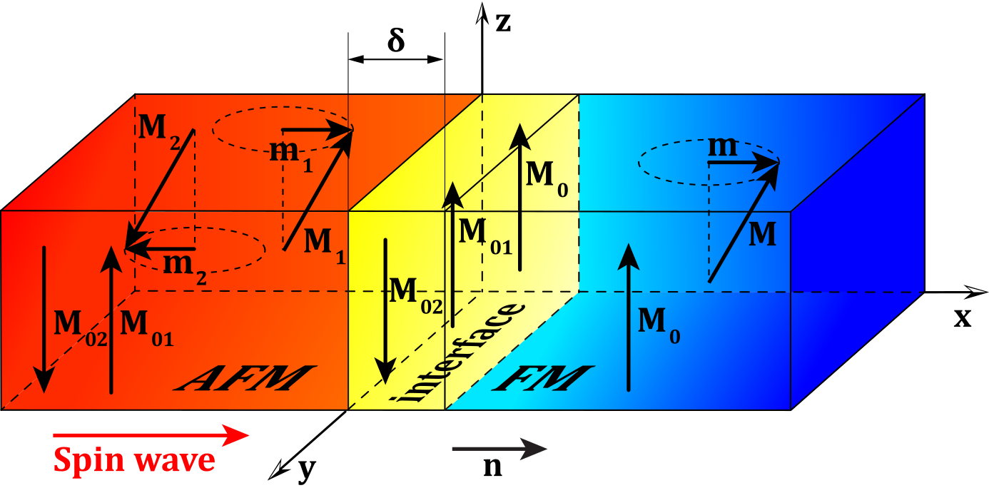
Model. We consider a one-dimensional scenario of SW propagation through an AFM/FM interface (along the -axis) as shown in Fig. 1. The interface has thickness and is parallel to the - plane. Since AFM has two sublattices and FM has one, we introduce three static (ground state) magnetizations within the interface and its surroundings, , , and , respectively. The media are magnetized by a strong enough uniform external magnetic field along the -axis, so all ground state magnetizations are (anti)parallel to the -axis. The small deviations of the magnetizations and from the ground state are introduced in the form and , where and are the dynamical components of the magnetization for the two AFM sublattices and FM, respectively, i.e., and .
To present the analytical theory of the SW propagation through the AFM/FM interface in an exchange dominated regime, only the exchange interactions between AFM and FM have to be taken into account within the interface [48, 49, 50]. We describe the magnetization dynamics by the Landau-Lifshitz (LL) equation 111The dissipation generally decreases the amplitudes of SWs, but does not influence their behavior qualitatively. Therefore, in the following we can use the LL equation approximation, where the dissipation is neglected., , where is the gyromagnetic ratio and is the effective magnetic field in each material. Here is the interfacial magnetic energy, and labels represent the two AFM sublattices and the one of FM. Integrating over the interface one finds the energy with being the cross-sectional area and the energy density at the interface :
| (1) | |||||
Here is the homogeneous AFM exchange parameter, is the exchange coupling parameter of each AFM sublattice with the FM, is the inhomogeneous FM exchange parameter, is the inhomogeneous exchange self-interaction parameter for each AFM sublattice, and is the inhomogeneous exchange interaction parameter between the AFM sublattices ( with and being the exchange stiffness constants [52]). Parameter can be estimated by , where is the lattice constant of the AFM [53, 52, 54]. The interactions in Eq. (1) include the antiferromagnetic coupling between two sublattices, the two couplings between each AFM sublattice and the FM [31], the exchange stiffness interaction of FM, the exchange self-interaction of the AFM sublattices, and the exchange interaction between AFM sublattices, respectively.
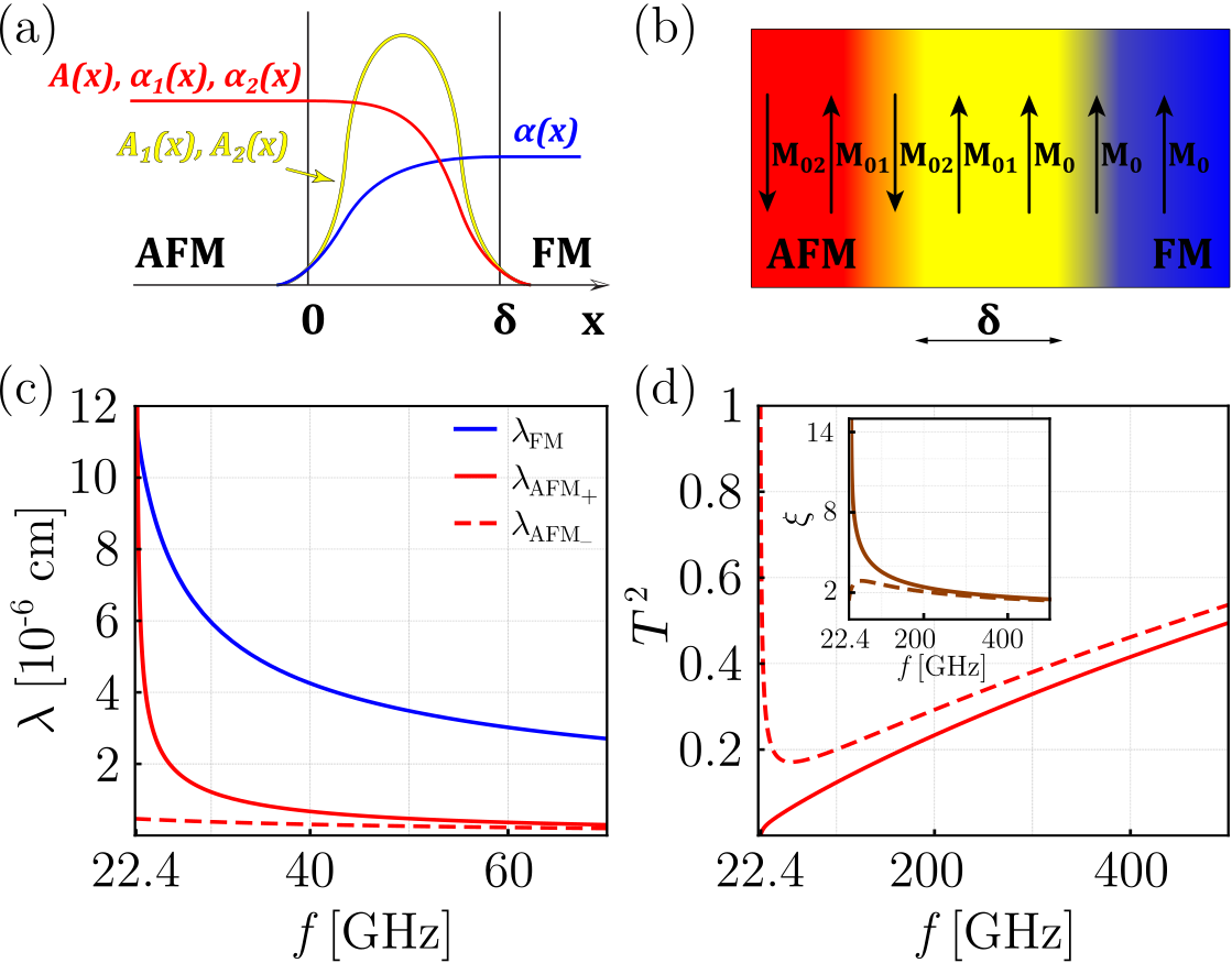
AFM/FM boundary conditions. To derive the interfacial boundary conditions, order parameters , and are considered as slowly varying functions, whereas the coefficients , , , , , and are varying significantly within the interface as shown in Fig. 2 (a). We define the interface in terms of the averaged properties of the surrounding materials, so the LL equations are integrated over the thickness of the interface [55, 48, 56, 57]. Then at the interface, the solutions of the LL equations satisfy the boundary conditions:
| (2a) | ||||
| (2b) | ||||
| (2c) | ||||
for the dynamical magnetization components in FM, , and AFM, . For convenience we expressed them via the cyclic variables and . We also used for the AFM and introduced the notation . Eqs. (2) represent the set of linearized boundary conditions for the dynamical magnetization components. Note, that here we have extended the approach of finding boundary conditions for an FM/FM interface [48]. Thus, in our case of the AFM/FM interface, the approach works when the absolute values of the magnetization are approximately equal, i.e. , and the magnetization of the AFM sublattice closest to the FM boundary is parallel to the FM magnetization, see Fig. 2 (b), that is called noncompensated AFM boundary case. Since the AFM dynamical magnetization components are strongly coupled, the contribution from both AFM sublattices is effectively included in the interface, but boundary conditions (2) are greatly simplified.
To obtain the ratio of the AFM dynamical components , we solve the set of linearized LL equations for both sublattices 222see Sec. I of the Supplemental Material [59] and take and , then this ratio takes the form
| (3) |
where , is the external magnetic field, is the AFM wavevector, and are the AFM anisotropy constants, and with frequency . Note that for a nonzero magnetic field (along -axis), the AFM magnetic moments are oriented almost perpendicular to the magnetic field with a slight misalignment along the magnetic field. Thus, in the ground state a small uncompensated magnetic moment would be parallel to the field, while the Néel vector would be perpendicular to it. Therefore, to obtain the desired AFM orientation of Fig. 2 (b), it is known that a strong enough additional easy-axis anisotropy along -axis has to be included.
DSNA. Using from Eq. (3), the linearized boundary conditions (2) can be simplified [59]. The set of these equations has a solution with a nonzero amplitude of the transmitted SW only if the following relations are satisfied: , , and with . Otherwise, the SWs are fully reflected. Thus, we introduce the DSNA as
| (4) |
Then the coupling parameters between each AFM sublattice and FM, , are defined through the one between the AFM sublattices, , and the DSNA as
| (5) |
when . Note that Eq. (3) is applicable anywhere in the AFM, whereas Eq. (4) is applicable only at the AFM/FM interface. For the noncompensated AFM boundary case we discussed above, Eqs. (4) and (5) imply that and .
To derive the boundary conditions for any designed boundary depending on the DSNA, we should take into account in Eqs. (2) the relation between AFM dynamical components [Eq. (3)] and from Eq. (5). This significantly simplifies Eqs. (2):
| (6a) | ||||
| (6b) | ||||
These improved boundary conditions include only one dynamical AFM component, however preserve the information of both AFM sublattices. They are defined for any AFM/FM interface depending on DSNA . Thus, when the DSNA is varied, in fact, it changes the ratio of considered spins from the first and second AFM sublattices within the interface.
SW propagation. Next, we consider transmission of SWs from AFM to FM. In this paper we assume the geometric optics approximation for the SWs, since the typical SW wavelengths in AFM and FM are much larger than the width of the interface, . We look for a solution where the incident and reflected circularly polarized SWs in the AFM and transmitted SW in the FM are monochromatic plane waves with the dynamical components of the magnetization defined as
| (7) |
Here is the FM wavevector, is the amplitude of the wave incident onto the first (second) AFM sublattice, and are the complex amplitudes of the reflected wave from first (second) AFM sublattice and transmitted wave into the FM, respectively, where and are the real amplitudes, while and are the phase shifts. Since the problem is formulated in a stationary state, the explicit dependence on time can be neglected here.
Using Eq. (3) the relations between the amplitudes and phase shifts of the AFM sublattices take the form , , and , respectively. In the following it is convenient to introduce dimensionless complex amplitudes and , then using boundary conditions (6) and expressing from Eq. (4), we obtain and shown in 333See Sec. II of the Supplemental Material [59]. Note that for small , one can probe different degree of noncompensation by varying , while at we approach a fully noncompensated AFM boundary case, where our approximation works the best 444We consider the interface as a composite material that includes three magnetizations - two from AFM sublattices and one from FM, as shown in Fig. (1). However, according to [48] for finding the boundary conditions in the form of Eqs. (2), the only case when magnetization of one of AFM sublattices is parallel and comparable in magnitude to the FM magnetization is appropriate, i.e., noncompensated AFM boundary case .. In this limit the amplitudes take the form
| (8) | |||||
| (9) |
Thus, to obtain dimensionless reflectance and transmittance one has to find and , respectively.
To determine the spectrum of SWs in AFM and FM we employ well-known dispersion relations for AFM and FM (we consider the case when AFM and FM have anisotropy of the easy-axis type, i.e., , , and the total magnetization in AFM is small) [62], respectively:
| (10) | |||||
| (11) |
where , is the anisotropy field of AFM, is the anisotropy constant of FM, and with frequency . The AFM has two (plus and minus) dispersion branches, . Here we used the dispersion relations for the case of normal incidence of the SW on the AFM/FM interface, the general case of any angle between the SW direction and the interface normal is considered in [59]. According to Eq. (10), to have propagating SWs in the AFM one has to apply a frequency above . To activate both AFM branches one has to apply a frequency above .
Assuming that the energy is conserved at the AFM/FM interface 555In realistic systems, the energy is lost at the boundary, however, generally this loss would not effect qualitatively the results of the proposed model if taken into account., the normal component of the energy flux density vector should be continuous at this boundary. In the problem of an interface of two FMs [48], the number of variables that have to be matched at the boundary is the same on both sides, since the FMs have only one magnetization sublattice. Then equating the normal components of the Poynting vectors of both FMs, the sum of the transmittance and reflectance at the boundary is . However, for an AFM/FM interface, the number of variables to the right and left of the boundary is different, since the AFM has two sublattices (while the FM has only one), see Fig. 2 (b). In this case, one needs to consider the Poynting vector contributions from both AFM sublattices, which significantly complicates the problem. Thus, for the AFM/FM interface, equating the normal components of the Poynting vector of each medium, introduces the factor responsible for the energy conservation at the interface as 666For the derivation of see Sec. IV of the Supplemental Material [59].:
| (12) |
Noting that at the boundary the ratio depends on the DSNA according to Eq. (4), takes the form shown in 777See Sec. IV of the Supplemental Material [59], which in the most relevant fully noncompensated case () gives .
To understand the transmittance behavior, we consider its dependence on various magnetic parameters. We take the parameters for a typical AFM/FM interface such as NiO/CoFeB: kG, kG, ergcm, ergcm, cm [66], kOe, kOe, ergcm3. To define the proper frequency range for the SWs propagating in the AFM/FM system we determine the reasonable SW wavelengths of AFM and FM by matching the frequencies of the AFM and FM from their dispersion relations, Eqs. (10) and (11). For the above parameters, the frequency when the both AFM branches are activated is GHz (below the SW propagation is possible only from the “minus” AFM branch). By increasing to THz range 888Note that at very high frequencies the LL equation stops being applicable and our description is not valid anymore., two branches of AFM are converging and SW wavelengths are decreasing, as shown in Fig. 2(c). In Fig. 2(d) the dependence of on frequency is shown without multiplication by (for ). This leads to at the activation frequency for the plus AFM branch, and for the minus AFM branch. The dependence for both AFM branches is shown in the inset of Fig. 2(d).
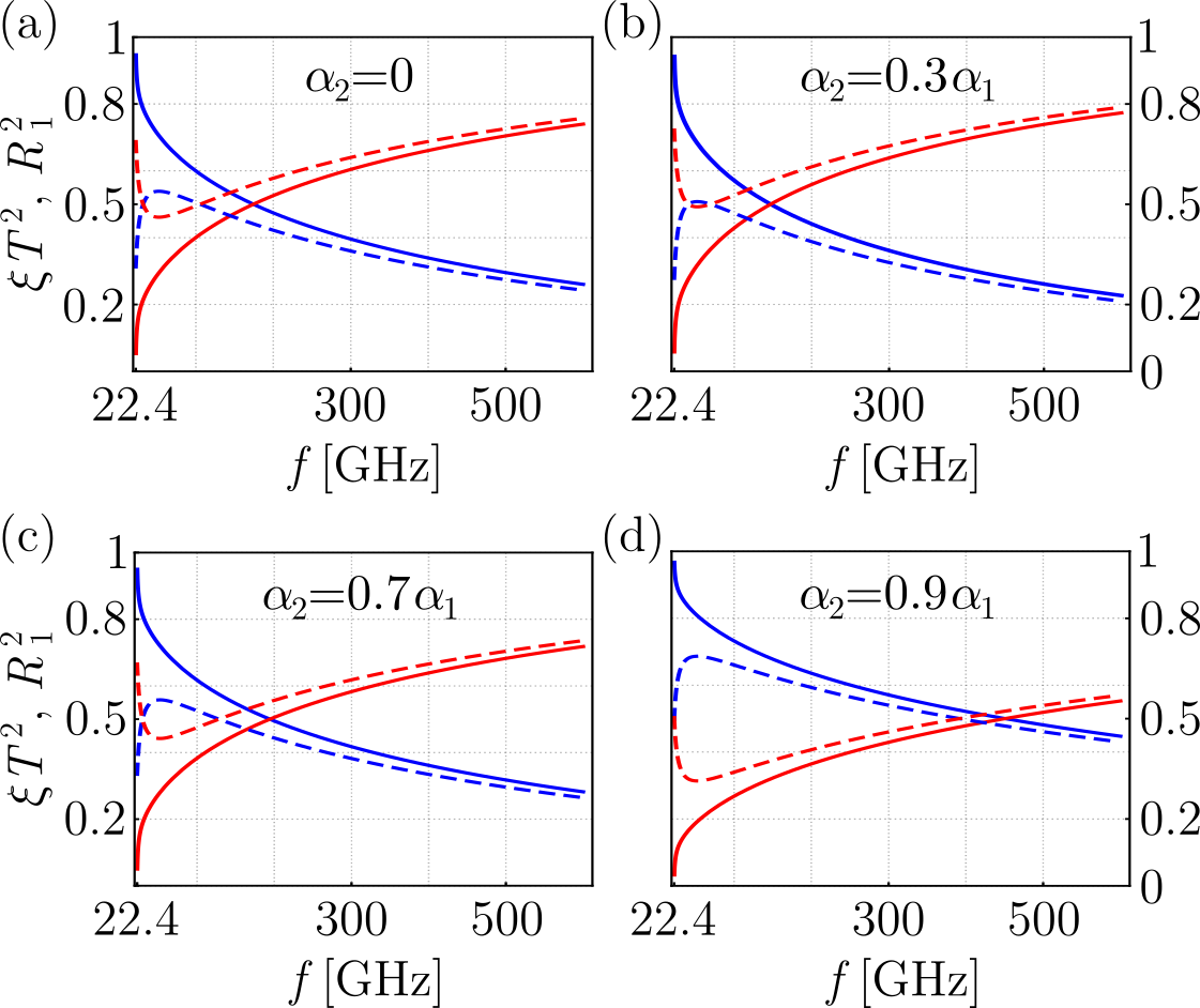
To control SW propagation via material parameters tuning, it is convenient to consider the dependence of the physical transmittance on frequency. We consider the vicinity of noncompensated case, i.e. when 999Despite the fact that the magnitudes of the magnetization in FM and sublattice magnetization in the AFM have to be approximately equal, i.e. , we have tested the limits of our model applicability for various values of within the range , thus confirming that it only leads to quantitative variations.. Since for , the SWs in AFM cannot propagate, we only consider the range . The case is shown in Fig. 3(a), where on the plus AFM branch the physical transmittance increases monotonously, while on the minus AFM branch it decreases up to a certain frequency and then increases again. Moreover, at high frequencies the physical transmittances for both AFM branches converge. At very higher frequencies ( 6 THz), reaches maximum value of 1 and then decreases to zero (and respectively the reflectance reaches minimum value of 0 and then increases at to 1) 101010See Sec. V of the Supplemental Material [59]. Therefore, the full SW reflection or full transmission can be achieved at certain . The cases for different ratios are shown in Fig. 3(b)-(d). When , see Fig. 3(b), for the minus AFM branch, the physical transmittance does not drop below . Note that at higher frequencies in this range, the physical transmittance is always larger than the reflectance at any . Meanwhile, to obtain in a lower-frequency range, it is enough to use the minus AFM branch, as shown in Fig. 3. The phase shifts between the incident and reflected SWs and are always equal to , whereas the phase shift between the incident and transmitted SW .
Discussion. Most of the aspects of our SW propagation theory are applicable for any values of the DSNA , except for the boundary conditions (2), which are valid only in the vicinity of , i.e., for nearly noncompensated AFM/FM interface. Therefore, if one finds the way to generalize these conditions to any , the entire theory is immediately extended to any DSNA, thus covering the full range of AFM/FM interfaces: compensated, noncompensated, and anywhere in between. Then our model would also describe AFM/FM interfaces with not only flat profiles, but complex interfaces that take into account surface roughness, diagonal-like interfaces, and even curvilinear interfaces with variable DSNA. Furthermore, an analogous technique may be used to treat the SW propagation through AFM interfaces with other magnetic media.
Conclusions. We have demonstrated that introducing a new physical characteristic of a finite-thickness interface, the DSNA , makes an essential step towards describing a SW propagation through AFM/FM boundary. We have shown that in noncompensated case, by varying the exchange interaction parameter between AFM sublattices, , fine control of the SW transmittance through the AFM/FM interface can be achieved in the entire range from full reflection to full transmission depending on the SW frequency. This approach may open doors for tailoring interfaces with given AFM exchange constants for future magnonic nanodevices.
Acknowledgments. The authors are grateful to Prof. Yu. Gorobets for very fruitful discussions, who passed away during the preparation of this paper. O.B. and O.G. acknowledge him as a mentor, his guidance and support continue to live on through everyone who knew him. O.B. acknowledges the support of this work by the Academy of Finland (Grants No. 320086 and No. 346035). O.A.T. acknowledges the support by the Australian Research Council (Grant No. DP200101027), the Cooperative Research Project Program at the Research Institute of Electrical Communication, Tohoku University (Japan), and NCMAS grant.
References
- MacDonald and Tsoi [2011] A. H. MacDonald and M. Tsoi, Antiferromagnetic metal spintronics, Philos. Trans. R. Soc. A 369, 3098 (2011).
- Chumak et al. [2015] A. Chumak, V. Vasyuchka, A. Serga, and B. Hillebrands, Magnon spintronics, Nat. Phys. 11, 453 (2015).
- Baltz et al. [2018] V. Baltz, A. Manchon, M. Tsoi, T. Moriyama, T. Ono, and Y. Tserkovnyak, Antiferromagnetic spintronics, Rev. Mod. Phys. 90, 015005 (2018).
- Ni et al. [2021] Z. Ni, A. V. Haglund, H. Wang, B. Xu, C. Bernhard, D. G. Mandrus, X. Qian, E. J. Mele, C. L. Kane, and L. Wu, Imaging the Néel vector switching in the monolayer antiferromagnet MnPSe3 with strain-controlled ising order, Nat. Nanotechnol. 16, 782 (2021).
- Mohseni et al. [2021] M. Mohseni, Q. Wang, B. Heinz, M. Kewenig, M. Schneider, F. Kohl, B. Lägel, C. Dubs, A. V. Chumak, and P. Pirro, Controlling the nonlinear relaxation of quantized propagating magnons in nanodevices, Phys. Rev. Lett. 126, 097202 (2021).
- Yu et al. [2016] H. Yu, O. d’ Allivy Kelly, V. Cros, R. Bernard, P. Bortolotti, A. Anane, F. Brandl, F. Heimbach, and D. Grundler, Approaching soft X-ray wavelengths in nanomagnet-based microwave technology, Nat. Commun. 7, 11255 (2016).
- Hämäläinen et al. [2018] S. J. Hämäläinen, M. Madami, H. Qin, G. Gubbiotti, and S. van Dijken, Control of spin-wave transmission by a programmable domain wall, Nat. Commun. 9, 4853 (2018).
- Liu et al. [2018] C. Liu, J. Chen, T. Liu, F. Heimbach, H. Yu, Y. Xiao, J. Hu, M. Liu, H. Chang, T. Stueckler, S. Tu, Y. Zhang, Y. Zhang, P. Gao, Z. Liao, D. Yu, K. Xia, N. Lei, W. Zhao, and M. Wu, Long-distance propagation of short-wavelength spin waves, Nat. Commun. 9, 738 (2018).
- Kim et al. [2020] C. Kim, S. Lee, H.-G. Kim, J.-H. Park, K.-W. Moon, J. Y. Park, J. M. Yuk, K.-J. Lee, B.-G. Park, S. K. Kim, K.-J. Kim, and C. Hwang, Distinct handedness of spin wave across the compensation temperatures of ferrimagnets, Nat. Mater. 19, 980 (2020).
- Göbel et al. [2021] B. Göbel, I. Mertig, and O. A. Tretiakov, Beyond skyrmions: Review and perspectives of alternative magnetic quasiparticles, Phys. Rep. 895, 1 (2021).
- Mashkovich et al. [2019] E. A. Mashkovich, K. A. Grishunin, R. V. Mikhaylovskiy, A. K. Zvezdin, R. V. Pisarev, M. B. Strugatsky, P. C. M. Christianen, T. Rasing, and A. V. Kimel, Terahertz optomagnetism: Nonlinear THz excitation of GHz spin waves in antiferromagnetic , Phys. Rev. Lett. 123, 157202 (2019).
- Dabrowski et al. [2020] M. Dabrowski, T. Nakano, D. M. Burn, A. Frisk, D. G. Newman, C. Klewe, Q. Li, M. Yang, P. Shafer, E. Arenholz, T. Hesjedal, G. van der Laan, Z. Q. Qiu, and R. J. Hicken, Coherent transfer of spin angular momentum by evanescent spin waves within antiferromagnetic NiO, Phys. Rev. Lett. 124, 217201 (2020).
- Cenker et al. [2021] J. Cenker, B. Huang, N. Suri, P. Thijssen, A. Miller, T. Song, T. Taniguchi, K. Watanabe, M. A. McGuire, D. Xiao, and X. Xu, Direct observation of two-dimensional magnons in atomically thin CrI3, Nat. Phys. 17, 20 (2021).
- Rezende [2020] S. M. Rezende, Fundamentals of Magnonics, Vol. 969 (Springer, 2020).
- Němec et al. [2018] P. Němec, M. Fiebig, T. Kampfrath, and A. V. Kimel, Antiferromagnetic opto-spintronics, Nat. Phys. 14, 229 (2018).
- Zhang et al. [2020] X. Zhang, L. Li, D. Weber, J. Goldberger, K. F. Mak, and J. Shan, Gate-tunable spin waves in antiferromagnetic atomic bilayers, Nat. Mater. 19, 838 (2020).
- Maendl et al. [2017] S. Maendl, I. Stasinopoulos, and D. Grundler, Spin waves with large decay length and few 100 nm wavelengths in thin yttrium iron garnet grown at the wafer scale, Appl. Phys. Lett. 111, 012403 (2017).
- Gubbiotti et al. [2010] G. Gubbiotti, S. Tacchi, M. Madami, G. Carlotti, A. O. Adeyeye, and M. Kostylev, Brillouin light scattering studies of planar metallic magnonic crystals, J. Phys. D: Appl. Phys. 43, 264003 (2010).
- Ulrichs and Razdolski [2018] H. Ulrichs and I. Razdolski, Micromagnetic view on ultrafast magnon generation by femtosecond spin current pulses, Phys. Rev. B 98, 054429 (2018).
- Yin et al. [2019] G. Yin, J. X. Yu, Y. Liu, R. K. Lake, J. Zang, and K. L. Wang, Planar Hall Effect in Antiferromagnetic MnTe Thin Films, Phys. Rev. Lett. 122, 106602 (2019).
- Železný et al. [2014] J. Železný, H. Gao, K. Výborný, J. Zemen, J. Mašek, A. Manchon, J. Wunderlich, J. Sinova, and T. Jungwirth, Relativistic Néel-order fields induced by electrical current in antiferromagnets, Phys. Rev. Lett. 113, 157201 (2014).
- Cheng et al. [2014] R. Cheng, J. Xiao, Q. Niu, and A. Brataas, Spin pumping and spin-transfer torques in antiferromagnets, Phys. Rev. Lett. 113, 057601 (2014).
- Shick et al. [2010] A. B. Shick, S. Khmelevskyi, O. N. Mryasov, J. Wunderlich, and T. Jungwirth, Spin-orbit coupling induced anisotropy effects in bimetallic antiferromagnets: A route towards antiferromagnetic spintronics, Phys. Rev. B 81, 212409 (2010).
- Wadley et al. [2017] P. Wadley, K. W. Edmonds, M. R. Shahedkhah, R. P. Campion, B. L. Gallagher, J. Železný, J. Kuneš, V. Novák, T. Jungwirth, V. Saidl, P. Němec, F. Maccherozzi, and S. S. Dhesi, Control of antiferromagnetic spin axis orientation in bilayer Fe/CuMnAs films, Sci. Rep. 7, 11147 (2017).
- Shen et al. [2020] L. Shen, J. Xia, X. Zhang, M. Ezawa, O. A. Tretiakov, X. Liu, G. Zhao, and Y. Zhou, Current-induced dynamics and chaos of antiferromagnetic bimerons, Phys. Rev. Lett. 124, 037202 (2020).
- Wang et al. [2019] H. Wang, C. Lu, J. Chen, Y. Liu, S. L. Yuan, S. W. Cheong, S. Dong, and J. M. Liu, Giant anisotropic magnetoresistance and nonvolatile memory in canted antiferromagnet Sr2IrO4, Nat. Commun. 10, 2280 (2019).
- Scott [1985] J. C. Scott, Ferromagnetic resonance studies in the bilayer system Ni0.80Fe0.20/Mn0.50Fe0.50: Exchange anisotropy, J. Appl. Phys. 57, 3681 (1985).
- DuttaGupta et al. [2020] S. DuttaGupta, A. Kurenkov, O. A. Tretiakov, G. Krishnaswamy, G. Sala, V. Krizakova, F. Maccherozzi, S. S. Dhesi, P. Gambardella, S. Fukami, and H. Ohno, Spin-orbit torque switching of an antiferromagnetic metallic heterostructure, Nat. Commun. 11, 5715 (2020).
- Mikhailov et al. [2017] G. M. Mikhailov, A. V. Chernykh, and L. A. Fomin, Application of magnetic force microscopy for investigation of epitaxial ferro- and antiferromagnetic structures, Materials 10, 1156 (2017).
- Gruyters and Schmitz [2008] M. Gruyters and D. Schmitz, Microscopic nature of ferro- and antiferromagnetic interface coupling of uncompensated magnetic moments in exchange bias systems, Phys. Rev. Lett. 100, 077205 (2008).
- Puliafito et al. [2019] V. Puliafito, R. Khymyn, M. Carpentieri, B. Azzerboni, V. Tiberkevich, A. Slavin, and G. Finocchio, Micromagnetic modeling of terahertz oscillations in an antiferromagnetic material driven by the spin Hall effect, Phys. Rev. B 99, 024405 (2019).
- Kampfrath et al. [2011] T. Kampfrath, A. Sell, G. Klatt, A. Pashkin, S. Mährlein, T. Dekorsy, M. Wolf, M. Fiebig, A. Leitenstorfer, and R. Huber, Coherent terahertz control of antiferromagnetic spin waves, Nat. Photonics 5, 31 (2011).
- Tveten et al. [2016] E. G. Tveten, T. Müller, J. Linder, and A. Brataas, Intrinsic magnetization of antiferromagnetic textures, Phys. Rev. B 93, 104408 (2016).
- Lee et al. [2019] D. K. Lee, B. G. Park, and K. J. Lee, Antiferromagnetic Oscillators Driven by Spin Currents with Arbitrary Spin Polarization Directions, Phys. Rev. Appl. 11, 054048 (2019).
- Shen et al. [2019] L. Shen, J. Xia, G. Zhao, X. Zhang, M. Ezawa, O. A. Tretiakov, X. Liu, and Y. Zhou, Spin torque nano-oscillators based on antiferromagnetic skyrmions, Appl. Phys. Lett. 114, 042402 (2019).
- Chen et al. [2018] X. Z. Chen, R. Zarzuela, J. Zhang, C. Song, X. F. Zhou, G. Y. Shi, F. Li, H. A. Zhou, W. J. Jiang, F. Pan, and Y. Tserkovnyak, Antidamping-Torque-Induced Switching in Biaxial Antiferromagnetic Insulators, Phys. Rev. Lett. 120, 207204 (2018).
- Shiino et al. [2016] T. Shiino, S. H. Oh, P. M. Haney, S. W. Lee, G. Go, B. G. Park, and K. J. Lee, Antiferromagnetic Domain Wall Motion Driven by Spin-Orbit Torques, Phys. Rev. Lett. 117, 087203 (2016).
- Baldrati et al. [2019] L. Baldrati, O. Gomonay, A. Ross, M. Filianina, R. Lebrun, R. Ramos, C. Leveille, F. Fuhrmann, T. R. Forrest, F. MacCherozzi, S. Valencia, F. Kronast, E. Saitoh, J. Sinova, and M. Klaüi, Mechanism of Néel Order Switching in Antiferromagnetic Thin Films Revealed by Magnetotransport and Direct Imaging, Phys. Rev. Lett. 123, 177201 (2019).
- Belashchenko et al. [2016] K. D. Belashchenko, O. Tchernyshyov, A. A. Kovalev, and O. A. Tretiakov, Magnetoelectric domain wall dynamics and its implications for magnetoelectric memory, Applied Physics Letters 108, 132403 (2016).
- Moriyama et al. [2018] T. Moriyama, K. Oda, T. Ohkochi, M. Kimata, and T. Ono, Spin torque control of antiferromagnetic moments in NiO, Sci. Rep. 8, 14167 (2018).
- Khymyn et al. [2016] R. Khymyn, I. Lisenkov, V. S. Tiberkevich, A. N. Slavin, and B. A. Ivanov, Transformation of spin current by antiferromagnetic insulators, Phys. Rev. B 93, 224421 (2016).
- Buchner et al. [2019] M. Buchner, B. Henne, V. Ney, and A. Ney, Transition from a hysteresis-like to an exchange-bias-like response of an uncompensated antiferromagnet, Phys. Rev. B 99, 064409 (2019).
- Tretiakov et al. [2017] O. A. Tretiakov, M. Morini, S. Vasylkevych, and V. Slastikov, Engineering curvature-induced anisotropy in thin ferromagnetic films, Phys. Rev. Lett. 119, 077203 (2017).
- Xue et al. [2015] X. Xue, Z. Zhou, B. Peng, M. Zhu, Y. Zhang, W. Ren, T. Ren, X. Yang, T. Nan, N. X. Sun, and M. Liu, Electric field induced reversible 180∘ magnetization switching through tuning of interfacial exchange bias along magnetic easy-axis in multiferroic laminates, Sci. Rep. 5, 16480 (2015).
- Li et al. [2013] B. Li, W. Liu, X. G. Zhao, S. Guo, W. J. Gong, J. N. Feng, T. Yu, and Z. D. Zhang, Modification of exchange bias by cooling field without changing the ferromagnetic magnetization, J. Magn. Magn. Mater. 332, 71 (2013).
- Ślȩzak et al. [2019] M. Ślȩzak, T. Ślȩzak, P. Dróżdż, B. Matlak, K. Matlak, A. Kozioł-Rachwał, M. Zaja̧c, and J. Korecki, How a ferromagnet drives an antiferromagnet in exchange biased CoO/Fe(110) bilayers, Sci. Rep. 9, 889 (2019).
- Demeter et al. [2012] J. Demeter, E. Menéndez, A. Schrauwen, A. Teichert, R. Steitz, S. Vandezande, A. R. Wildes, W. Vandervorst, K. Temst, and A. Vantomme, Exchange bias induced by O ion implantation in ferromagnetic thin films, J. Phys. D: Appl. Phys. 45, 405004 (2012).
- Kruglyak et al. [2014] V. V. Kruglyak, O. Y. Gorobets, Y. I. Gorobets, and A. N. Kuchko, Magnetization boundary conditions at a ferromagnetic interface of finite thickness, J. Phys. Condens. Matter 26, 406001 (2014).
- Cochran and Heinrich [1992] J. F. Cochran and B. Heinrich, Boundary conditions for exchange-coupled magnetic slabs, Phys. Rev. B 45, 13096 (1992).
- Kłos et al. [2018] J. W. Kłos, Y. S. Dadoenkova, J. Rychły, N. N. Dadoenkova, I. L. Lyubchanskii, and J. Barnaś, Hartman effect for spin waves in exchange regime, Sci. Rep. 8, 17944 (2018).
- Note [1] The dissipation generally decreases the amplitudes of SWs, but does not influence their behavior qualitatively. Therefore, in the following we can use the LL equation approximation, where the dissipation is neglected.
- Bar’yakhtar et al. [1985] V. G. Bar’yakhtar, B. A. Ivanov, and M. V. Chetkin, Dynamics of domain walls in weak ferromagnets, Sov. Phys. Usp. 28, 563 (1985).
- Bar’yakhtar et al. [1980] V. Bar’yakhtar, B. Ivanov, and A. Sukstanskiǐ, Nonlinear waves and the dynamics of domain walls in weak ferromagnets, Sov. Phys. JETP 51, 757 (1980).
- Tveten et al. [2013] E. G. Tveten, A. Qaiumzadeh, O. A. Tretiakov, and A. Brataas, Staggered dynamics in antiferromagnets by collective coordinates, Phys. Rev. Lett. 110, 127208 (2013).
- J. Barnas [1991] J. Barnas, On the Hoffmann boundary conditions at the interface between two ferromagnets, J. Magn. Magn. Mater. 102, 319 (1991).
- Busel et al. [2018] O. Busel, O. Gorobets, and Y. Gorobets, Boundary conditions at the interface of finite thickness between ferromagnetic and antiferromagnetic materials, J. Magn. Magn. Mater. 462, 226 (2018).
- Busel et al. [2019] O. Busel, O. Gorobets, and Y. Gorobets, Propagation of Spin Waves Through an Interface Between Ferromagnetic and Antiferromagnetic Materials, J. Supercond. Nov. Magn. 32, 3097 (2019).
- Note [2] See Sec. I of the Supplemental Material [59].
- [59] See supplemental material at [url will be inserted by publisher] for additional information.
- Note [3] See Sec. II of the Supplemental Material [59].
- Note [4] We consider the interface as a composite material that includes three magnetizations - two from AFM sublattices and one from FM, as shown in Fig. (1). However, according to [48] for finding the boundary conditions in the form of Eqs. (2), the only case when magnetization of one of AFM sublattices is parallel and comparable in magnitude to the FM magnetization is appropriate, i.e., noncompensated AFM boundary case .
- Akhiezer et al. [1968] A. I. Akhiezer, V. G. Bar’yakhtar, and S. V. Peletminskii, Spin Waves (North-Holland, Amsterdam, 1968).
- Note [5] In realistic systems, the energy is lost at the boundary, however, generally this loss would not effect qualitatively the results of the proposed model if taken into account.
- Note [6] For the derivation of see Sec. IV of the Supplemental Material [59].
- Note [7] See Sec. IV of the Supplemental Material [59].
- Tveten et al. [2014] E. G. Tveten, A. Qaiumzadeh, and A. Brataas, Antiferromagnetic domain wall motion induced by spin waves, Phys. Rev. Lett. 112, 147204 (2014).
- Note [8] Note that at very high frequencies the LL equation stops being applicable and our description is not valid anymore.
- Note [9] Despite the fact that the magnitudes of the magnetization in FM and sublattice magnetization in the AFM have to be approximately equal, i.e. , we have tested the limits of our model applicability for various values of within the range , thus confirming that it only leads to quantitative variations.
- Note [10] See Sec. V of the Supplemental Material [59].