Ultraviolet Mie resonances in computationally discovered boron phosphide nanoparticles
Abstract
Controlling ultraviolet light at the nanoscale using optical Mie resonances holds great promise for a diverse set of applications, such as lithography, sterilization, and biospectroscopy. However, Mie resonances hosted by dielectric nanoantennas are difficult to realize at ultraviolet wavelengths due to the lack of both suitable materials and fabrication methods. Here, we systematically search for improved materials by computing the frequency dependent optical permittivity of 338 binary semiconductors and insulators from first principles, and evaluate their potential performance as high refractive index materials using Mie theory. Our analysis reveals several interesting candidate materials among which boron phosphide (BP) appears particularly promising. We then prepare BP nanoparticles and demonstrate that they support Mie resonances at visible and ultraviolet wavelengths using both far-field optical measurements and near-field electron energy-loss spectroscopy. We also present a laser reshaping method to realize spherical Mie-resonant BP nanoparticles. With a refractive index above 3 and low absorption losses, BP nanostructures advance Mie optics to the ultraviolet.
DTU] Department of Physics, Technical University of Denmark, Fysikvej, DK-2800 Kongens Lyngby, Denmark Kobe] Department of Electrical and Electronic Engineering, Kobe University, Rokkodai, Nada, Kobe 657-8501, Japan DTU] Department of Physics, Technical University of Denmark, Fysikvej, DK-2800 Kongens Lyngby, Denmark Kobe] Department of Electrical and Electronic Engineering, Kobe University, Rokkodai, Nada, Kobe 657-8501, Japan Kobe] Department of Electrical and Electronic Engineering, Kobe University, Rokkodai, Nada, Kobe 657-8501, Japan DTU] Department of Physics, Technical University of Denmark, Fysikvej, DK-2800 Kongens Lyngby, Denmark DTU] Department of Physics, Technical University of Denmark, Fysikvej, DK-2800 Kongens Lyngby, Denmark
Introduction
Achieving control over ultraviolet light with nanoscale materials is essential for improving surface-enhanced spectroscopies of biological molecules and enabling new ultraviolet optical components. Geometric Mie resonances supported by resonant nanoantennas made from materials that combine a high refractive index with low absorption losses offer efficient and tunable manipulation of the near- and far-field of optical waves1, 2. Mie resonances have been realized at visible and infrared wavelengths thanks to the mature lithographic processing of suitable materials3, such as silicon4, gallium phosphide5, and titanium dioxide6. It would be desirable to extend the operation of these materials to the ultraviolet, but their small direct band gap energies ( eV) lead to significant absorption losses in the ultraviolet. Recently, metasurfaces composed of an array of nanostructured materials with a wide band gap and moderate refractive index () have demonstrated wave front manipulation in the ultraviolet using waveguide modes7, 8, 9. For ultraviolet Mie optics, diamond has been theoretically suggested as a potential material 10, 11, but diamond comes with significant nanofabrication challenges12. Consequently, extending the rich optical properties of Mie resonances observed in the visible to the ultraviolet requires identification of new high-index materials as well as development of suitable fabrication methods to realize Mie-resonant nanoantennas.
Concurrent advances in first-principles methodology and computing power have recently made it possible to design and discover new materials via high-throughput computations13, 14, 15, 16, 17. The approach has been successfully applied in several domains, including photovoltaics, transparent conductors, and photocatalysis18, 19, 20. However, to the best of our knowledge, computational discovery of new high-index materials remains largely unexplored. Relevant previous work in this direction has been limited to the static response regime21, 22 reflecting the fact that the major materials databases so far has focused on ground state properties.
Here we use high-throughput linear response density functional theory (DFT) to screen an initial set of 2743 elementary and binary materials with the aim to identify isotropic high-index, low loss, and broad band optical materials. For the most promising materials, the computed frequency-dependent complex refractive indices are used as input for Mie scattering calculations to evaluate their optical performance. In addition to the already known high-index materials we identify several new compounds. In particular, boron phosphide (BP) offers a refractive index above 3 with very low absorption losses in a spectral range spanning from the infrared to the ultraviolet. We then prepare BP nanoparticles and show, by means of dark-field optical measurements and electron energy-loss spectroscopy, that they support size-dependent Mie resonances in the visible and ultraviolet. Finally, we demonstrate a laser reshaping method to realize spherical BP nanoparticles, which host multiple Mie resonances in quantitative agreement with full-field optical simulations.
Results
High-throughput screening
Our high-throughput screening procedure is illustrated in Fig. 1a. We build the workflow using the Python-based Atomic Simulation Recipes (ASR)23 framework and the MyQueue scheduling software24 (see detailed workflow in Supplementary Note 1 and Supplementary Fig. 1). Starting from 2743 thermodynamically stable elementary and binary materials from the Open Quantum Materials Database (OQMD)15 we extract the 1693 materials with up to 10 atoms in the unit cell and relax the atomic structure using DFT with the Perdew-Burke-Ernzerhof (PBE) exchange correlation functional25 and the D3 correction to account for the van der Waals forces26. We perform DFT ground state calculations for all of the materials to determine their electronic band gaps. After discarding the metals, we are left with 338 semiconductors for which we calculate the optical dielectric function, , within the random phase approximation (RPA) and extract the refractive index and extinction coefficient as and , respectively. All calculations are performed with the GPAW code27, 28.
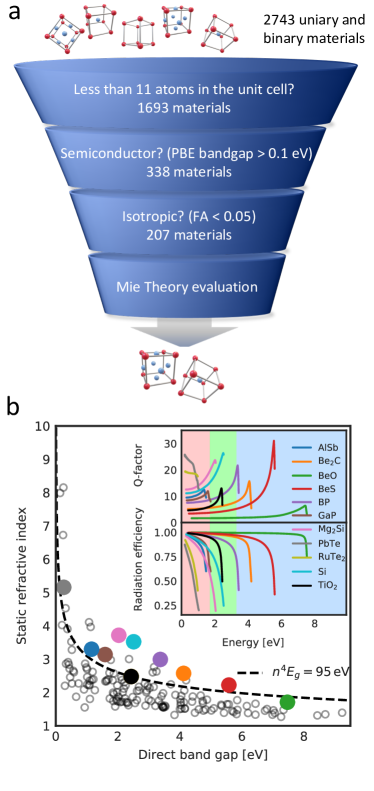
Next, we classify the materials according to the anisotropy of their refractive index tensor using a cut-off of 0.05 for the fractional anisotropy (see Supplementary Fig. 2). This leaves us with 207 isotropic material candidates, for which we show the static refractive index as a function of the direct band gap in Fig. 1b. The data points qualitatively follow the Moss formula29 (dashed line in Fig. 1b); however, there are significant deviations from the general trend, which we ascribe to variations in oscillator strength and density of the transitions across the direct gap. It is well known that (semi)local functionals like the PBE employed in the present work systematically underestimates band gaps30. This effect is, however, to some extent compensated by the fact that the RPA neglects the attractive electron-hole interactions and consequently underestimates the spectral weight near the band edge. As a result, refractive indices obtained with RPA@PBE are typically in good agreement with experiments in the static limit28 while deviations occur at higher frequencies near the band edge region (see Supplementary Note 2 and Supplementary Fig. 3-5). We shall return to this point later, but for now mention that for the materials that are identified as interesting based on this screening we will employ more accurate and computational expensive many-body perturbation methods.
We now turn to a more in-depth evaluation of the performance of the discovered materials. Specifically, we use Mie theory to calculate the scattering properties of a spherical nanoparticle made from the subset of isotropic materials. We focus on the lowest-order magnetic dipole (MD) resonance of the spheres and calculate energy-dependent quality factors, , and radiation efficiencies, (see Supplementary Note 1)3. This is achieved by continuously adjusting the size of the sphere to tune the energy of the MD resonance across the infrared, visible and ultraviolet regions. A high -factor is beneficial for boosting the local field enhancement of the nanoparticle, while a radiation efficiency close to unity points to low absorption losses. This analysis identifies all of the commonly used materials, such as Si, TiO2, and GaP. However, we also find a number of other highly promising materials, some of which are highlighted in the inset of Fig. 1b. In particular, we identify BP, which has a refractive index exceeding that of TiO2 and a radiation efficiency higher than both silicon and TiO2 across the entire visible part of the spectrum. For these reasons, we believe BP stands out as an overlooked material with highly desirable optical properties and we will focus on BP in the rest of the paper.
Optical response of BP

BP crystals were successfully synthesized as early as 195731, yet experimental measurements of its refractive index are limited to a couple of data points in the visible32, 33. Refractive index measurements of BP thin films have also been conducted but with varying results34, 35.
The RPA@PBE permittivities used for the initial screening are qualitatively accurate but suffer from underestimated band gaps and missing excitonic effects. To determine the refractive index of BP with quantitative accuracy, we solve the Bethe-Salpeter equation (BSE) to obtain the permittivity using single-particle transition energies obtained from a G0W0 band structure calculation. The band structure calculation reveals an indirect band gap of 2.1 eV and a direct band gap of 4.41 eV, which matches experimental measurements of the band gap energies for BP.36, 37 The square root dependence of the refractive index on the permittivity makes it crucial to converge both the real and imaginary parts of the latter. Unfortunately, the real part converges slowly with the number of bands making it impractical to obtain well converged results directly from the BSE. The problem can be alleviated by extending the imaginary part of the permittivity by an exponentially decaying tail whose weight is fixed by the f-sum rule (see Methods), and subsequently obtain the real part via the Kramers–Kronig relation. We benchmark this approach against experimental data for the refractive index of crystalline silicon and find excellent agreement (see Supplementary Note 3 and Supplementary Fig. 6).
With the f-sum rule fulfilling BSE-G0W0 method at hand, we are in a position to make a quantitative comparison of the refractive index of BP with some of the commonly used materials38, 39 in the visible as well as diamond40, which has been theoretically suggested for operation in the ultraviolet (Fig. 2a,b). We observe that the absorption edge of BP lies significantly higher than silicon, GaP, and TiO2, while it retains a refractive index comparable to that of GaP. This suggests that BP provides low-loss operation across the entire visible spectrum. While this is also the case for TiO2, its refractive index is significantly lower than that of BP. The higher refractive index of BP means that nanostructures can be made more compact41 and packed more densely for enhanced metasurface performance42. Importantly, we note that BP offers a high refractive index with a low extinction coefficient not only in the visible but also in the ultraviolet – a spectral region which is unreachable with the commonly-used materials. Diamond is transparent in the ultraviolet as well, but has a significantly lower refractive index. We illustrate the broadband performance of BP by performing extinction efficiency calculations using Mie theory for a BP sphere with varying radii, confirming that Mie resonances can be sustained across the visible and ultraviolet (Fig. 2c).
Far- and near-field characterization of BP nanoparticles
We now turn to an experimental demonstration of the potential of BP as a Mie-resonant nanostructure. BP has been synthesized in various forms such as crystals43, 44, films35, 45, 46, and nanoparticles47, 48, 49. However, BP nanoparticles in the size range suitable for sustaining Mie resonances have not been reported. We prepare BP nanoparticles in the size range of a few hundred nanometers by grounding BP powder (Kojundo Chemicals) in a mortar and then dispersing it in methanol. The BP solution is subsequently dropcasted on a glass substrate.
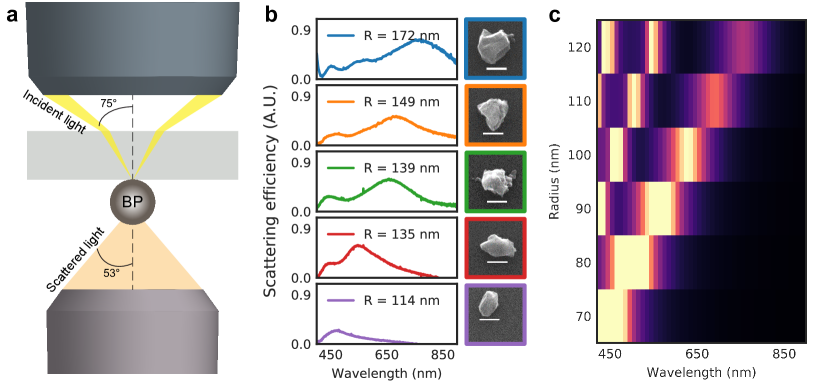
We measure the far-field scattering efficiency of individual nanoparticles by illuminating the nanoparticles through a high-numerical-aperture dark-field objective and collecting the transmitted scattered light (see Fig. 3a). A similar measurement setup has been used to detect Mie resonances in silicon nanoparticles.50 The scattering spectra recorded from a series of BP nanoparticles clearly show resonant peaks, which red shift with increasing particle size (Fig. 3b). Despite the irregular particle shapes, the scattering resonances are quite prominent and follow the trend observed in other Mie-resonant nanostructures, namely, that the smallest particle size support only the lowest-order Mie resonance while larger particle sizes also support higher-order Mie resonances51. We additionally confirm the crystallinity of the nanoparticles using micro-Raman spectroscopy from individual nanoparticles (see Supplementary Fig. 7). The particle radii are extracted from the scanning electron microscopy images under the assumption of a spherical shape and used as input for full-field simulations of the scattering efficiency of a BP nanosphere. The simulations account for the measurement setup as well as the glass substrate (see Methods). We find that the simulations accurately reproduce both the shift in resonance wavelengths with particle size as well as the number of resonant peaks (Fig. 3c). However, the particle sizes need to be adjusted to match the resonance wavelengths observed in the experiments. This suggests that the particle shape is better characterized as flakes with a thickness significantly smaller than the in-plane size. Nonetheless, the distinctive, multiple scattering peaks provide strong evidence for the interpretation that these are related to geometric Mie resonances.
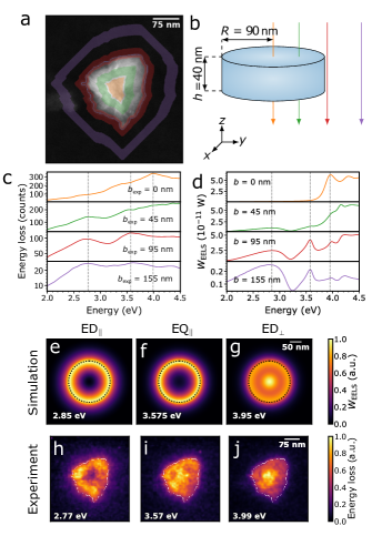
To gain more insight into the nature of these resonances and to access the ultraviolet spectral region, we also perform near-field characterization on similar BP nanoparticles using electron energy-loss spectroscopy (EELS). EELS is performed in a transmission electron microscope and has been employed to access near-field properties of both metallic52, 53 and dielectric nanostructures54, 55, 56 as well as optical devices57. The combined high spatial and spectral resolution of EELS provides unique nanoscale information on optical modes over a broad spectral range. For EELS measurements, the BP nanoparticles are deposited on a thin silicon oxide membrane. The EELS signal recorded from a triangular-shaped BP nanoparticle (Fig. 4a) at different beam positions is presented in Fig. 4c. The position of the beam is directly related to the excitation efficiency of the optical modes 58, and thus, by judicious positioning of the beam we can selectively excite different Mie modes. 54 When the beam is positioned in the center of nanoparticle, we observe a distinct resonance in the ultraviolet at 3.99 eV. As the beam is moved closer to the surface of the nanoparticle, two additional resonances are observed at the energies 3.57 eV and 2.77 eV. To identify the nature of these resonances, we simulate the EELS signal of a BP nanodisk with the same effective radius as the measured BP nanoparticle (Fig. 4b). The thickness of the nanodisk is varied to achieve correspondence to the measured EELS resonance energies. The simulated EELS spectra for a nanodisk thickness of nm at the same beam positions as in the experiments are shown in Fig. 4d. Here, we observe that the three lowest-energy EELS peaks have the same dependence on the impact parameter of the electron beam as seen experimentally. The simulated resonance energies of all three EELS peaks are also in quantitative agreement with the experiments, albeit the lowest-energy EELS peak is slightly shifted to higher energies in the simulations. The measured EELS peaks are broadened by the finite energy resolution of our EELS setup (see Methods). By performing a multipole decomposition of the induced field produced by the electron beam59, we identify the two lowest energy EELS peaks to be due to the Mie modes of the in-plane electric dipole ED∥ and in-plane electric quadrupole EQ∥. The highest energy EELS peak has contributions from both the in-plane magnetic dipole and and out-of-plane electric dipole ED⟂, where the latter dominates in the center of the particle (see Supplementary Fig. 8 for full decomposition). Simulated EELS intensity maps show that the electron beam couples efficiently to the in-plane modes, ED∥ and EQ∥ for beam positions near the surface of the particle, while the out-of-plane ED⟂ is excited also for beam positions in the center of the particle (Fig. 4e-g). The experimental EELS intensity maps of these three Mie modes are in good agreement with the simulations (Fig. 4h-j) as well as previous EELS measurements performed on Mie-resonant silicon nanoparticles54, 55. The near-field EELS measurements along with far-field dark-field optical measurements demonstrate that, despite their irregular shape, BP nanoparticles host a variety of multipolar size-dependent Mie resonances across the visible and ultraviolet, which are key attributes of low-loss high-index nanostructures.
Laser reshaping
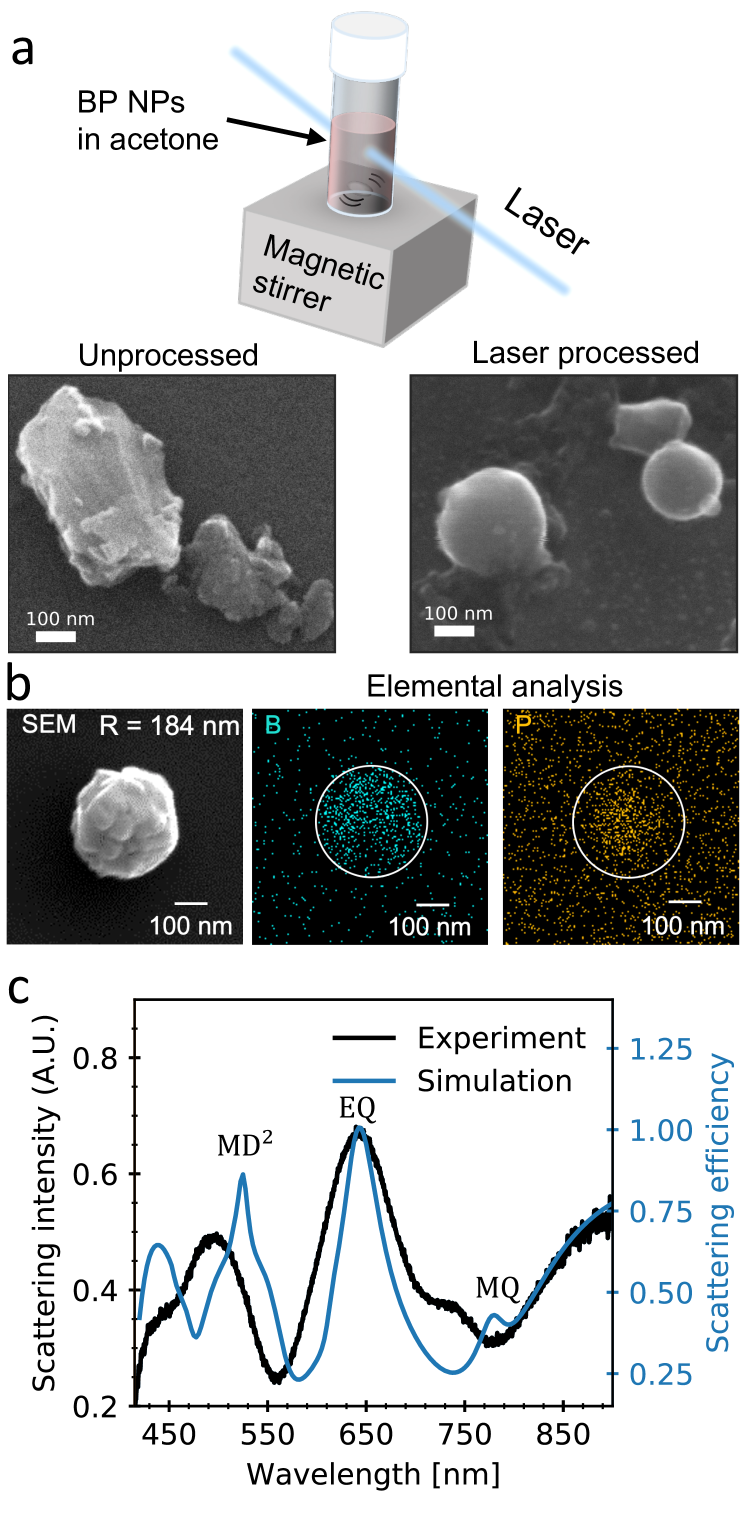
To alleviate the irregular shape of the as-prepared BP nanoparticles, we generate spherical BP nanoparticles by irradiating the unprocessed BP nanoparticles with a pulsed laser (see Fig. 5a and Methods). An example of a laser-processed BP nanoparticle is presented in Fig. 5b, confirming that the laser processing can be used for realizing spherical-shaped BP nanoparticles without affecting the nanoparticle composition. In addition, we perform micro-Raman spectroscopy on the same particle and find that the crystallinity from the unprocessed BP nanoparticles is retained after laser reshaping (see Supplementary Fig. 7). The dark-field scattering spectrum from the BP nanoparticle in Fig. 5b is recorded and we observe multiple scattering peaks (Fig. 5c). The relatively large particle radius ( nm) places the lowest-order Mie resonances at wavelengths longer than our measurement range, while the scattering peaks observed can be attributed to higher-order Mie resonances. The full-field simulation of a BP nanosphere with a slightly smaller radius nm, where we account for the substrate and the measurement setup, shows very good agreement with the measurement. We attribute the deviation in particle radius to shape imperfections and a slight variation between the calculated and experimental refractive index of BP. Multipole decomposition reveals that the scattering peaks are due to the excitation of the magnetic quadrupole MQ, the electric quadrupole EQ, and radial higher-order magnetic dipole MD2, thereby confirming the Mie-resonant nature of BP nanoparticles. We also performed EELS measurements on a smaller laser-reshaped BP nanoparticle, where we observe Mie resonances in the ultraviolet (see Supplementary Fig. 9).
Discussion
Using a DFT-based high-throughput screening method combined with optical Mie theory of 338 dielectrics, we identify BP as a promising high-refractive-index material for ultraviolet nanooptics. We develop a new, quantitatively accurate many-body perturbation theory based methodology for calculating refractive indices and use it to reveal that BP has a high refractive index () and low extinction coefficient () up to ultraviolet photon energies of 4 eV. We present an approach to fabricate BP nanoparticles as well as a laser reshaping method to generate spherical BP nanoparticles. Through dark-field optical spectroscopy and EELS measurements, we confirm the presence of Mie resonances in BP nanoparticles across the visible and ultraviolet. Our work advances nanoscale Mie optics to the ultraviolet and may find applications in metasurface-enhanced spectroscopy of biological molecules and, more generally, in realizing metasurface optical components operating in the ultraviolet.
Methods
Computational workflow
Structural relaxation:
All ground- and excited state calculations were performed with the GPAW electronic structure code27. We relaxed the atomic structure and the unit cell of the materials until the maximum force (stress) is below eV/Å (0.002eV/Å3). We use the PBE functional for exchange and correlation effects, a -point centered k-point grid with a density of Å-3, a 800 eV plane wave cutoff and a Fermi-Dirac smearing of 50 meV. Van der Waals interactions were taken into account by the D3 correction scheme26.
RPA calculations:
We calculate the optical permittivity, , within the Random Phase Approximation(RPA) using the dielectric function module in GPAW. From we calculate the refractive index and extinction coefficient as and respectively. To ensure convergence across all materials we employ a k-point grid with a high density of 20.0 Å-3 and include conduction bands up to 5 times the number of valence bands. The calculations were performed on a nonlinear frequency grid with an initial frequency spacing of 0.5 meV, a broadening of 50 meV and a local field cutoff of 50 eV.
Many-body perturbation theory calculations
G0W0 calculations:
The G0W0 calculations were performed on top of the ground state calculations. To ensure converged quasi-particle gaps we perform extrapolation of both the plane wave cut-off and the k-point resolution to infinity.
BSE calculations:
The BSE calculations were performed within the Tamm-Dancoff approximation on a k-point grid with a density of 20 Å-3. The calculation included all valence and conduction bands within 2.3 eV of the valence band maximum and conduction minimum, respectively. The calculation of the screened interaction included all occupied bands and unoccupied bands up to 5 times the number of occupied bands, and we accounted for local field effects up to a plane wave cut-off of 50 eV. The calculation was performed on a linear 10001 point frequency grid spanning 0 to 8 eV.
BSE f-sum rule correction
The optical polarizability has to obey the f-sum rule,
| (1) |
where is the electron density, is the elementary charge and is the electron mass. Since it is not obvious what to use for in our PAW calculations, we use a different strategy to fix the left hand side, namely we obtain it from an RPA calculation (which can be readily converged)
| (2) |
Eq. 2 can be enforced if we artificially extend the imaginary part of the BSE polarizability. Denoting the largest transition energy included in the BSE calculation as , we perform the following extension,
| (3) |
The constant is used to ensure continuity and the constant is fixed to give the correct spectral weight as fixed by Eq. 2. For benchmarks see Supplementary Information.
Optical simulations
The scattering efficiency and EELS simulations are both performed in COMSOL Multiphysics (ver. 5.6), which solves Maxwell’s equations using finite-element modelling. For the scattering efficiency simulations in Fig. 3c, a BP sphere is placed on a semi-infinite glass substrate () and excited by a plane wave incident from the substrate side at an oblique angle of . We use the f-sum corrected refractive index for BP shown in Fig. 2. We then perform a near-to-far field transformation to extract the scattered far-field60. The Poynting flux of the scattered far-field in the air region is integrated over a solid angle spanning an azimuthal angle of and a maximum polar angle of to retrieve the total scattered power collected by the collection objective (). The total scattered power is normalized to the incident power and the geometrical cross sectional area of the particle to determine the scattering efficiency. To account for the unpolarized incident light in the experiments, we perform this simulation procedure for both transverse-electric and transverse-magnetic polarization of the incident wave. Finally, the scattering efficiency from both polarization states is averaged. The scattering efficiency simulation in Fig. 5c follows the same steps with the only change being that the plane wave is incident from the air side at an oblique angle of .
For the EELS calculations, we simulate the electron beam as an edge current with an amplitude of 1 µA. The induced electromagnetic field is obtained by calculating the fields with and without the BP nanodisk in the simulation domain, and subsequently subtracting them. The energy loss is then calculated as the work rate done on the electron beam by the induced electromagnetic field 54.
Dark-field scattering measurements
A custom-built inverted optical microscope was used for dark-field scattering spectroscopy of single nanoparticles (Fig. 3a). For the measurements presented in Fig. 3, the sample is illuminated from the top by a halogen lamp through a dark field condenser and the scattered light was collected by an objective (50×, ). For the spectrum in Fig. 5c, the sample was illuminated from the bottom through a dark-field objective (50×, ) and the scattered light was collected by the same objective. To measure the spectra, scattered light was transferred to the entrance slit of a monochromator (SpectraPro-300i, Princeton Instruments) and detected by a liquid-N2 cooled CCD (Princeton Instruments). For Raman scattering measurements, the nanoparticles were excited by a 488 nm laser (Coherent Sapphire 488–50).
EELS measurements and analysis
The EELS measurements are performed in a monochromated and aberration-corrected FEI Titan operated in STEM mode at an acceleration voltage of 300 kV, providing a probe size of nm and an energy resolution of 0.08 eV (as measured by the full-width-at-half-maximum of the zero-loss peak). We perform Richardson–Lucy deconvolution to remove the zero-loss peak. An EELS spectrum recorded in vacuum is used as an input for the point-spread function. Due to a small asymmetry in the zero-loss peak, the deconvolution algorithm produced an artificial EELS peak in the energy range below 0.5 eV. However, the artificial peak did not overlap with any of the observed resonances and could be safely removed using a first-order logarithmic polynomial.
The depicted EELS spectra are obtained by integrating the deconvoluted EELS data around the experimental impact parameter . This parameter is directly related to the effective radius of the particle which is extracted as a radius of the circle with the effective area of the particle found from the STEM image. The effective area of the particle is the area which is enclosed by the boundaries obtained by Otsu’s thresholding of the STEM image. The integration parameter itself is calculated as a radius of the circle with the adjusted effective area of expanded/reduced initial boundaries. For the integration region centered at the nanoparticle, the experimental impact parameter changes from 0 to 0.3 and denotes the nanoparticle center. For the annulus-shaped regions, the experimental impact parameter denotes the mean of the inner and outer radii with a typical radius spread of 0.3 (for example, the green region in Figure 4(a) encloses the regions from 0.35 to 0.65). The depicted EELS spectra are smoothed with a Gaussian function ( eV).
The EELS maps are obtained by summing the deconvoluted EELS data in a spectral window of eV width centered at the resonance energies. The signal-to-noise ratio is improved by spatially binning the map, reducing the total number of pixels by a factor of 4. A Gaussian filter with pixels is applied to smooth the image.
Laser reshaping
Unprocessed BP nanoparticles in acetone are irradiated with the third harmonic of a Nd:YAG laser (355 nm wavelength, 5 nm pulse width, 20 Hz repetition rate) with a fluence of 50 mJ/cm2 per pulse for 10 min. {acknowledgement} S. R. and A. A. acknowledge support from the Independent Research Funding Denmark (7026-00117B). K. S. T. acknowledges support from the Center for Nanostructured Graphene (CNG) under the Danish National Research Foundation (project DNRF103) and from the European Research Council (ERC) under the European Union’s Horizon 2020 research and innovation program (Grant No. 773122, LIMA). K. S. T. is a Villum Investigator supported by VILLUM FONDEN (grant no. 37789). H. S. acknowledges support by JSPS KAKENHI Grant Numbers 21K14496.
Author contributions M. K. S. constructed the computational workflow, performed the screening, developed the f-sum approach, and prepared the figures. H. S. performed the structural and optical characterizations of nanoparticles. A. A. performed the EELS measurements, EELS analysis, EELS simulations, and prepared a figure. D. S. fabricated the nanoparticles and conducted laser shaping processes. M. F. contributed to analyses and interpretation of the data and supervised the fabrication and characterizations of nanoparticles. S. R. and K. S. T. conceived the idea and supervised the work. S. R. performed the optical simulations. All authors discussed the results and contributed to the preparation of the manuscript.
Conflict of interests The authors declare no competing financial interests.
Data and materials availability All data needed to evaluate the conclusions in the paper are present in the paper and/or the Supplementary Information. Additional data related to this paper may be requested from the corresponding author.
References
- Kuznetsov et al. 2016 Kuznetsov, A. I.; Miroshnichenko, A. E.; Brongersma, M. L.; Kivshar, Y. S.; Luk’yanchuk, B. Optically resonant dielectric nanostructures. Science 2016, 354, aag2472
- Kruk and Kivshar 2017 Kruk, S.; Kivshar, Y. Functional meta-optics and nanophotonics governed by Mie resonances. ACS Photonics 2017, 4, 2638–2649
- Baranov et al. 2017 Baranov, D. G.; Zuev, D. A.; Lepeshov, S. I.; Kotov, O. V.; Krasnok, A. E.; Evlyukhin, A. B.; Chichkov, B. N. All-dielectric nanophotonics: the quest for better materials and fabrication techniques. Optica 2017, 4, 814–825
- Staude and Schilling 2017 Staude, I.; Schilling, J. Metamaterial-inspired silicon nanophotonics. Nat. Photonics 2017, 11, 274–284
- Wilson et al. 2020 Wilson, D. J.; Schneider, K.; Hönl, S.; Anderson, M.; Baumgartner, Y.; Czornomaz, L.; Kippenberg, T. J.; Seidler, P. Integrated gallium phosphide nonlinear photonics. Nat. Photonics 2020, 14, 57–62
- Chen et al. 2018 Chen, W. T.; Zhu, A. Y.; Sanjeev, V.; Khorasaninejad, M.; Shi, Z.; Lee, E.; Capasso, F. A broadband achromatic metalens for focusing and imaging in the visible. Nat. Nanotechnol. 2018, 13, 220–226
- Huang et al. 2019 Huang, K.; Deng, J.; Leong, H. S.; Yap, S. L. K.; Yang, R. B.; Teng, J.; Liu, H. Ultraviolet Metasurfaces of 80% Efficiency with Antiferromagnetic Resonances for Optical Vectorial Anti-Counterfeiting. Laser Photon. Rev. 2019, 13, 1800289
- Zhang et al. 2020 Zhang, C.; Divitt, S.; Fan, Q.; Zhu, W.; Agrawal, A.; Lu, Y.; Xu, T.; Lezec, H. J. Low-loss metasurface optics down to the deep ultraviolet region. Light Sci. Appl. 2020, 9, 55
- Zhao et al. 2021 Zhao, D.; Lin, Z.; Zhu, W.; Lezec, H. J.; Xu, T.; Agrawal, A.; Zhang, C.; Huang, K. Recent advances in ultraviolet nanophotonics: from plasmonics and metamaterials to metasurfaces. Nanophotonics 2021, 10, 2283–2308
- Gutiérrez et al. 2018 Gutiérrez, Y.; Ortiz, D.; Saiz, J. M.; González, F.; Albella, P.; Moreno, F. The quest for low loss high refractive index dielectric materials for UV photonic applications. Appl. Sci. 2018, 8, 2065
- Hu et al. 2020 Hu, J.; Lawrence, M.; Dionne, J. A. High Quality Factor Dielectric Metasurfaces for Ultraviolet Circular Dichroism Spectroscopy. ACS Photonics 2020, 7, 36–42
- Aharonovich et al. 2011 Aharonovich, I.; Greentree, A. D.; Prawer, S. Diamond photonics. Nat. Photonics 2011, 5, 397–405
- Curtarolo et al. 2013 Curtarolo, S.; Hart, G. L.; Nardelli, M. B.; Mingo, N.; Sanvito, S.; Levy, O. The high-throughput highway to computational materials design. Nat. Mater. 2013, 12, 191–201
- Jain et al. 2013 Jain, A.; Ong, S. P.; Hautier, G.; Chen, W.; Richards, W. D.; Dacek, S.; Cholia, S.; Gunter, D.; Skinner, D.; Ceder, G., et al. Commentary: The Materials Project: A materials genome approach to accelerating materials innovation. APL Mater. 2013, 1, 011002
- Kirklin et al. 2015 Kirklin, S.; Saal, J. E.; Meredig, B.; Thompson, A.; Doak, J. W.; Aykol, M.; Rühl, S.; Wolverton, C. The Open Quantum Materials Database (OQMD): assessing the accuracy of DFT formation energies. NPJ Comput. Mater. 2015, 1, 15010
- Haastrup et al. 2018 Haastrup, S.; Strange, M.; Pandey, M.; Deilmann, T.; Schmidt, P. S.; Hinsche, N. F.; Gjerding, M. N.; Torelli, D.; Larsen, P. M.; Riis-Jensen, A. C., et al. The Computational 2D Materials Database: high-throughput modeling and discovery of atomically thin crystals. 2D Mater. 2018, 5, 042002
- Gjerding et al. 2021 Gjerding, M.; Taghizadeh, A.; Rasmussen, A.; Ali, S.; Bertoldo, F.; Deilmann, T.; Holguin, U.; Knøsgaard, N.; Kruse, M.; Manti, S., et al. Recent progress of the Computational 2D Materials Database (C2DB). 2D Materials 2021, 8, 044002
- Varley et al. 2017 Varley, J. B.; Miglio, A.; Ha, V.-A.; van Setten, M. J.; Rignanese, G.-M.; Hautier, G. High-throughput design of non-oxide p-type transparent conducting materials: Data mining, search strategy, and identification of boron phosphide. Chem. Mater. 2017, 29, 2568–2573
- Yu and Zunger 2012 Yu, L.; Zunger, A. Identification of potential photovoltaic absorbers based on first-principles spectroscopic screening of materials. Phys. Rev. Lett. 2012, 108, 068701
- Castelli et al. 2012 Castelli, I. E.; Olsen, T.; Datta, S.; Landis, D. D.; Dahl, S.; Thygesen, K. S.; Jacobsen, K. W. Computational screening of perovskite metal oxides for optimal solar light capture. Energy Environ. Sci. 2012, 5, 5814–5819
- Petousis et al. 2017 Petousis, I.; Mrdjenovich, D.; Ballouz, E.; Liu, M.; Winston, D.; Chen, W.; Graf, T.; Schladt, T. D.; Persson, K. A.; Prinz, F. B. High-throughput screening of inorganic compounds for the discovery of novel dielectric and optical materials. Sci. data 2017, 4, 160134
- Naccarato et al. 2019 Naccarato, F.; Ricci, F.; Suntivich, J.; Hautier, G.; Wirtz, L.; Rignanese, G.-M. Searching for materials with high refractive index and wide band gap: A first-principles high-throughput study. Phys. Rev. Mater. 2019, 3, 044602
- Gjerding et al. 2021 Gjerding, M.; Skovhus, T.; Rasmussen, A.; Bertoldo, F.; Larsen, A. H.; Mortensen, J. J.; Thygesen, K. S. Atomic Simulation Recipes–a Python framework and library for automated workflows. arXiv 2021, 2104.13431
- Mortensen et al. 2020 Mortensen, J. J.; Gjerding, M.; Thygesen, K. S. MyQueue: Task and workflow scheduling system. J. Open Source Softw. 2020, 5, 1844
- Perdew et al. 1996 Perdew, J. P.; Burke, K.; Ernzerhof, M. Generalized gradient approximation made simple. Phys. Rev. Lett. 1996, 77, 3865
- Grimme et al. 2010 Grimme, S.; Antony, J.; Ehrlich, S.; Krieg, H. A consistent and accurate ab initio parametrization of density functional dispersion correction (DFT-D) for the 94 elements H-Pu. J. Chem. Phys. 2010, 132, 154104
- Enkovaara et al. 2010 Enkovaara, J.; Rostgaard, C.; Mortensen, J. J.; Chen, J.; Dułak, M.; Ferrighi, L.; Gavnholt, J.; Glinsvad, C.; Haikola, V.; Hansen, H., et al. Electronic structure calculations with GPAW: a real-space implementation of the projector augmented-wave method. J. Phys. Condens. Matter 2010, 22, 253202
- Yan et al. 2011 Yan, J.; Mortensen, J. J.; Jacobsen, K. W.; Thygesen, K. S. Linear density response function in the projector augmented wave method: Applications to solids, surfaces, and interfaces. Phys. Rev. B 2011, 83, 245122
- Moss 1985 Moss, T. Relations between the refractive index and energy gap of semiconductors. physica status solidi (b) 1985, 131, 415–427
- Perdew 1985 Perdew, J. P. Density functional theory and the band gap problem. Int. J. Quantum Chem. 1985, 28, 497–523
- Popper and Ingles 1957 Popper, P.; Ingles, T. A. Boron Phosphide, a III–V Compound of Zinc-Blende Structure. Nature 1957, 179, 1075
- Takenaka et al. 1976 Takenaka, T.; Takigawa, M.; Shohno, K. Dielectric Constant and Refractive Index of Boron Monophosphide. Jpn. J. Appl. Phys. 1976, 15, 2021–2022
- Wettling and Windscheif 1984 Wettling, W.; Windscheif, J. Elastic constants and refractive index of boron phosphide. Solid State Commun. 1984, 50, 33–34
- Odawara et al. 2005 Odawara, M.; Udagawa, T.; Shimaoka, G. Organometallic chemical vapor deposition growth of heterostructure of wide band gap and transparent boron phosphide on silicon. Jpn. J. Appl. Phys. 2005, 44, 681–683
- Dalui et al. 2008 Dalui, S.; Hussain, S.; Varma, S.; Paramanik, D.; Pal, A. K. Boron phosphide films prepared by co-evaporation technique: Synthesis and characterization. Thin Solid Films 2008, 516, 4958–4965
- Archer et al. 1964 Archer, R. J.; Koyama, R. Y.; Loebner, E. E.; Lucas, R. C. Optical absorption, electroluminescence, and the band gap of BP. Phys. Rev. Lett. 1964, 12, 538–540
- Schroten et al. 1998 Schroten, E.; Goossens, A.; Schoonman, J. Photo- and electroreflectance of cubic boron phosphide. J. Appl. Phys. 1998, 83, 1660–1663
- Aspnes and Studna 1983 Aspnes, D. E.; Studna, A. Dielectric functions and optical parameters of si, ge, gap, gaas, gasb, inp, inas, and insb from 1.5 to 6.0 ev. Physical review B 1983, 27, 985
- Siefke et al. 2016 Siefke, T.; Kroker, S.; Pfeiffer, K.; Puffky, O.; Dietrich, K.; Franta, D.; Ohlídal, I.; Szeghalmi, A.; Kley, E.-B.; Tünnermann, A. Materials pushing the application limits of wire grid polarizers further into the deep ultraviolet spectral range. Advanced Optical Materials 2016, 4, 1780–1786
- Phillip and Taft 1964 Phillip, H.; Taft, E. Kramers-Kronig analysis of reflectance data for diamond. Physical Review 1964, 136, A1445
- Yang and Fan 2017 Yang, J.; Fan, J. A. Analysis of material selection on dielectric metasurface performance. Opt. Express 2017, 25, 23899–23909
- Lalanne and Chavel 2017 Lalanne, P.; Chavel, P. Metalenses at visible wavelengths: past, present, perspectives. Laser Photonics Rev. 2017, 11, 1600295
- Kumashiro 1990 Kumashiro, Y. Refractory semiconductor of boron phosphide. J. Mater. Res. 1990, 5, 2933–2947
- Woo et al. 2016 Woo, K.; Lee, K.; Kovnir, K. BP: Synthesis and properties of boron phosphide. Mater. Res. Express 2016, 3, 074003
- Kumashiro et al. 2011 Kumashiro, Y.; Nakamura, K.; Enomoto, T.; Tanaka, M. Preparation and thermoelectric properties of BP films on SOI and sapphire substrates. J. Mater. Sci. Mater. Electron. 2011, 22, 966–973
- Padavala et al. 2016 Padavala, B.; Frye, C. D.; Wang, X.; Ding, Z.; Chen, R.; Dudley, M.; Raghothamachar, B.; Lu, P.; Flanders, B. N.; Edgar, J. H. Epitaxy of Boron Phosphide on Aluminum Nitride(0001)/Sapphire Substrate. Cryst. Growth Des. 2016, 16, 981–987
- Sugimoto et al. 2015 Sugimoto, H.; Fujii, M.; Imakita, K. Size-controlled growth of cubic boron phosphide nanocrystals. RSC Adv. 2015, 5, 8427–8431
- Feng et al. 2019 Feng, M.; Zhang, J.; Zhou, H.; Jiang, P.; Zhang, D.; Wang, L.; Chen, S. Facile preparation of boron phosphide particles with high purity and high structural stability. Mater. Res. Express 2019, 6
- Sugimoto et al. 2019 Sugimoto, H.; Somogyi, B.; Nakamura, T.; Zhou, H.; Ichihashi, Y.; Nishiyama, S.; Gali, A.; Fujii, M. Size-dependent photocatalytic activity of cubic boron phosphide nanocrystals in the quantum confinement regime. J. Phys. Chem. C 2019, 123, 23226–23235
- Sugimoto and Fujii 2017 Sugimoto, H.; Fujii, M. Colloidal Dispersion of Subquarter Micrometer Silicon Spheres for Low-Loss Antenna in Visible Regime. Adv. Opt. Mater. 2017, 5, 1700332
- Sugimoto et al. 2020 Sugimoto, H.; Okazaki, T.; Fujii, M. Mie Resonator Color Inks of Monodispersed and Perfectly Spherical Crystalline Silicon Nanoparticles. Adv. Opt. Mater. 2020, 8, 2000033
- García de Abajo 2010 García de Abajo, F. J. Optical excitations in electron microscopy. Rev. Mod. Phys. 2010, 82, 209–275
- Colliex et al. 2016 Colliex, C.; Kociak, M.; Stéphan, O. Electron Energy Loss Spectroscopy imaging of surface plasmons at the nanometer scale. Ultramicroscopy 2016, 162, A1–A24
- Assadillayev et al. 2021 Assadillayev, A.; Hinamoto, T.; Fujii, M.; Sugimoto, H.; Brongersma, M. L.; Raza, S. Plasmon Launching and Scattering by Silicon Nanoparticles. ACS Photonics 2021, 8, 1582–1591
- Assadillayev et al. 2021 Assadillayev, A.; Hinamoto, T.; Fujii, M.; Sugimoto, H.; Raza, S. Thermal near-field tuning of silicon Mie nanoparticles. Nanophotonics 2021, 10, 4161–4169
- Alexander et al. 2021 Alexander, D. T.; Flauraud, V.; Demming-Janssen, F. Near-Field Mapping of Photonic Eigenmodes in Patterned Silicon Nanocavities by Electron Energy-Loss Spectroscopy. ACS Nano 2021, 15, 16501–16514
- Song et al. 2021 Song, J. H.; Raza, S.; van de Groep, J.; Kang, J. H.; Li, Q.; Kik, P. G.; Brongersma, M. L. Nanoelectromechanical modulation of a strongly-coupled plasmonic dimer. Nat. Commun. 2021, 12, 48
- Raza et al. 2016 Raza, S.; Esfandyarpour, M.; Koh, A. L.; Mortensen, N. A.; Brongersma, M. L.; Bozhevolnyi, S. I. Electron energy-loss spectroscopy of branched gap plasmon resonators. Nat. Commun. 2016, 7, 13790
- Alaee et al. 2018 Alaee, R.; Rockstuhl, C.; Fernandez-Corbaton, I. An electromagnetic multipole expansion beyond the long-wavelength approximation. Opt. Commun. 2018, 407, 17–21
- Yang et al. 2016 Yang, J.; Hugonin, J. P.; Lalanne, P. Near-to-Far Field Transformations for Radiative and Guided Waves. ACS Photonics 2016, 3, 395–402