Tracking and Vertex detectors at FCC-ee
Abstract
The combined vertexing and tracking performance of the innermost part of the FCC-ee experiments must deliver outstanding precision for measurement of the track momentum together with an impact parameter resolution exceeding by at least a factor five that typically achieved at LHC experiments. Furthermore, precision measurements require stability and fiducial accuracy at a level which is unprecedented in collider experiments. For the innermost vertex layers these goals translate into a target hit resolution of approximately 3 m together with a material budget of around 0.2% of a radiation length per layer. Typically this performance might be provided by silicon-based tracking, together with a careful choice of a low-mass cooling technology, and a stable, low mass mechanical structure capable of providing measurements with a low enough systematic error to match the tremendous statistics expected, particularly for the run around the Z resonance. At FCC-ee, the magnetic field will be limited to approximately 2 T, in order to contain the vertical emittance at the Z pole, and a tracking volume up to relative large radius is needed. The technological solution could be silicon or gaseous based tracking, in both cases with the focus on optimising the material budget, and particle identification capability would be an advantage. Depending on the global design, an additional silicon tracking layer could be added at the outer radius of the tracker to provide a final precise point contributing to the momentum or possibly time of flight measurement. Current developments in monolithic and hybrid silicon technology, as well as advanced gaseous tracking developments provide an encouraging road map towards the FCC-ee detector. The current state of the art and potential extensions will be discussed and a generic call for technology which could have a significant impact on the performance of an FCC-ee tracking and vertexing detector is outlined.
pacs:
PACS-keydiscribing text of that key and PACS-keydiscribing text of that key1 Introduction: tracking requirements for FCC-ee
The tracking volume which makes up the innermost part of any FCC-ee detector must be capable of delivering outstanding performance across the full acceptance, down to approximately 120 mrad, and full momentum range, typically with full efficiencies down to 300 MeV/c and 98% or better for muons down to 100 MeV/c transverse momentum. An overview of proposed detector layout and performance requirements can be found in the FCC-ee Conceptual Design Report (CDR) Abada:2019lih and in this issue Blondel:2021ema . A driving factor in the design is that the magnetic field will be limited to approximately 2 T, in order to contain the vertical emittance at the Z pole, and a tracking volume up to relatively large radius will therefore be needed. It must be engineered in a way which results in minimum material in front of the external detectors and a stable structure which is capable of providing measurements with a low enough systematic error to match the tremendous statistics expected, particularly for the Z pole running.
The role of the tracking system will be decisive for the FCC-ee physics goals. Examples of physics channels which place particular demands on the vertexing and tracking are listed here:
-
•
The clean environment in which the Higgs will be produced at FCC-ee, with 1M ZH events expected at 240 GeV blas , gives a unique opportunity to explore all decay modes, hence the importance of excellent b, c and tagging, placing high demands on the quality of the impact parameter resolution and secondary vertex resolution.
-
•
Another unique feature of the clean Higgs production via “Higgsstrahlung” is the possibility of reconstructing the Higgs recoil mass against the Z boson blas . In order to fully benefit from this, an excellent momentum resolution is required from the main tracker.
-
•
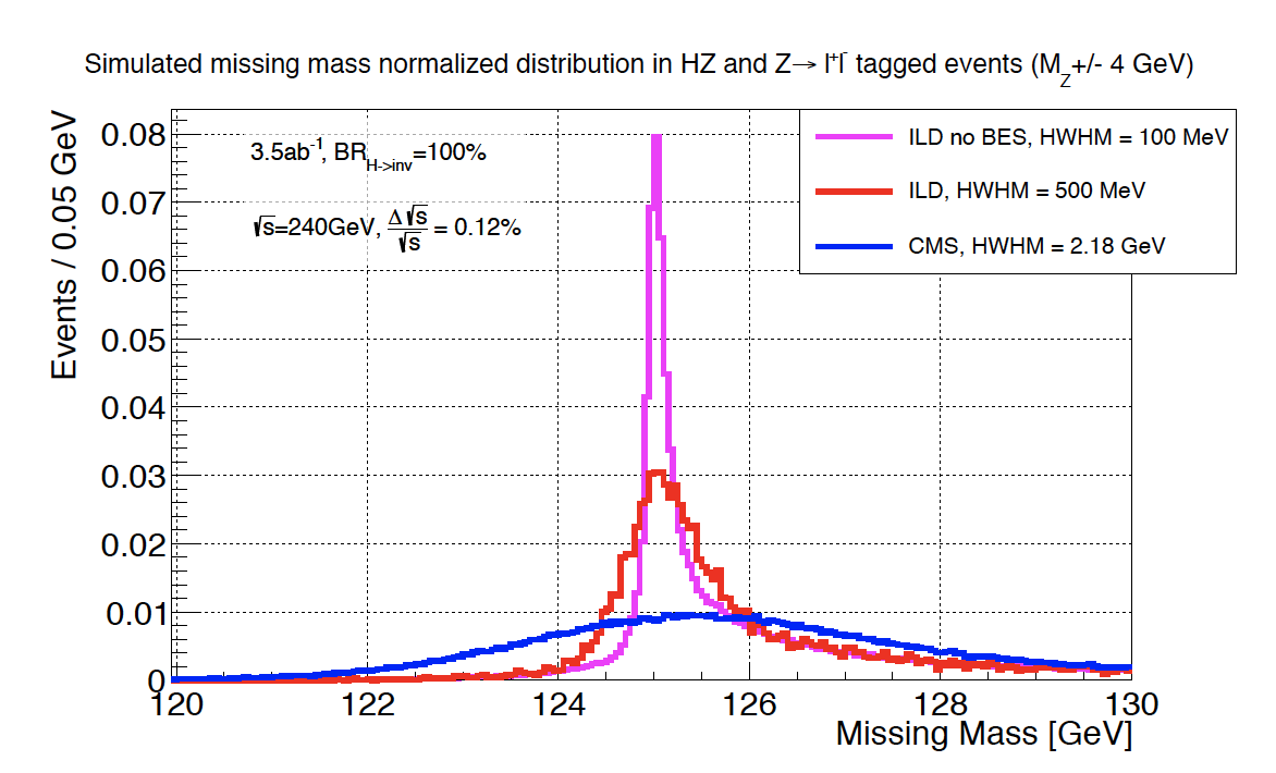
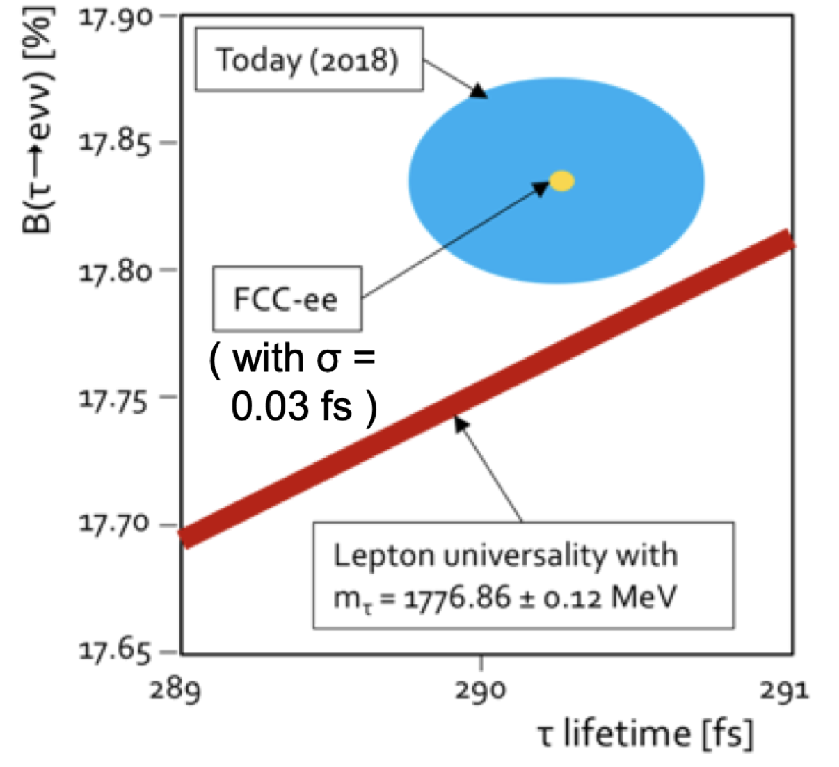
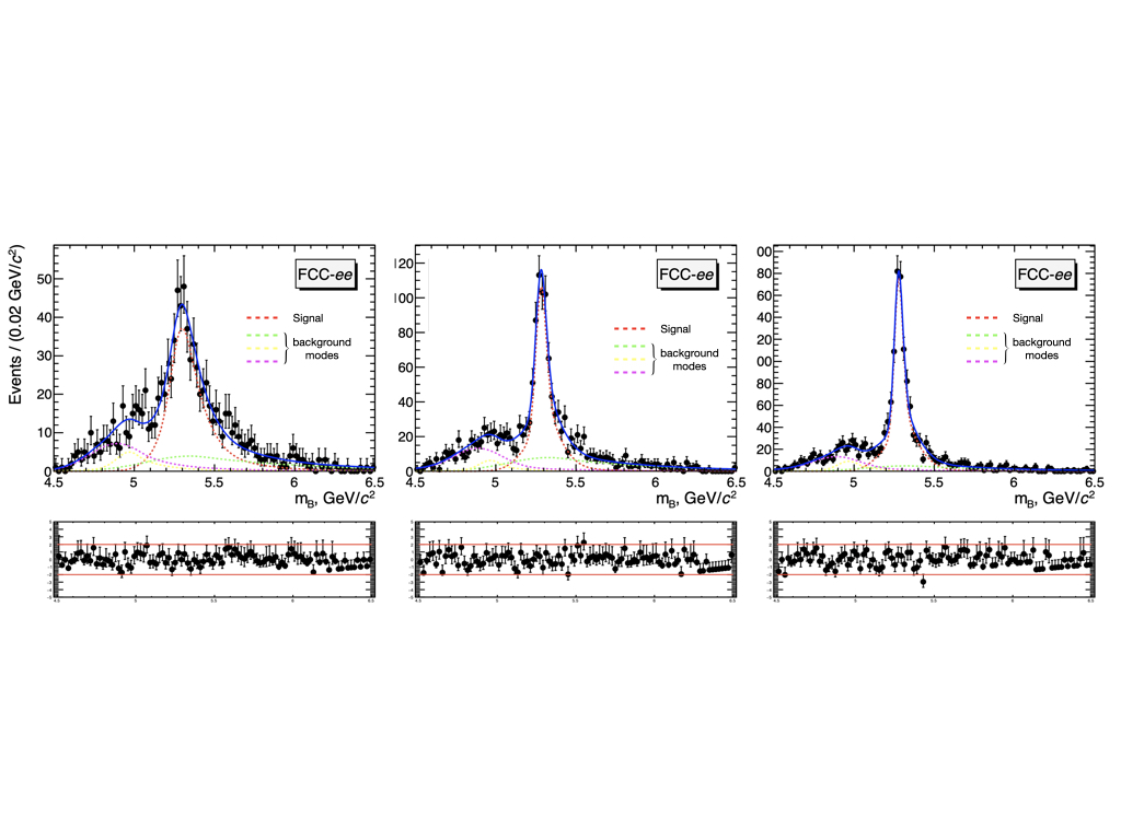
Accessing properties at the so called “TeraZ”, referring to the expected datasample of collected Z bosons, will be another major opportunity at FCC-ee 10.21468/Dam:tau . Measurements which require excellent vertexing include the lifetime, mass, leptonic branching fraction and lepton flavour violating decays such as or . The impact of improved lifetime measurements is illustrated in Fig. 1. In addition, b hadron decays modes with leptons are a crucial factor in the elucidation of flavour physics models. Examples of b-hadron decay modes which access lepton universality tests are and . is an example of a particularly interesting electroweak-penguin mode, especially in the light of current anomalies lhcbnature . The impact of the vertex detector performance for this channel is illustrated in Fig. 2.
-
•
The dramatic expected improvement in precision on the measurement of electroweak observables which can be expected at FCC-ee relies on precision tracking and flavour tagging down to low angle acceptance. This is particularly true of the b-quark electroweak measurements and , where statistical improvements by a factor 800 and 2000 are expected R1overview
-
•
The tracking system may also have an important role to play in particle identification, through dE/dx methods in the tracker, or with the addition of a tracking timing layer for time of flight measurements at the outside of the tracker (see also Section 2.2.1).
In order to address these challenges, the tracking system should satisfy the following requirements:
-
•
Acceptance
The FCC-ee will operate with low emittance beams colliding with a crossing angle of 30 mrad. These parameters define the machine-detector interface, which covers a region of 100 mrad around the detector axis. They also place a limit on the detector solenoid strength, which must be limited to 2 T machineinterface to avoid unwanted beam emittance blow-up. This has the consequence that the tracking volume must be larger than perhaps desirable, and the calorimeter may have to move outside a thin solenoid Ilardi:2021ntv . The vertexing and tracking performance must be maintained across this full acceptance to exploit the full physics potential. In addition, the angular acceptance boundaries must be defined with great accuracy, of the order of 5-10 rad, for the high precision cross-section measurements.
-
•
Occupancy and Readout
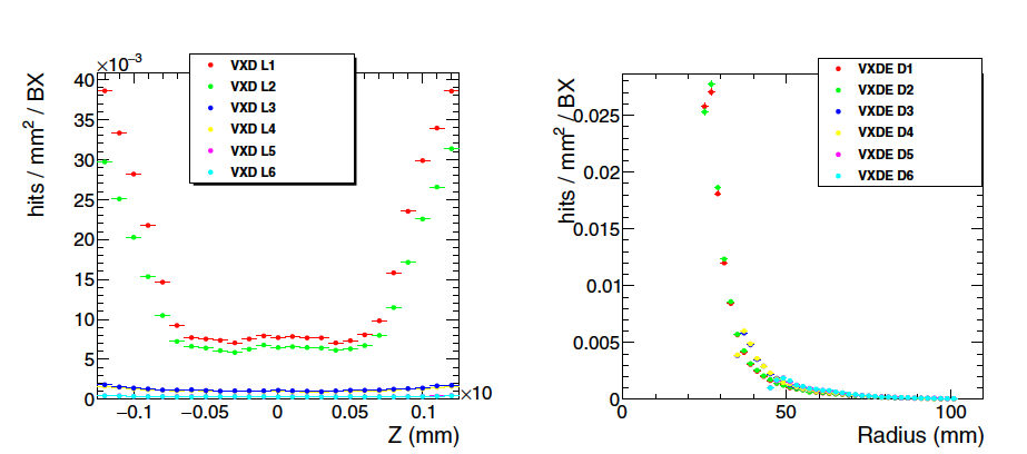
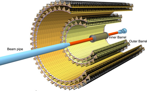
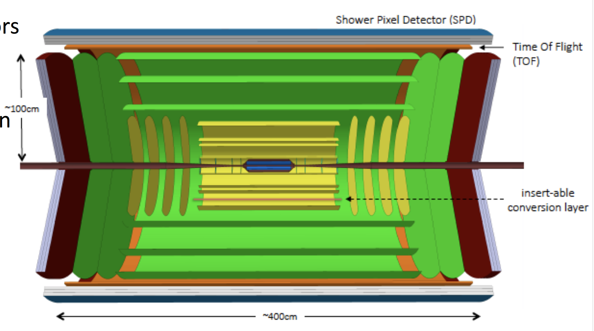
The detector readout and the front end pile up in the pixels must be able to cope with sustained physics rates of up to 100 kHz and backgrounds driven by synchrotron radiation and incoherent pair production. At 365 GeV operation, when the beams are separated by 994 ns, the occupancies in the barrel vertex detector, illustrated in Fig. 3, can reach 0.04 hits per mm2 per bunch crossing at the innermost layer. Taking into account an expected pixel pitch of approximately 25m, a cluster multiplicity of 5 and a safety factor of 3 gives an occupancy of the vertex detector still below the level of . Operating at the Z, the backgrounds are lower, however the bunch separation of 20 ns combined with an expected detector time integration window of around 1 s yields similar occupancies fcceecdr . Unlike detector designs for the ILC Behnke:2013lya , the operation cannot be in a power pulsed mode.
-
•
Impact Parameter Resolution
The target impact parameter resolution for individual tracks is ) , where is the track transverse momentum in GeV/. Both the asymptotic and multiple scattering term in this formula are crucial for FCC-ee physics. The transverse momentum of, for instance, muons from Z decays rely on the asymptotic term, whereas, tracks from, for instance the for the channel illustrated in Fig. 2 have typical transverse momenta of 3-4 GeV. This resolution results in typical primary and secondary vertex resolutions (both transverse and longitudinal) of 3 and 7 Monteil:2778908 . The system must be designed to ensure that the radial dimension can be calibrated to a relative precision of a few ppm, to ensure the same relative precision on e.g. the lepton lifetime and other weakly decaying particles.
-
•
Momentum Resolution
Excellent momentum resolution is required, with a target of , driven by the requirements for precise recoil mass reconstruction, measurements of the Higgs mass, cross sections and branching ratios. The possibility of constraining the possible point-to-point centre-of-mass energy uncertainties using the final state momentum distribution requires a high stability of the momentum scale Blondel:2019jmp ; this will require a precise and continuous monitoring of both the tracker alignment and of the magnetic field.
-
•
Angular Resolution
The typical muon angular resolution of the FCC-ee and other detectors, of the order of 0.1 mrad, is sufficient to have an impact of smaller than 1 MeV on the centre-of-mass energy determination, and can be measured with di-muon events with a more-than-adequate precision over the whole acceptance. Blondel:2019jmp
-
•
Timing measurements
Timing may be exploited in the tracking system to support PID, measurement of long lived particles, and to aid pattern reconstruction. The vertex detector may be able to use the timing information to distinguish between early and late collisions from the beam bunches, exploiting the crossing angle. This would allow a check of beam-beam systematic uncertainty and a check on . The possibility may exist to run a chromatisation scheme at the Higgs telnov2020monochromatization to scan a Higgs resonance within a single run. For these kinds of physics goals the target track timing measurement would be of the order of 6 ps.
In order to achieve these goals the target material budget for the innermost layer of the vertex detector must be or better, with a target of less than for the whole vertex detector, and the individual hit resolution must be of the order of 3 . The tracking power budget, which typically targets 40 mW/cm2 or below, and cooling mechanism must be optimised to support the best possible transparency. In addition, the tremendous statistics expected at FCC-ee will place unprecedented requirements on the stability, alignment, and calibration procedures for such a detector. To give an example, the lifetime measurement, which will allow a precise test of lepton universality, will be based on pairs and will reach an expected statistical precision of 0.001 fs, corresponding to a few tens of nanometers on the flight distance. This will set stringent requirements on the offline alignment and overall radial scale of the vertex detector.
2 Existing Detector Concepts
2.1 Tracking as implemented in the CLD concept
The CLD detector concept Bacchetta:2019fmz is an adaptation of a CLIC style detector design Linssen:2012hp to the FCC-ee environment, especially concerning the reduced value of the magnetic field which forces the tracking region to be extended from 1.5 m to 2.1 m. Another important change is the introduction of CO2 evaporative cooling system as the pulsed power concept cannot be applied to FCC-ee. It is based on a full silicon concept with double layers of sensors on a common supporting carbon fibre structure for full coverage. It comprises 3 double layers of silicon pixel sensors and 3 double disks for the Vertex Detector, 3 double layers of short strips sensors and 7 forward double disks for the innermost tracking volume and a further 3 double layers and 4 double disks for the outer tracking volume. The vertex detector features sensors with 25 25 m2 pixels, an effective thickness of 50 m, an estimated total radiation length including cooling of 0.3 per single layer, and a total active area of about 0.35 m2. For the tracking region the proposed sensor is 200 m thick with 50 m 1 mm to 10 mm long strips with the innermost double disk pixelated, similarly to the vertex detector. The estimated radiation length is 1 per layer for the region of the sensors, coolant and mechanical structure, and a further 2.5% for the main cooling distribution pipes, main mechanical supports and cables. The total active area is about 196 m2. The total estimated tracker material budget is shown in Fig. 4.
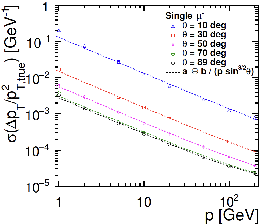
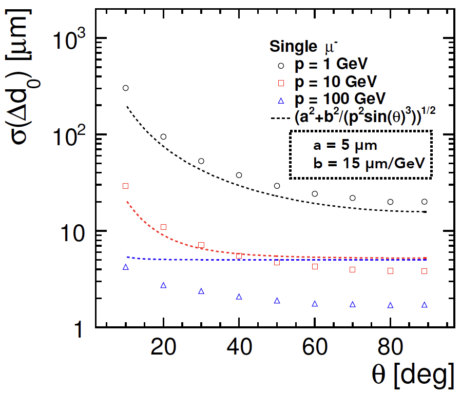
As an example of the overall performance, Fig. 5 demonstrates a resolution better than GeV-1 for 45 GeV muons at normal incidence corresponding to the required accuracy for the expected Z width measurement, and an impact-parameter resolution obtained for isolated muon tracks at various momenta achieving a resolution well below the high-momentum limit of 5 m at all polar angles.
2.2 Tracking as implemented in the IDEA concept
The current design of the IDEA detector concept Antonello:2020tzq features a silicon based vertex detector Pancheri_2019 surrounded by a large drift chamber. The vertex detector currently considered is based on active monolithic pixel sensor technology relying on fully depleted high-resistivity substrates together with on-pixel sparsification and data-driven, time-stamped readout scheme. The target performance would be a resolution of a few microns with a total material of 0.15 - 0.3 X0 per layer and power dissipation around 20 mW/cm2 in order to avoid the need for active cooling.
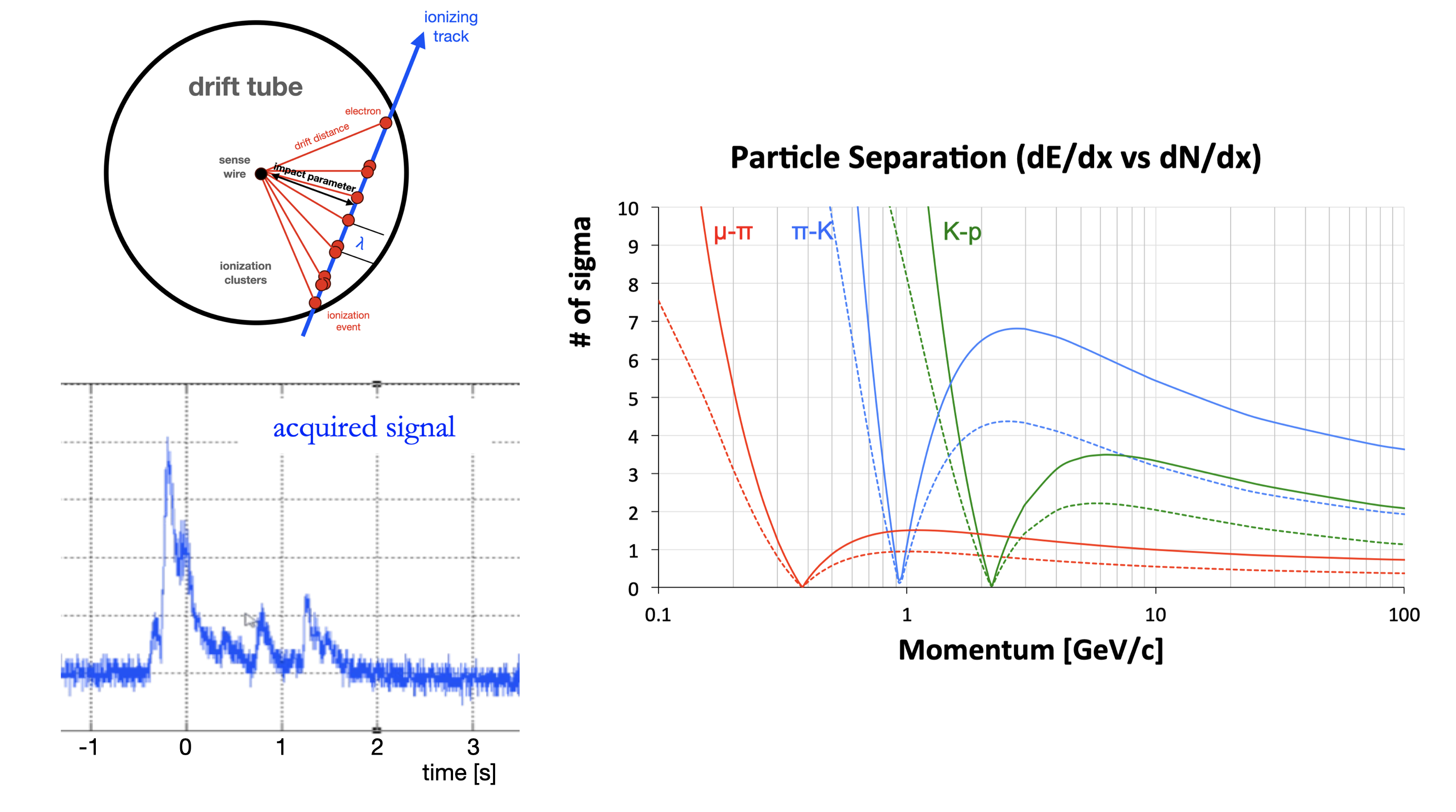
A central aspect of the IDEA detector concept is a very light central drift chamber, which should achieve lower mass than the equivalent silicon-based tracking and provide better momentum resolution over the range of interest. A novel feature of this detector is that adding timing information to the wires creates the possibility to count individual ionising events of the traversing track and dE/dx information. This is called the cluster counting method and provides PID over most of the momentum range.
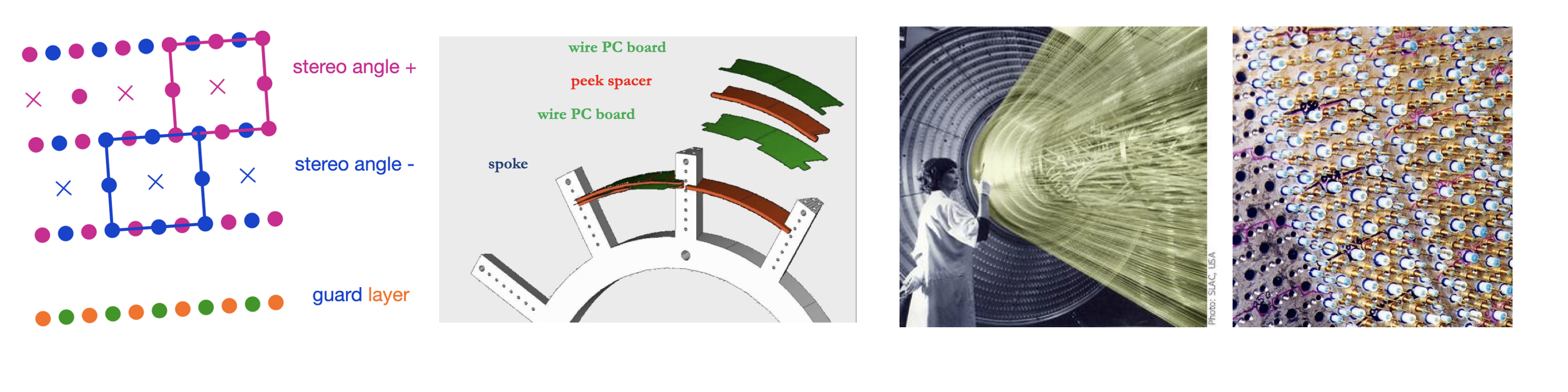
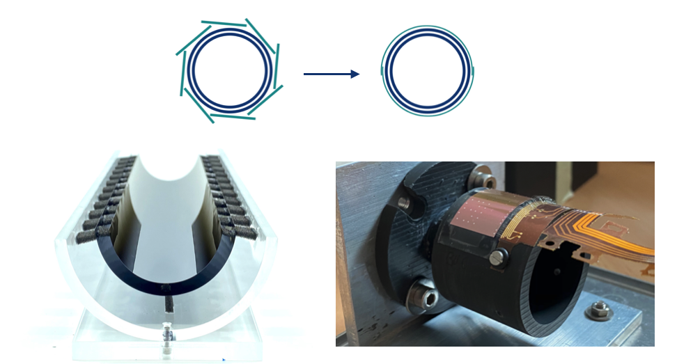
The IDEA full stereo, high resolution, ultra-light drift chamber is inspired by the MEGII drift chamber concept meg2 and its predecessors, such as the Mu2e I-tracker Pezzullo:2018rso . The wires are laid out in a way which enmeshes the positive and negative stereo angle orientations, giving a high ratio of field to sense wires, and a high density of wires creating a more uniform equipotential surface. There are almost 400k wires in total, requiring a non standard wiring procedure and a feed-through-less wiring system. The wire support endplates also serve to contain the gas, allowing a reduction of material to approximation for the inner cylinder and a few times for the endplates. The wiring technique is illustrated in Fig. 6, which shows how the wire PC board layers in green are built up on the frame, separated by precisely machined peek spacers. The cluster counting exploits the fact that in He based gas mixtures the signals from each ionisation event are spread in time over a few ns. With the help of a fast read-out electronics they can be efficiently identified and counted, giving a particle identification method with a better resolution than the integrated dE/dx method.
2.2.1 IDEA - Silicon wrapper
The IDEA silicon wrapper offers a precise track 3D position measurement at the particles’ exit point from the central drift chamber. It opens the possibility to provide an absolute reference for the calibration of the polar angle measurement, and hence define precisely the angular acceptance. The wrapper encapsulates the tracker in both the barrel and forward regions. In addition, if the silicon provides timing information this can can complement the PID range missing from IDEA by providing a time of flight detector. For instance, to cover the pion/kaon loss of discimination around 1 GeV, a timing of 0.5 ns at 2 m just outside the drift chamber would be sufficient to recover the performance. An improved time resolution could strengthen the PID up to 5 GeV. Such a timing measurement will also be valuable for the reconstruction of secondary vertices in the search, or discovery, of massive long lived particles.
3 Future Tracking Technologies
In the rest of this document we focus on silicon based tracking devices and possible technological solutions which can be appropriate for FCC-ee implementation. The IDEA concept described above is an example of a state of the art gaseous tracking solution, a full discussion of gaseous based alternatives lies outside the scope of this article.
3.1 Silicon based tracking devices
Silicon strips and pixels are currently the work horses of the vertexing and tracking programmes of the LHC experiments, and the current R&D directions show excellent potential for addressing the needs of the vertex detector, optionally the tracker, and any external or timing layers of the tracking region of an FCC-ee detector. Traditionally we distinguish two major categories of pixelated silicon tracking systems, hybrid and monolithic detectors. In the hybrid system the sensor and front end chip are optimised separately and a fine pitch bump bonding technology is used to connect the sensor with the readout chip. For monolithic devices the charge generation is integrated directly into the ASIC saving on the cost and complexity of the bump bonding step and allowing extremely thin sensors produced in a commercial process, suitable for the vertex region of an FCC detector. However, new technologies such as TSVs, microbumps, wafer stacking as well as alternative interconnection technologies blur the distinction between purely hybrid and monolithic approaches and will offer excellent potential for optimised devices for the future.
Figure 8 presents an overview of several variants of hybrid and monolithic pixel developments.
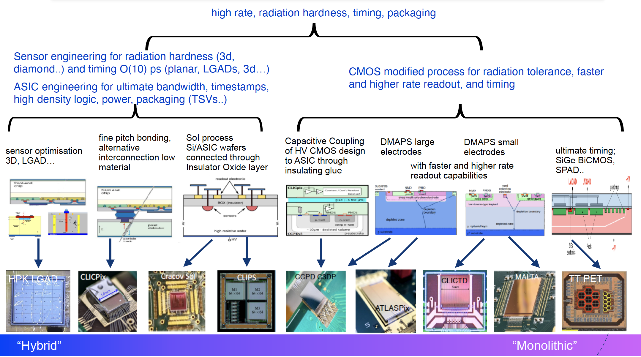
3.2 Monolithic CMOS MAPS
The recent developments of low mass and low power CMOS MAPS (Monolithic Active Pixel Sensors) combined with the possibilities of large area coverage make this a very interesting technology option for FCC-ee. In recent years commercial CMOS processes with quadruple-well technologies to allow for full CMOS circuitry inside the pixel cell as well as high resistivity substrate wafers to enable depleting part or the full sensing volume have become available and are being explored by a large community.
The current state of the art in terms of installed detectors is represented by the upgrade of the ALICE ITS during LS2, which is the largest CMOS MAPS tracking detector ever built ( 10 ). This tracker has been installed in the ALICE experiment and is currently being commissioned. The ALPIDE sensors are built in a commercial 180 nm imaging process and feature pixels. The innermost three layers of this 7 layer tracker are constructed with a material budget of 0.35 using 50 m thin MAPS connected to an Aluminium based flex cable and mounted on a low material budget mechanical support and cooling structure. The ALPIDE use a high resistivity epitaxial layer as a sensing volume on top of a low resistivity p-type substrate. By applying a moderate reverse bias ( 6V) the sensing volume around the collection electrode ( 3 m diameter) can be partially depleted. This is fully compatible with operation in the ALICE radiation environment with total ionizing doses of Mrad and NIEL fluences of 2 1013 1 MeV neq cm2. During Pb-Pb collisions with an interaction rate of 50 kHz all events will be read out, while during p-p collisions the readout will be 400 kHz. The ALPIDE chip is a monolithic pixel chip with a small collection electrode, thus optimising the analogue power consumption. Together with a sparsified asynchronous readout without distribution of the clock to the matrix, power densities of about 300 mW/cm2 for the innermost layers can be achieved, meeting the ALICE readout requirements.
HVCMOS sensors use commercial processes that embed NMOS and PMOS transistors in a single deep n-well that acts as a charge collection electrode peric . This allows to bias the substrate with a high negative voltage and to deplete the zone around the n-well. This technology has been chosen for the Mu3e experiment mu3e which has very stringent constraints on the material budget and requires the sensors to be thinned to 50 m. The 2 2 cm2 large sensors are mounted on a low mass service flexible printed circuit. The pixel detector is operated inside a dry helium atmosphere cooled by helium gas flow to further reduce multiple scattering mu3e .
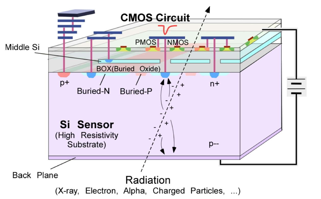
The next generation monolithic sensors are moving in the direction of Depleted MAPS (DMAPS) driven by requirements for radiation hardness and faster readout as well as fast timing information. These sensors are built from high resistivity substrates and aim to deplete the sensing volume by applying few tens to several hundred volts reverse bias. By fully depleting the sensing volume the charges generated by a passing particle are collected by drift and not dominated by diffusion, which leads to longer charge collection times and potential charge trapping and loss in case of high radiation environments. Furthermore, fast charge collection by drift also improves the signal timing information. Several different design approaches are being studied for DMAPS, which can be coarsely divided into so called “small electrode” and “large electrode” designs, see also Fig. 9.
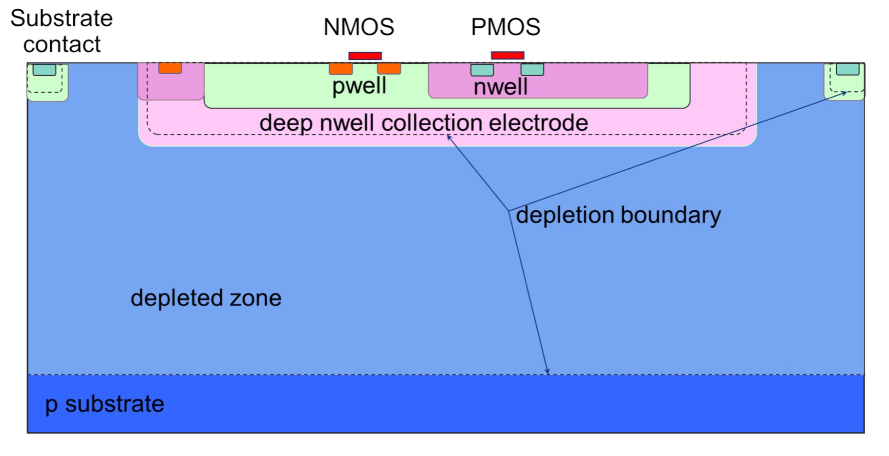
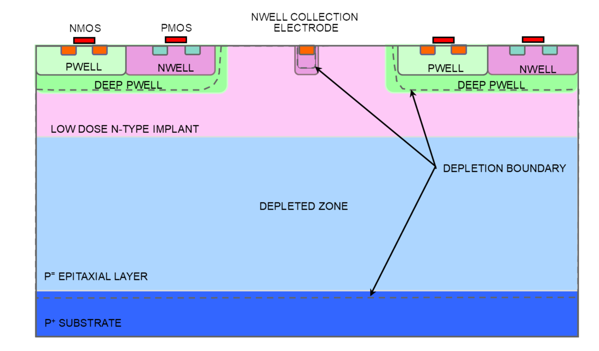
The small electrode approach with typical collection electrode diameters of a few microns seems especially promising, as it presents a much lower capacitance (a few fF as opposed to values greater than 100fF), allows for implementation of smaller pixels in the same technology node, delivers faster signals, and a potential of better signal to noise and lower analogue power. This combined with a sparsified asynchronous readout scheme allows the reduction of the power density of the chip, however is dependent on the hit rate. Challenges of this approach include the routing of the signals to the chip periphery and will depend on the technology chosen and the feature size of it. Some of these concepts have already been incorporated in ASICs such as the MALTA/Monopix chip SNOEYS201790 implemented in a modified Tower Jazz 180 nm process, and optimised for radiation hardness and speed hsdt_pernegger , and were also included in the CLICTD sensor chip kremastiotis2020clictd , optimised for extended efficiency for ultra thin silicon trackers.
The MALTA chip is now being explored using high resistivity Cz silicon to enable high depletion depth maltacz , potentially using the full wafer thickness to increase the number of charges created by a passing particle while ensuring full depletion and fast charge collection by drift. These recent developments are proving that the area of sensor engineering, traditionally associated with hybrid pixel detectors, applies also to the monolithic domain. It opens up possibilities to engineer substrates and designs with improved charge collection properties and timing information.
Moving to a smaller feature size should allow smaller pitch as well as more room for routing and more functionality to be included in the pixel. Presently, several technology nodes with smaller feature sizes EPRD , ecfaTF7 are being explored. Adding further information on the charge deposited in the pixel cells and thus moving beyond a pure binary readout will help improving the hit resolution, while keeping in mind the available power budget.
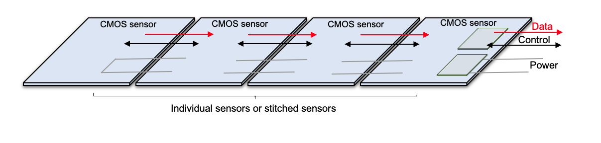
ALICE is already looking beyond the ITS for an ultra light inner barrel detector which could be installed in LS3. This would consist of a new beam pipe with inner radius 16 mm and sensing layers based on ultra thin, wafer scale sensors which can directly be curved to the required shape and operated with air cooling. The application of such a self supported, curved circuit to FCC-ee would allow a decrease in average radius and would eliminate overlaps, acceptance loss and systematic effects due to varying radius or material from supports and services. It is made possible by the industrial availability of stitching which allows multi-reticle size ladders to be constructed of up to 30 cm in 65 nm, together with the ability to thin the sensors to 20-40 m giving ultra thin and light detectors together with mechanical flexibility. ALICE aims to exploit this process for a curved inner detector beyond LS3, and subsequently to construct an all silicon tracker for beyond LS4 operation consisting of 100 double sided and curved layers. First test structures using stitching have been submitted for fabrication. While imaging sensors already use stitching to achieve large wafer scale sensors ral , ral2 , the application in HEP environments is now emerging and under study.
The challenges of such a design include the connection between the chips on the module level as well as off-module. The first connections to a curved sensor have been achieved successfully using aluminium wedge wirebonding, as shown in Fig. 11. The curved sensor with bending radius of 1.8 cm is mounted on a special jig for wire bonding; even at this radius the surface presented to the bonding machine for a given pad is essentially flat and the bonding can be completed successfully. To connect the sensor over the full width of 3 cm, the jig has to be rotated to always present a flat bonding surface for the bonding head.
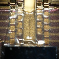
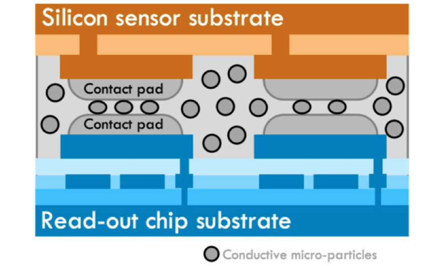
The study of alternative interconnection technologies beyond the traditionally used aluminium wedge wire bonding focuses on building large area modules with reduced and optimised interconnection schemes EPRD . This includes data and power transfer from chip to chip, as implemented in the MALTA chip, as well as the study of connection off-module. ACF (Anisotropic Conductive Film) is here a promising candidate to achieve a low mass, simplified connected between chip pads and a flexible printed circuit. Figure 12 shows ACF film deposited on two MALTA chips before flip chip connecting a silicon bridge that connects the data and power pads from one chip with the neighbouring chip ACF . The data accumulated in one chip will be transferred via the bridge contact to the neighbouring chip, merged with the data of the second chip and read out. This concept it presently under study to be extended to four MALTA chips, where the data from all chips are read out only via the last chip in the chain. This technique can also be used for serial powering and thus reducing the material budget for services. Due to the pad size of 88 m side length the connections between chips is presently carried out using either the silicon bridge or aluminium wedge wire bonding modules .
Further studies, such as the use of RDLs (ReDistribution Layers) will allow the scaling of the chip pad connectivity with the typical size of flexible printed circuit pads, so that assembly techniques can be simplified for larger module numbers and thus larger surfaces, see schematic sketch in Fig. 13.
3.3 DEPFET, FPCCD technologies
The DEPFET and FPCCD technologies are examples of sensors with a split charge amplification and readout scheme. Each pixel is a p channel FET on a fully depleted bulk; the electrons are stored in the internal gate, and the accumulated charge is removed after readout by a clear contact. After processing the wafer backside may have deep areas removed via anisotropic deep etching - the sensors are supported by the monolithically integrated silicon frame and the thickness of the sensitive area is almost a free parameter. This has allowed the DEPFET pixel detector at Belle II to be constructed with a record 0.2 per layer. The next generation of DEPFET detectors will further optimise the shape of the drain implants to improve the signal, reduce the power consumption, and improve the radiation hardness BORONAT2016982 , and in a similar way to the MAPS developments, curved sensors might be employed.
FPCCDs offer the the possibility to achieve very small pixels, 5 m square, with a sensitive layer that is fully depleted. The signal charge is transferred over a longer distance, up to a few cm, which can lead to radiation induced charge transfer inefficiencies. While radiation damage induced defects cause charge loss by trapping, several techniques to compensate this effect are under study. Using so called fat-zero charge injection methods which fill the radiation induced lattice defects are being investigated. Furthermore, notch-CDD designs that optimise the charge transfer channel width from one pixel to another as well as operation at low temperature are employed to reduce the radiation induced charge transfer inefficiencies fpccd .
3.4 3D Integration, SoI
Industrial developments are strongly focused on heterogenous integration technologies which will allow further reductions in cost and power over the coming years. Several of these technologies, such as 3D stacking are also been studied for future HEP applicationsecfa_roadmap ; pristauz . The developments in this area are dependent on availability of processes for R&D activities, but are a very promising path for future developments which will increase the functionality and performance of silicon trackers.
The developments of SOI (Silicon On Insulator) detectors present a two-tiered separation of the readout electronics and the sensing layer Tsuboyama:2019gzj . An SOI wafer with a high resistivity sensor part is connected to a thin CMOS chip using oxide bonding. Figure 14 shows a schematic SOI structure indicating the different tiers and signal generation by a passing particle. This approach has been further developed using buried wells, double SOI and pinned depleted diodes to address signal cross talk and radiation tolerance Arai:2017dni .
3.5 Solutions based on hybrid pixel sensors
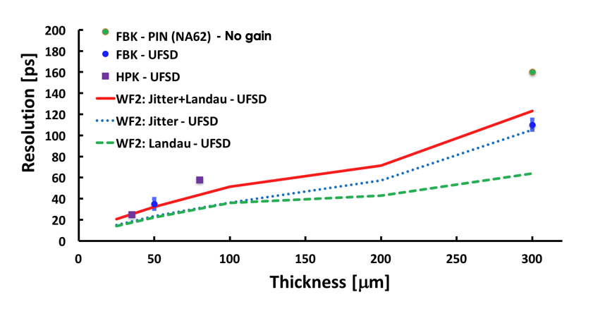
Hybrid pixel solutions, which make up the majority of currently installed systems, offer the possibility to separately optimise the sensor characteristics while being able to benefit from standard commercial processes for a high degree of functionality for the ASIC. They are typically able to cope with very high rates and high radiation environments. Challenges include reducing the material for the sensor, ASIC and interconnection region, and the costs and technological challenges of fine pitch bump bonding. The hybrid pixel solution is of particular interest for FCC-ee due to the possibility of adding sensor and ASIC timing capability, which could be exploited in external layers or in the wrapper layer to support PID capability. A candidate sensor technology for fast time stamp applications is that of LGADs (Low-Gain Avalanche Diodes hartmut ) which incorporate a thin multiplication layer which aims to supply a small gain which is sufficient to give a reliable timing signal. Such a technology has been shown to be capable of delivering 20 ps resolution or better, depending on the signal size and sensor thickness KRAMBERGER201926 . The concept of a timing layer using LGADs is being exploited for both the ATLAS and CMS upgrade timing layers in the endcap regions, which aim for a system level timing resolution of 30 ps with 10-15 m2 of silicon, for installation in 2023-2025 Butler:2055167 ; CERN-LHCC-2015-020 ; Mazza:2019dkn ; Lazarovits:2020nfz . The LGAD technology is being improved to allow a fine pitch pixel readout, which in traditional LGAD designs is impeded by the no-gain region between the pixels. This can be addressed with solutions such as using trenches for pad isolation, the so-called TI-LGAD paternoster , moving the gain region to the other side of the sensor (“iLGAD - inverted LGADs cartiglia_ilgad ”) or implementing a resistive readout solution, the so-called AC-LGAD or RSD, which can achieve excellent position resolution even with large pixels, freeing up space in the ASIC to allow timing functionality to be added tomago . An alternative approach could be monolithic BiCMOS, exploiting the properties of SiGe transistors, where the development is now beginning, and where the timing performance could also be enhanced with the use of internal gain.
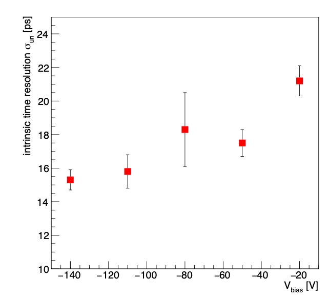
A further possibility for timing detectors which do not incorporate internal gain is the use of silicon sensors with a three dimensional (3-D) architecture PARKER1997328 , where the n and p electrodes penetrate fully or partially through the silicon substrate. This is a rapidly evolving technology which was first successfully deployed at the LHC for the ATLAS IBL DaVia:2012ay and is currently being evaluated for the Phase II LHC Upgrades SZUMLAK2020162187 . Due to the inherently short drift distance, independent of the sensor thickness, the 3D sensors can be very fast, and have good radiation tolerance, and low operation voltages and power dissipation. One of the challenges for timing resolution comes from the variations in the weighting field due to the hit position, and the fill factor, which may be significant for small cell sizes and certain track inclinations. One way to tackle the weighting field variations is with a trench design, as developed by the TIMESPOT collaboration, and for which intrinsic detector resolutions of the order of 10 ps have been demonstrated in testbeam, as shown in Fig. 15 (right). An implementation of timing sensors in a wrapper layer for FCC-ee, with relaxed requirements on pitch may be able to benefit from the enhanced time resolution of traditional column 3D sensors in a configuration with multiple cells connected together kramberger_timing .
The development of any sensor with timing capability must be done hand in hand with the accompanying IC technology. Applications at FCC-ee can expect to benefit from the current ongoing RD into ASIC developments for HEP applications including LHC Upgrades, as well as imaging applications. Recent developments include the Timepix4 ASIC timepix4 , a full size 4-side tileable chip with high rate imaging capabilities which has been successfully developed in 65 nm CMOS technology and provides a time stamp binning resolution of 195 ps (RMS 56 ps). The Timespot demonstrator ASIC TimeSpOT:2020gln , is being developed in 28 nm CMOS technology and aims for ultimate time resolution using a CSA inverter input stage. The LHCb experiment plans a Phase II Upgrade lhcbupgrade2 , due for installation after LS4, which will require a high granularity pixel vertex detector capable of hit timestamps, operating at high speed in a high radiation environment. Such developments provide a promising path forward for an eventual hybrid pixel layer implementation at FCC-ee.
3.6 Mechanical Integration and Interconnection Technologies
3.6.1 Mechanics and Cooling
The Cooling and mechanical design of a FCC-ee tracker poses many challenges. In order to benefit from progress towards very thin sensors, the supports and services must also reduce the amount of mass and the detector must benefit from an integrated design. The very high luminosities and cross section at the Z peak imply relative experimental systematic uncertainties at the level, required to match the statistical accuracies. Hence mechanical stability is also a crucial consideration, whether deviations come from internal effects such as vibrations or thermal effects, or external stimuli such as cavern floor movements, earthquakes or stress from other subsystems.
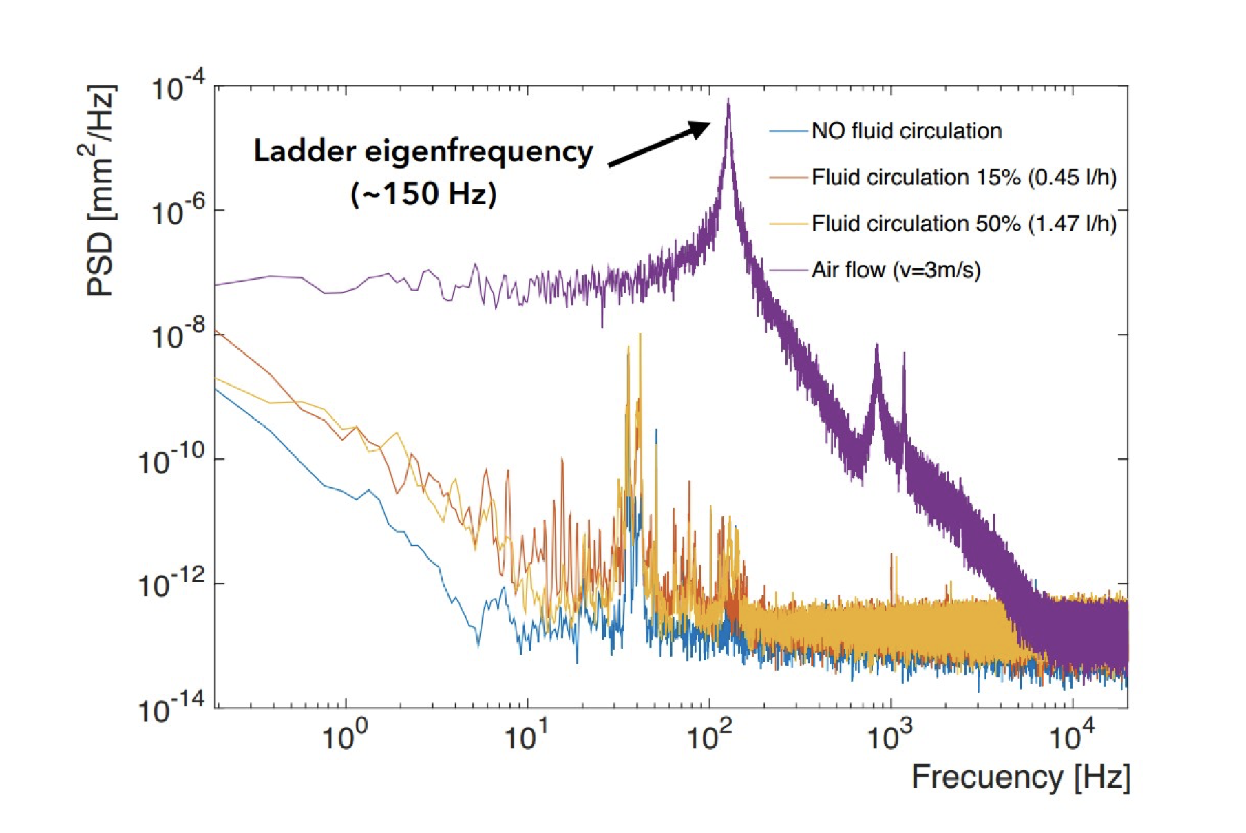
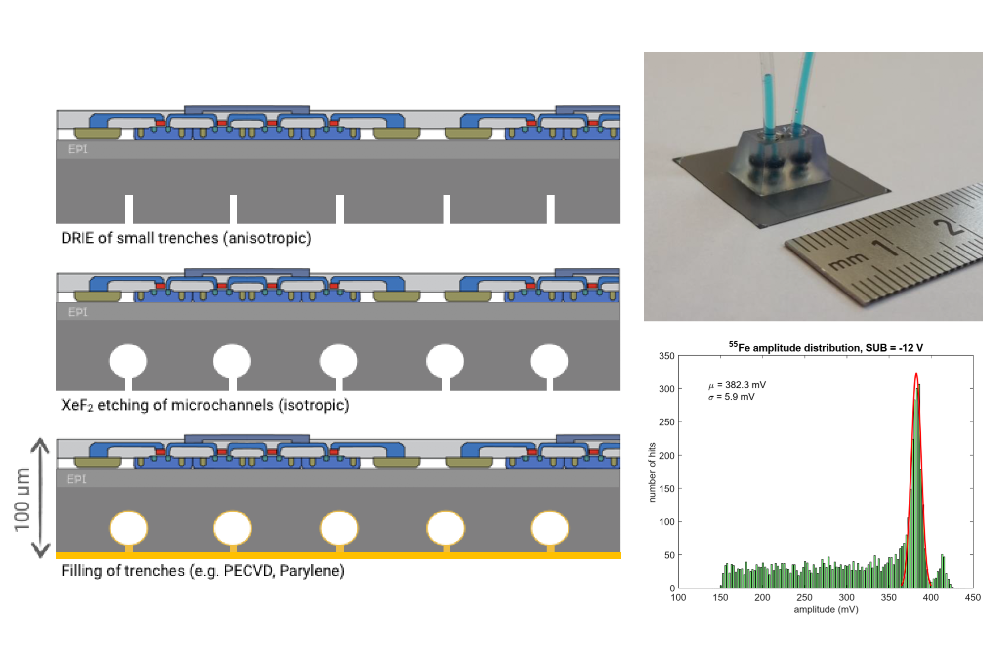
The global design of the FCC-ee tracker will need to take advantage of the lightweight next generation solutions for the mechanical supports and cooling. In the ideal case the detector active cooling circuits are completely removed and the heat is removed by a forced airflow. In this case attention must be paid to the vibrations which can be induced in thin silicon ladders. The design must be backed with simulations and realistic mechanical measurements Viehhauser_2015 . An example of such a study is shown in Fig. 16. This approach is currently under investigation for the ALICE ITS3 alicetdr ; magnus , where the stitched, curved sensors are supported by ultra-light carbon foam supports which also act as radiators, and the whole device is contained within an external carbon exoskeleton. The engineering model is currently being tested in a wind tunnel for thermal and mechanical stability. It may be that air cooling cannot be implemented, if for instance there are regions with more dense power consumption, or if the size and complexity of the detector does not allow large quantities of air to be introduced in well controlled temperature conditions. If a small increase in material budget is acceptable, microchannel cooling lhcbuchan represents one very promising area of development. Such a solution has already been implemented for the LHCb pixel detector upgrade, where the coolant is evaporative CO2 which circulates in tiny microchannels embedded within a cooling plate consisting of a silicon wafer. Such a system has the advantage of a low and uniform mass distribution, a high thermal efficiency, a good CTE match between substrate and sensor, and a flexible geometry allowing the coolant to be brought precisely below the needed regions. A low material contribution is possible, for instance in the case of the GTK microchannel cooling plates of the NA62 experiment na62uchan , which are thinned in the acceptance to a final contribution of 0.13% X0. Recent technological advances for the silicon etched microchannel solution allow the cooling channels to be directly integrated in the sensor substrate. This has been demonstrated for instance in the buried channel process developed by FBK which has been demonstrated on a single MALTA die to be compatible with the CMOS processing Mapellivci and showing full functionality. Similarly, integrated micro-channel cooling to DEPFET detectors is also under consideration Vos:2017uin . For future microchannel applications a variety of processes in additive manufacturing are being considered. These allow in principle a large choice of materials such as metals, ceramics or acrylics, and have the advantage great flexibility in the geometric forms, as well as being able to address the issue of the interconnections, where for the etched silicon solution the connections tend to be more bulky and fragile. A similar approach is taken by the concept of a microvascular network embedded in a carbon cold-plate carbonvascular , which could be adapted to silicon detector cooling supports.
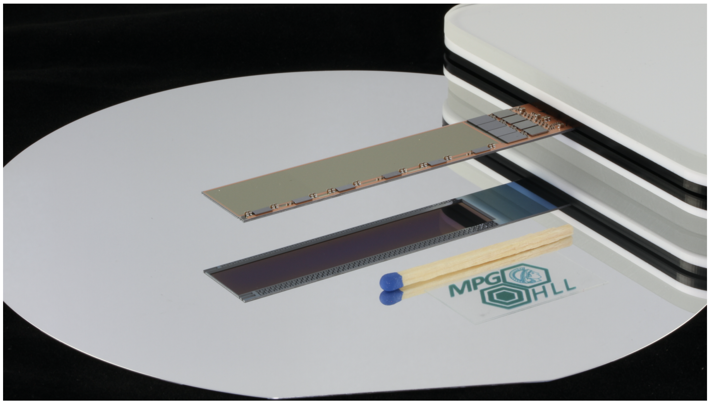
An excellent example of the integration of supports, routing and electronics in one thin all-silicon ladder detector is given by the DEPFETs of Belle II, as illustrated in Fig. 17. Whichever technological solution is chosen for a future FCC-ee detector the way in which the sensors are integrated into modules will be critical due to the need to maintain low material throughout the tracking region. The FCC-ee vertex detector will rely on enabling technologies for module packaging, including thinning and dicing techniques, fine pitch bump bonding, or design of multichip modules incorporating concepts such as serial powering.
4 Conclusions
The tracking system of a future FCC-ee detector will require innovative technological solutions for the sensors, mechanics and readout in order to address the needs for high precision and low mass. New solutions have to be found be found for alignment and field stability, so that tracker systematics match the new level of statistical accuracy. The chosen solutions must take advantage of current trends in cutting edge technology. In particular, advances in low mass, low power and fine pixel monolithic sensors may be applicable in the inner most layers, sensors with timing capability may be used in outer layers or as an outer wrapper, and the main tracking body may employ for example an all silicon solution or a low mass drift chamber. The detector will act as the interface to the machine and the design and constraints on the beampipe design must be closely integrated with the evolution of the detector layout.
References
- (1) FCC collaboration, A. Abada et al., FCC Physics Opportunities: Future Circular Collider Conceptual Design Report Volume 1, Eur. Phys. J. C 79 (2019) 474.
- (2) A. Blondel and P. Janot, FCC-ee overview: new opportunities create new challenges, in A future Higgs and Electroweak factory (FCC): Challenges towards discovery, EPJ+ special issue, Focus on FCC-ee, 2106.13885.
- (3) J. De Blas et al., Higgs Boson studies at future particle colliders, The European Physical Journal Special Topics 139 (January, 2020) .
- (4) M. Dam, Tau-lepton Physics at the FCC-ee circular e+e- Collider, SciPost Phys. Proc. (2019) 41.
- (5) LHCb collaboration, R. Aaij et al., Test of lepton universality in beauty-quark decays, accepted by Nature Physics, 2103.11769.
- (6) A. Blondel and P. Janot, “FCC-ee overview: new opportunities create new challenges.” A future Higgs and Electroweak factory (FCC): Challenges towards discovery, EPJ+ special issue, Focus on FCC-ee.
- (7) O. Cerri, M. de Gruttola, M. Pierini, A. Podo and G. Rolandi, Study the effect of beam energy spread and detector resolution on the search for Higgs boson decays to invisible particles at a future e+ e- circular collider, Eur. Phys. J. C 77 (2017) 116, [1605.00100].
- (8) S. Monteil, “FCC Design Study.” talk presented at the GDR-InF Workshop, February 02, 2018. https://indico.desy.de/event/28202/contributions/98367/.
- (9) M. Boscolo, O. Blanco-Garcia, N. Bacchetta, E. Belli, M. Benedikt, H. Burkhardt et al., Machine detector interface for the future circular collider, .
- (10) V. Ilardi, H. F. P. Silva, T. Kulenkampff, A. Dudarev, P. B. de Sousa, M. Mentink et al., Ultra-Thin Solenoid and Cryostat Development for Novel Detector Magnets, IEEE Trans. Appl. Supercond. 31 (2021) 4500205.
- (11) A. Abada, M. Abbrescia, S. S. AbdusSalam, I. Abdyukhanov, J. Abelleira Fernandez, A. Abramov et al., Fcc-ee: The lepton collider, The European Physical Journal Special Topics 228 (2019) 261–623.
- (12) H. Abramowicz et al., The International Linear Collider Technical Design Report - Volume 4: Detectors, 1306.6329.
- (13) S. Monteil and G. Wilkinson, Heavy-quark opportunities and challenges at FCC-ee. Heavy-quark opportunities and challenges at FCC-ee, Eur. Phys. J. Plus 136 (Jun, 2021) 837. 14 p, [2106.01259].
- (14) A. Blondel, P. Janot, J. Wenninger et al., Polarization and Centre-of-mass Energy Calibration at FCC-ee, 1909.12245.
- (15) V. I. Telnov, Monochromatization of colliders with a large crossing angle, 2020.
- (16) N. Bacchetta et al., CLD – A Detector Concept for the FCC-ee, 1911.12230.
- (17) L. Linssen, A. Miyamoto, M. Stanitzki, H. Weerts et al., Physics and Detectors at CLIC: CLIC Conceptual Design Report, 1202.5940.
- (18) RD-FA collaboration, M. Antonello, IDEA: A detector concept for future leptonic colliders, Nuovo Cim. C 43 (2020) 27.
- (19) L. Pancheri, J. Olave, S. Panati, A. Rivetti, F. Cossio, M. Rolo et al., A 110 nm CMOS process for fully-depleted pixel sensors, Journal of Instrumentation 14 (jun, 2019) C06016–C06016.
- (20) A. M. Baldini, E. Baracchini, C. Bemporad, F. Berg, M. Biasotti, G. Boca et al., The design of the meg ii experiment, The European Physical Journal C 78 (May, 2018) .
- (21) G. Pezzullo, The Mu2e Tracker, in 39th International Conference on High Energy Physics, 11, 2018.
- (22) I. peric et al., High-voltage pixel detectors in commercial cmos technologies for atlas, clic and mu3e experiments, Nuclear Instruments and Methods in Physics Research A 731 (2013) 131–136.
- (23) K. Arndt, H. Augustin, P. Baesso, N. Berger, F. Berg, C. Betancourt et al., Technical design of the phase i mu3e experiment, Nuclear Instruments and Methods in Physics Research Section A: Accelerators, Spectrometers, Detectors and Associated Equipment 1014 (2021) 165679.
- (24) T. Kugathasan, Review on depleted CMOS, in Proceedings of The 27th International Workshop on Vertex Detectors — PoS(VERTEX2018), vol. 348, p. 042, 2019. DOI.
- (25) W. Snoeys, G. Aglieri Rinella, H. Hillemanns, T. Kugathasan, M. Mager, L. Musa, P. Riedler, F. Reidt, J. Van Hoorne, A. Fenigstein, T. Leitner, A process modification for cmos monolithic active pixel sensors for enhanced depletion, timing performance and radiation tolerance, Nuclear Instruments and Methods in Physics Research Section A: Accelerators, Spectrometers, Detectors and Associated Equipment 871 (2017) 90–96.
- (26) H. Pernegger et al., Radiation hard monolithic CMOS sensors with small electrodes for HL-LHC, Nuclear Instruments and Methods in Physics Research A 986 (2021) .
- (27) I. Kremastiotis, R. Ballabriga, K. Dort, N. Egidos and M. Munker, Clictd: A monolithic hr-cmos sensor chip for the clic silicon tracker, 2020.
- (28) H. Pernegger et al., MALTA-Cz: A radiation hard full-size monolithic CMOS sensor with small electrodes on high-resistivity Czochralski substrate, publication in preparation (2021) .
- (29) “Strategic R&D Programme on Technologies for Future Experiments - Annual Report.” to be published, 2021.
- (30) ECFA Detector RD Roadmap Symposium of Task Force 7 Electronics and On-detector Processing, 2021.
- (31) R. G. McMullan, A.R. Faruqi, Direct electron detectors, Methods in Enzymology 579 (2016) 1–17.
- (32) R. Turchetta, N. Guerrini, I. Sedgwick, Large Area CMOS Image Sensors, Jounal of Instrumentation 6 (2011) C01099.
- (33) M.Mager, “ALICE ITS upgrade for LS3.” talk presented at the 13th Terascale Detector Workshop, 2021. https://indico.desy.de/event/24227/.
- (34) M. Vincente Baroso et al., “Pixel detector hybridization and integration with Anisotropic Conductive Films.” talk presented at the 16th Trento workshop on advanced silicon radiation detectors, 2021. https://indico.cern.ch/event/983068/contributions/4223158/.
- (35) P. Riedler et al., Studies for low mass, large area monolithic silicon pixel detector modules using the MALTA CMOS pixel chip, Nuclear Instruments and Methods in Physics Research A (2021) .
- (36) “CERN EP Detector Technologies - Annual Report.” to be published, 2021.
- (37) P.Riedler, “CMOS trackers– present and future developments.” talk presented at the ECFA R&D Roadmap Symposium of Task Force 3 - Solid State Detectors, 2021. https://indico.cern.ch/event/999816/.
- (38) M. Boronat, Depfet pixel detector for future e-e+ experiments, Nuclear and Particle Physics Proceedings 273-275 (2016) 982 – 987.
- (39) S. Murai, A. Ishikawa, T. Sanuki, A. Miyamoto, Y. Sugimoto, H. Sato et al., Radiation tolerance of FPCCD vertex detector for the ILC, in International Workshop on Future Linear Colliders, 3, 2017. 1703.05603.
- (40) P.Allport, “ECFA Detector R&D Roadmap Status.” talk presented at the EPS-HEP Conference, July 30, 2021. https://indico.cern.ch/event/686737/contributions/2818061/attachments/1594064/2523898/FCC_20180202_GDRInf_monteil.pdf .
- (41) H. Pristauz, A. Mayr and S. Behler, Disruptive developments for advanced die attach to tackle the challenges of heterogeneous integration, 05, 2018.
- (42) T. Tsuboyama et al., R&D status of SOI-based pixel detector with 3D stacking readout, Nucl. Instrum. Meth. A 924 (2019) 422–425.
- (43) Soipix collaboration, Y. Arai, SOI Monolithic pixel detector technology, PoS Vertex2016 (2017) 029.
- (44) C. N. Sadrozinski HF, Seiden A, 4D tracking with ultra-fast silicon detectors, Rep. Prog. Phys. 81(2) (2017) .
- (45) G. Kramberger, V. Cindro, D. Flores, S. Hidalgo, B. Hiti, M. Manna et al., Timing performance of small cell 3d silicon detectors, Nuclear Instruments and Methods in Physics Research Section A: Accelerators, Spectrometers, Detectors and Associated Equipment 934 (2019) 26–32.
- (46) CMS collaboration, J. Butler, D. Contardo, M. Klute, J. Mans, L. Silvestris and on behalf of the CMS Collaboration, CMS Phase II Upgrade Scope Document, tech. rep., CERN, Geneva, Sep, 2015.
- (47) ATLAS collaboration, K. Einsweiler and L. Pontecorvo, ATLAS Phase-II Upgrade Scoping Document, tech. rep., CERN, Geneva, Sep, 2015.
- (48) S. M. Mazza, A High-Granularity Timing Detector (HGTD) for the Phase-II upgrade of the ATLAS detector, JINST 14 (2019) C10028.
- (49) CMS collaboration, M. Lazarovits, Performance of CMS Endcap Precision Timing Sensors, in Workshop of QCD and Forward Physics at the the LHC, the future Electron Ion Collider and Cosmic Ray Physics, (Lawrence), University of Kansas Libraries, 9, 2020.
- (50) G. Paternoster, G. Borghi, M. Boscardin, N. Cartiglia, M. Ferrero, F. Ficorella et al., Trench-isolated low gain avalanche diodes (ti-lgads), IEEE Electron Device Letters 41 (2020) 884–887.
- (51) N. Cartiglia et al., Beam test results of a 16 ps timing system based on ultra-fast silicon detectors, Nucl. Instrum. Meth. A 850 (2017) 83–88, [1608.08681].
- (52) M. Tornago et al., Resistive AC-Coupled Silicon Detectors: principles of operation and first results from a combined analysis of beam test and laser data, Nucl. Instrum. Meth. A 1003 (2021) 165319, [2007.09528].
- (53) S. Parker, C. Kenney and J. Segal, 3d — a proposed new architecture for solid-state radiation detectors, Nuclear Instruments and Methods in Physics Research Section A: Accelerators, Spectrometers, Detectors and Associated Equipment 395 (1997) 328–343.
- (54) C. Da Via et al., 3D silicon sensors: Design, large area production and quality assurance for the ATLAS IBL pixel detector upgrade, Nucl. Instrum. Meth. A 694 (2012) 321–330.
- (55) T. Szumlak, Silicon detectors for the lhc phase-ii upgrade and beyond rd50 status report, Nuclear Instruments and Methods in Physics Research Section A: Accelerators, Spectrometers, Detectors and Associated Equipment 958 (2020) 162187.
- (56) G. Kramberger et al., Timing performance of small cell 3D silicon detectors, Nucl. Instrum. Meth. A 934 (2019) 26–32, [1901.02538].
- (57) X. Llopart, J. Alozy, R. Ballabriga, M. Campbell, R. Casanova, V. Gromov, E.H.M. Heijne, T. Poikela, E. Santin, V. Sriskaran, L. Tlustos, A. Vitkovskiy, Timepix4, a large area pixel detector readout chip which can be tiled on 4 sides providing sub-200ps timestamp binning, Submitted to Journal of Instrumentation (2021) .
- (58) TimeSpOT collaboration, L. Piccolo et al., The first ASIC prototype of a 28 nm time-space front-end electronics for real-time tracking, PoS TWEPP2019 (2020) 022.
- (59) LHCb Collaboration collaboration, Aaij, R. et al, Expression of Interest for a Phase-II LHCb Upgrade: Opportunities in flavour physics, and beyond, in the HL-LHC era, tech. rep., CERN, Geneva, Feb, 2017.
- (60) L. Anderlini, M. Aresti, A. Bizzeti, M. Boscardin, A. Cardini, G.-F. D. Betta et al., Intrinsic time resolution of 3d-trench silicon pixels for charged particle detection, Journal of Instrumentation 15 (Sep, 2020) P09029–P09029.
- (61) G. Viehhauser, Thermal management and mechanical structures for silicon detector systems, Journal of Instrumentation 10 (Sep, 2015) P09001–P09001.
- (62) ALICE collaboration, B. Abelev et al., Technical Design Report for the Upgrade of the ALICE Inner Tracking System, J. Phys. G 41 (2014) 087002.
- (63) M. Mager, Upgrade of the ALICE ITS in LS3, Proceedings of Science Vertex2019 (2019) .
- (64) O. Francisco, J. Buytaert, P. Collins, R. Dumps, M. John, A. Mapelli et al., Evaporative co 2 microchannel cooling for the lhcb velo pixel upgrade, Journal of Instrumentation 10 (05, 2015) C05014–C05014.
- (65) G. Romagnoli, D. A. Feito, B. Brunel, A. Catinaccio, J. Degrange, A. Mapelli et al., Silicon micro-fluidic cooling for NA62 GTK pixel detectors, Microelectron. Eng. 145 (2015) 133–137.
- (66) A. Mapelli, Microfabricated silicon substrates for pixel detectors assembly and thermal management a.k.a. silicon microchannel cooling plates, Nuclear Instruments and Methods in Physics Research A 958 (220) .
- (67) M. Vos, Micro-channel cooling in high energy physics, PoS Vertex2016 (2017) 037.
- (68) S. Pety, M. Tan, A. Najafi, P. Barnett, P. Geubelle and S. White, Carbon fiber composites with 2d microvascular networks for battery cooling, International Journal of Heat and Mass Transfer 115 (12, 2017) 513–522.
- (69) L. Andricek, M. Boronat, J. Fuster, I. Garcia, P. Gomis, C. Marinas et al., Integrated cooling channels in position-sensitive silicon detectors, Journal of Instrumentation 11 (jun, 2016) P06018–P06018.