Non-invasive imaging of three-dimensional integrated circuit activity using quantum defects in diamond
Abstract
The continuous scaling of semiconductor-based technologies to micron and sub-micron regimes has resulted in higher device density and lower power dissipation. Many physical phenomena such as self-heating or current leakage become significant at such scales, and mapping current densities to reveal these features is decisive for the development of modern electronics. However, advanced non-invasive technologies either offer low sensitivity or poor spatial resolution and are limited to two-dimensional spatial mapping. Here we use shallow nitrogen-vacancy centres in diamond to probe Oersted fields created by current flowing within a multi-layered integrated circuit in pre-development. We show the reconstruction of the three-dimensional components of the current density with a magnitude down to and sub-micron spatial resolution capabilities at room temperature. We also report the localisation of currents in different layers and observe anomalous current flow in an electronic chip. Further improvements using decoupling sequences and material optimisation will lead to nA-current detection at sub-micron spatial resolution. Our method provides therefore a decisive breakthrough towards three-dimensional current mapping in technologically relevant nanoscale electronics chips.
I Introduction
The rapid growth and downscaling of silicon integrated circuits (ICs) have ushered revolutions in many areas of today’s society waldrop_chips_2016 ; xu_microscale_2005 ; iwai_silicon_2002 ; riordan_crystal_2007 , such as high-speed internet berners_lee_www_1994 , in-car navigation skog_car_2009 and leadless pacemakers bhatia_leadless_2018 . However, if the semiconductor community has underpinned Moore’s law moore_cramming_2006 for over 50 years by shrinking the size of electronic components, the scaling roadmap is nearing its end waldrop_chips_2016 ; mamaluy_fundamental_2015 . Hence, next-generation technologies like autonomous driving bhargava_fully_2019 or quantum processors gambetta_ibm_2021 rely on a new strategy: three-dimensional chip architectures salahuddin_era_2018 ; debenedictis_sustaining_2017 ; lancaster_integrated_2018 . In this regard, device development, optimisation and failure analysis are severely challenged due to the absence of methods for direct visualisation of three-dimensional charge flow. This concerns particularly multi-layer chips with sub-micron feature sizes.
Most electric current imaging techniques visualise charge transport through the associated magnetic fields that pass unaffected through the materials used in semiconductor devices. One approach consists of delayering the chip to probe fields with a micro-needle wang_probing_2017 . Non-destructive current imaging can be implemented using superconducting quantum interference devices (SQUID) microscopes, but the inherent stand-off distance limits the spatial resolution to tens of micrometres fong_high-resolution_2005 . Conversely, giant magneto-resistance (GMR) microscopes provide excellent spatial resolution at the expense of much lower field sensitivities schrag_submicron_2003 ; herrera_may_res_2009 . Importantly, SQUID and GMR microscopes are only sensitive to a single magnetic field component, limiting reliable current imaging to the two-dimensional realm.
In this article, we demonstrate non-invasive current imaging in three-dimensional integrated circuit using quantum sensors at room temperature. We use nanoscale nitrogen-vacancy (NV) centres in diamond jelezko_single_2006 ; doherty_nv_2013 which offer the unique property to probe all three vectorial components of a magnetic field simultaneously balasubramanian_nanoscale_2008 ; steinert_high_2010 . Besides, NV centres operate under a wide span of external conditions batalov_low_2009 ; steinert_magnetic_2013 ; happacher_low_2021 ; liu_coherent_2019 ; lesik_magnetic_2019 , demonstrate excellent sensitivity to magnetic fields wolf_subpicotesla_2015 ; zhang_diamond_2021 and enable nanoscale spatial resolution chang_nanoscale_2017 .
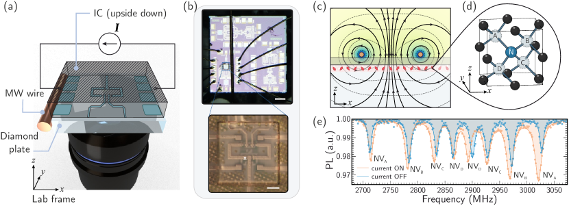
Pioneering work successfully demonstrated IC activity imaging nowodzinski_nv_2015 ; turner_magnetic_2020 but has been so far restricted to a two-dimensional study. In this work, we leap a step forward by demonstrating imaging of three-dimensional current distribution within a micro-chip used as an mm-wave test circuit for automotive radar applications. For this, we employ an NV-based wide-field microscope described in Figure 1a which allows us to synchronously map vectorial magnetic fields over a region of (see Methods). We use the instrument to measure the current density flow in the multi-layered IC (Figure 1b), notably without using prior knowledge about its design.
II Current density imaging using NV centres
The principle of the experiment is depicted in Figure 1c. Long-range magnetic fields, also known as Oersted fields, are created by moving charges according to the Biot-Savart law (eq. (1))
| (1) |
where is the vacuum permeability, is the spatial coordinates at the observation point, and is the current distribution in the source plane.
Magnetic field isolines in Figure 1c show that magnetic field contributions merge with distance from the current source, resulting in blurry patterns. In our experiment, we place a diamond homogeneously implanted with near-surface NV centres (see Methods) in the vicinity of the current flow, at a distance of only a few hundred nanometres from the surface of the IC. The electron spin of each NV centre is affected by the magnetic field via the Zeeman interaction where is the NV-associated electron spin gyromagnetic ratio, is the total magnetic field in the vicinity of the NV centre and represents the spin operators for the electron spin with .
Probing this Zeeman interaction on the multiple NV orientations, naturally occurring in the diamond lattice (Figure 1d), is done by performing optically detected magnetic resonance (ODMR) on the NV centres steinert_high_2010 (see Supplementary Information). We inject a total current into the circuit which splits into several subpaths, creating distinct local Zeeman shifts on the ODMR spectra (Figure 1e). For each pixel of our image, we fit the spectrum to extract the eight resonance frequencies. Finally, we compare the extracted resonance frequencies to the ground-state NV spin Hamiltonian, including the zero-field splitting, the Zeeman and the Stark effects (see Supplementary Information).
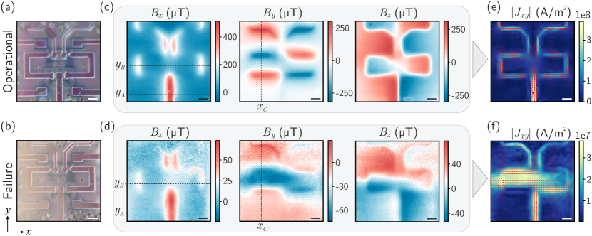
We perform the experiment on two chips: an operational device and a defective one. Investigation of both samples under light-microscopy (Figure 2a,b) reveals no difference. On the contrary, mapping the Oersted fields exposes the failure immediately. With the operating device, Figure 2c shows Oesterd fields clearly reflecting the geometry of the underlying structure. In Figure 2d, we can see that the defective device produces nearly one order of magnitude lower magnetic fields (a maximum amplitude of compared to ). Furthermore, the magnetic field maps and produced by the defective chip show a different unstructured pattern.
To better understand the current distribution producing such Oersted field patterns, we reconstruct the lateral current density . We follow the procedure described in references roth_using_1989 ; meltzer_direct_2017 and use the components of the magnetic field and to numerically invert the Biot-Savart law (eq. (1)), resulting in the current density shown in Figure 2e-f (see Supplementary Information). The maps show the lateral current density amplitude integrated over the vertical axis . In the operating device (Figure 2e), the current paths follow the shape of the visible structure in Figure 2a. A closer look at the central part of the map reveals a weak current contribution with wide lateral spreading, indicating that additional currents flow underneath. Moreover, the flow appears significantly weaker in some parts of the circuit, like at the sharp corners. In the defective device (Figure 2f), several current sources produce fields of similar intensity and observing alone is insufficient to comprehend the anomalies in the current path.
To further understand these observations, we investigate the different layer contributions to locate the flow within the device and seek the third dimension of the current density, .
III Localisation of currents inside a multi-layered device
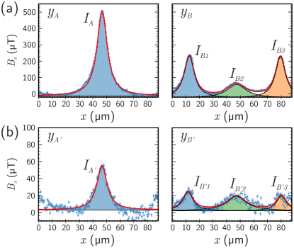
To resolve the signal in the vertical direction , we investigate different linecuts along in the magnetic field map (Figure 3a,b). We fit the linecuts with the Biot-Savart model (Equation (1)), using the infinite wire approximation (Equation (2)),
| (2) |
where is the lateral current amplitude, represents the observation position on the -plane, the position of the current source on the -plane, is the distance between the current source and the observation position on the vertical axis and is a constant offset.
The fitting procedure reveals a contribution from two layers: the first one at away from the layer of NV centres and the second one at (see Supplementary Information). In the operating (failure) case, we identify a current of amplitude () in the main lead dividing into currents of amplitude () and () in two further leads (Figure 3a,b). When comparing the results from the defective device to the operating one, most loss appears on the outer layer (at ), presenting one order of magnitude lower current amplitude. In contrast, the deeper layer (at ) presents a smaller loss. Finally, the analysis of other line profiles reveals another current contribution at present in the operating and defective devices, in both cases with no apparent anomaly (see Supplementary Information). From these observations, we conclude that failure happens in the layer at and then affects the outer layer by propagation.
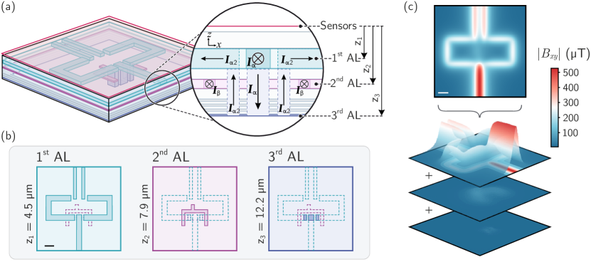
Overall, the simple model with infinite wire approximation already shows excellent agreement with the experimental data. In order to verify the consistency of the procedure, we now perform a simulation of Oersted fields produced by a multi-layered chip. The simulation reproduces the layering of the chip, made of a SiGe technology described in bock_sige_2015 , and some of the apparent geometric features for guidance only.
The total thickness of the simulated structure is and combines twelve stacked layers (Figure 4a). As depicted in Figure 4b, two layers across the structure are electrically active and labelled as active layer (AL) and through-silicon vias (TSV) connect the AL to the bottom layer of the structure. We investigate magnetic fields generated by this structure, resulting in patterns at the position of the sensors shown in Figure 4c. Similarly to the experimental observations (Figure 2), the contribution from the AL is clearly defined and unambiguously related to the shape of the structure. The contribution from the AL shows a pronounced lateral spreading, and the signal arising from two distinct wires starts to blur out. Finally, the contribution from the vertical current is weak due to both the observation position and the presence of counter-propagating flows which average out magnetic field contributions (see Supplementary Information). Still, a current propagating vertically has a nonzero contribution in in contrast to its contribution in . Therefore, currents propagating in the direction can be sensed by NV centres contrary to systems such as SQUIDs (see Supplementary Information).
Lastly, to precisely study the flow in the three-dimensional structure and observe vertical currents, we infer information about the third component of the current density, .
IV Three dimensional current density mapping
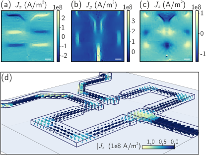
The current-carrying wires have a non-negligible thickness of a few hundred nanometres, leading to a possible contribution of the current’s component. In order to precisely evaluate the total current density, we now consider a component in eq. (1) (see Supplementary Information). The resulting maps are shown in Figure 5a-c, and as for the current density images in Figure 2, they show an integrated signal over the vertical axis . Using the fitting algorithm employed in Figure 3 over the entire map allows us to post-select the signal from the outer layer only. Finally, by applying the current reconstruction procedure on the resulting magnetic maps, we map the three-dimensional current density flow in the outer leads (Figure 5d).
We can see in Figure 5c,d a non-negligible current flow in the -direction at the edges and the corners of the leads, which covers the gaps observed in Figure 2. This information is crucial for evaluating current crowding at corners in interconnect structures, which plays an essential role in nucleating voids and hence failure of ICs pierce_electromigration_1997 ; singh_three-dimensional_2010 ; ceric_electromigration_2011 . Substantially, having access to the full-vector information of the current density helps quantify and understand current flow through different stacks in layered materials. For instance, in the outer layer, we can observe a prominent contribution at the edge of the main branch. As for the simulation (Figure 4), this contribution is the result of counter-propagating currents. Current in the main lead flows down to a deeper layer where it splits into two paths and goes back to the outer layer. As the component does not carry information about and shows a specific pattern with the presence of counter-propagating fields (see Supplementary Information), one can develop an algorithm using with pattern recognition techniques bishop_pattern_2006 to identify the contribution from each current sources.
Resolving currents from different sources across the structure also depends on the spatial resolution of the imaging technique. NV centres offer the closest sensor-sample proximity known so far, but the geometry and capping layers of the microelectronics itself limit the spatial resolution to a few micrometres. In order to non-destructively resolve each layer with high resolution, the solution is to interpolate the current distribution at the source plane using additional layout information. The structure’s layout information can be obtained using circuit designs when available or using ptychographic X-ray laminography techniques holler_three-dimensional_2019 when the sample is unknown. Thus, combining NV-based imaging to X-ray imaging toraille_combined_2020 will allow us to infer the complete information of nanoscale three-dimensional current-carrying structures with no prior information.
V Conclusions
Using NV centres in diamond, we have demonstrated prior-free imaging of three-dimensional current density in a multi-layered integrated circuit. First, we have compared the current flow in an operational chip and a defective one. Exploiting the NV centre high dynamic range, we observed one order of magnitude lower current amplitude in the defective chip. To further understand the failure, we have shown how to localise currents originating in different leads and, in particular, decorrelating the signal originating from several stacked layers. Finally, we have presented imaging of the three vectorial components of the current density. Although the out-of-plane component of the current density is generally neglected in current density imaging techniques, we revealed a significant out-of-plane contribution of close to sharp edges.
Beyond its use for the semiconductor industry to meet the ever-increasing failure analysis needs wolf_3d_2016 , charge transport in electronic systems is fundamental to many phenomena and processes in science and technology falk_nearfield_2009 ; xu_microscale_2005 ; weber_ohms_2012 ; lundstrom_applied_2003 . Therefore, unravelling three-dimensional electronic signals using our method will leverage progress in many areas. For instance, it will serve neuroimaging to overcome the limits of conventional current density imaging techniques and help to reveal new features eroglu_reconstruction_2021 .
Besides, it will help understanding fundamental open problems in three-dimensional correlated systems yang_quantum_2014 ; wang_classification_2014 .
Over the past decade, many efforts have been deployed to both improve the sensing capabilities of the NV centres edmonds_characterisation_2021 ; tetienne_spin_2018 ; mccloskey_enhanced_2020 ; schloss_simultaneous_2018 ; ziem_quantitativeMRI_2019 and to develop techniques to explore new regimes zopes_high-resolution_2017 ; zopes_reconstruction_free_2019 ; mizuno_simultaneous_2020 ; bian_nanoscale_2021 . These combined advances led to remarkable achievements such as revealing electric fields associated with surface band bending in diamond broadway_spatial_2018 and probing Johnson noise in metals kolkowitz_probing_2015 . The advancements can be further used to lower the current sensitivity to the nA range with sub-micron spatial resolution. Such a capability would allow resolving even weak current density fluctuations and possibly provide new insight into the local conductance of materials in condensed matter physics. Ultimately, the NV-based microscope is an up-and-coming platform to characterise different aspects of semiconductors casola_probing_2018 .
VI Methods
VI.1 Diamond substrate
The diamond plates are fabricated by a combination of electron-beam lithography and reactive ion plasma etching. Prior to fabrication, NV centres are created by implantation of nitrogen with an energy of and an implantation dose of into a 100-oriented CVD diamond (quantum grade, Element Six). After implantation, the diamond is annealed at for 2 hours at a pressure of . The plates used here are thick and in size. First, a tiny drop of UV-curable glue is placed on the IC sample. The diamond with the array of plates is then brought in close proximity to the sample with the NV layer facing towards the sample. An individual plate is then broken out of the array using a sharp tungsten tip mounted to a micromanipulator. By optical inspection, it is confirmed that the plate has not flipped during this step which means that the NV layer is facing the IC. The UV-curable glue is hardened after the plate has been fine-positioned to its final location.
VI.2 Experimental set-up and measurement
The NV imaging set-up is a custom-built wide-field fluorescence microscope similar to the one used in ziem_quantitativeMRI_2019 ; steinert_high_2010 . The microscope consists of an air objective (Olympus MPLAPON , NA = 0.95), a long-pass filter (Omega), a tube lens and a Cascade II:512 CCD camera (512 512 pixels, Photometrics), resulting in an effective pixel width of about on the object side.
Experimental realisation of continuous-wave ODMR data was achieved by exciting NV centres with a laser (Coherent) gated with an acousto-optical modulator (Crystal Technology) and coupled into the optical path with a dichroic mirror (Semrock). Simultaneously, microwave radiations were generated using an MW source (RhodeSchwarz SMBV100A) and amplified (100S1G4, Amplifier Research) before being sent to a -thick copper wire. The resulting MW power sent to the wire was approximately 30 dBm. For all the measurements reported in the main text, the total continuous-wave laser power at the back aperture of the objective was about . The camera settings were set to pixel-binning and the field of view (FOV) was defined to .
The IC chip was wire bonded to a printed circuit board (PCB) with -thick gold wires. The PCB was electrically connected to a power supply (RhodeSchwarz Hameg) generating of supply voltage needed to run the chip and an additional bias signal was used to vary the total current sent to the main circuit.
All measurements were performed in an ambient environment at room temperature, under a bias magnetic field generated using a permanent magnet thermally stabilised at a temperature of .
VII Acknowledgements
We gratefully acknowledge T. Rendler for valuable discussions and technical assistance. We acknowledge the support of the European Union’s Horizon 2020 research and innovation programme under the Marie Skłodowska-Curie grant agreement N "765267" (QuSCo) and N "820394" (ASTERIQS). This work was supported by the European research council via SMeL, DFG via GRK 2642.
References
- (1) M. M. Waldrop, “The chips are down for Moore’s law,” Nature News, vol. 530, p. 144, Feb. 2016.
- (2) Q. Xu, B. Schmidt, S. Pradhan, and M. Lipson, “Micrometre-scale silicon electro-optic modulator,” Nature, vol. 435, pp. 325–327, May 2005.
- (3) H. Iwai and S. Ohmi, “Silicon integrated circuit technology from past to future,” Microelectronics Reliability, vol. 42, pp. 465–491, Apr. 2002.
- (4) M. Riordan and L. Hoddeson, “Crystal Fire: The Invention, Development and Impact of the Transistor, Adapted from Chapter 1 of Crystal Fire: The Birth of the Information Age, by Michael Riordan and Lillian Hoddeson, published in 1997 by W. W. Norton & Company.,” IEEE Solid-State Circuits Newsletter, vol. 12, no. 2, pp. 24–29, 2007.
- (5) T. Berners-Lee, R. Cailliau, A. Luotonen, H. F. Nielsen, and A. Secret, “The World-Wide Web,” Communications of the ACM, vol. 37, pp. 76–82, Aug. 1994.
- (6) I. Skog and P. Handel, “In-Car Positioning and Navigation Technologies—A Survey,” IEEE Transactions on Intelligent Transportation Systems, vol. 10, pp. 4–21, Mar. 2009.
- (7) N. Bhatia and M. El-Chami, “Leadless pacemakers: a contemporary review,” Journal of Geriatric Cardiology : JGC, vol. 15, pp. 249–253, Apr. 2018.
- (8) G. E. Moore, “Cramming more components onto integrated circuits, Reprinted from Electronics, volume 38, number 8, April 19, 1965, pp.114 ff.,” IEEE Solid-State Circuits Society Newsletter, vol. 11, pp. 33–35, Sept. 2006.
- (9) D. Mamaluy and X. Gao, “The fundamental downscaling limit of field effect transistors,” Applied Physics Letters, vol. 106, p. 193503, May 2015.
- (10) P. Bhargava, T. Kim, C. V. Poulton, J. Notaros, A. Yaacobi, E. Timurdogan, C. Baiocco, N. Fahrenkopf, S. Kruger, T. Ngai, Y. Timalsina, M. R. Watts, and V. Stojanovic, “Fully Integrated Coherent LiDAR in 3D-Integrated Silicon Photonics/65nm CMOS,” in 2019 Symposium on VLSI Circuits, (Kyoto, Japan), pp. C262–C263, IEEE, June 2019.
- (11) J. Gambetta, “IBM Quantum State of the Union.” IBM Quantum Summit (2021).
- (12) S. Salahuddin, K. Ni, and S. Datta, “The era of hyper-scaling in electronics,” Nature Electronics, vol. 1, pp. 442–450, Aug. 2018.
- (13) E. P. DeBenedictis, M. Badaroglu, A. Chen, T. M. Conte, and P. Gargini, “Sustaining Moore’s law with 3D chips,” Computer, vol. 50, no. 8, pp. 69–73, 2017.
- (14) A. Lancaster and M. Keswani, “Integrated circuit packaging review with an emphasis on 3D packaging,” Integration, vol. 60, pp. 204–212, Jan. 2018.
- (15) H. Wang, D. Forte, M. M. Tehranipoor, and Q. Shi, “Probing Attacks on Integrated Circuits: Challenges and Research Opportunities,” IEEE Design & Test, vol. 34, pp. 63–71, Oct. 2017.
- (16) L. E. Fong, J. R. Holzer, K. K. McBride, E. A. Lima, F. Baudenbacher, and M. Radparvar, “High-resolution room-temperature sample scanning superconducting quantum interference device microscope configurable for geological and biomagnetic applications,” Review of Scientific Instruments, vol. 76, p. 053703, May 2005.
- (17) B. D. Schrag and G. Xiao, “Submicron electrical current density imaging of embedded microstructures,” Applied Physics Letters, vol. 82, pp. 3272–3274, May 2003.
- (18) A. Herrera-May, L. Aguilera-Cortés, P. García-Ramírez, and E. Manjarrez, “Resonant Magnetic Field Sensors Based On MEMS Technology,” Sensors, vol. 9, pp. 7785–7813, Sept. 2009.
- (19) F. Jelezko and J. Wrachtrup, “Single defect centres in diamond: A review,” physica status solidi (a), vol. 203, pp. 3207–3225, Oct. 2006.
- (20) M. W. Doherty, N. B. Manson, P. Delaney, F. Jelezko, J. Wrachtrup, and L. C. Hollenberg, “The nitrogen-vacancy colour centre in diamond,” Physics Reports, vol. 528, pp. 1–45, July 2013.
- (21) G. Balasubramanian, I. Y. Chan, R. Kolesov, M. Al-Hmoud, J. Tisler, C. Shin, C. Kim, A. Wojcik, P. R. Hemmer, A. Krueger, T. Hanke, A. Leitenstorfer, R. Bratschitsch, F. Jelezko, and J. Wrachtrup, “Nanoscale imaging magnetometry with diamond spins under ambient conditions,” Nature, vol. 455, pp. 648–651, Oct. 2008.
- (22) S. Steinert, F. Dolde, P. Neumann, A. Aird, B. Naydenov, G. Balasubramanian, F. Jelezko, and J. Wrachtrup, “High sensitivity magnetic imaging using an array of spins in diamond,” Review of Scientific Instruments, vol. 81, p. 043705, Apr. 2010.
- (23) A. Batalov, V. Jacques, F. Kaiser, P. Siyushev, P. Neumann, L. J. Rogers, R. L. McMurtrie, N. B. Manson, F. Jelezko, and J. Wrachtrup, “Low Temperature Studies of the Excited-State Structure of Negatively Charged Nitrogen-Vacancy Color Centers in Diamond,” Physical Review Letters, vol. 102, p. 195506, May 2009.
- (24) S. Steinert, F. Ziem, L. T. Hall, A. Zappe, M. Schweikert, N. Götz, A. Aird, G. Balasubramanian, L. Hollenberg, and J. Wrachtrup, “Magnetic spin imaging under ambient conditions with sub-cellular resolution,” Nature Communications, vol. 4, p. 1607, June 2013.
- (25) J. Happacher, D. Broadway, P. Reiser, A. Jiménez, M. A. Tschudin, L. Thiel, D. Rohner, M. l. G. Puigibert, B. Shields, J. R. Maze, V. Jacques, and P. Maletinsky, “Low temperature photo-physics of single NV centers in diamond,” arXiv:2105.08075 [cond-mat, physics:quant-ph], May 2021.
- (26) G.-Q. Liu, X. Feng, N. Wang, Q. Li, and R.-B. Liu, “Coherent quantum control of nitrogen-vacancy center spins near 1000 kelvin,” Nature Communications, vol. 10, p. 1344, Dec. 2019.
- (27) M. Lesik, T. Plisson, L. Toraille, J. Renaud, F. Occelli, M. Schmidt, O. Salord, A. Delobbe, T. Debuisschert, L. Rondin, P. Loubeyre, and J.-F. Roch, “Magnetic measurements on micrometer-sized samples under high pressure using designed NV centers,” Science, vol. 366, pp. 1359–1362, Dec. 2019.
- (28) T. Wolf, P. Neumann, K. Nakamura, H. Sumiya, T. Ohshima, J. Isoya, and J. Wrachtrup, “Subpicotesla Diamond Magnetometry,” Physical Review X, vol. 5, p. 041001, Oct. 2015.
- (29) C. Zhang, F. Shagieva, M. Widmann, M. Kübler, V. Vorobyov, P. Kapitanova, E. Nenasheva, R. Corkill, O. Rhrle, K. Nakamura, H. Sumiya, S. Onoda, J. Isoya, and J. Wrachtrup, “Diamond Magnetometry and Gradiometry Towards Subpicotesla dc Field Measurement,” Physical Review Applied, vol. 15, p. 064075, June 2021.
- (30) K. Chang, A. Eichler, J. Rhensius, L. Lorenzelli, and C. L. Degen, “Nanoscale Imaging of Current Density with a Single-Spin Magnetometer,” Nano Letters, vol. 17, pp. 2367–2373, Apr. 2017.
- (31) A. Nowodzinski, M. Chipaux, L. Toraille, V. Jacques, J.-F. Roch, and T. Debuisschert, “Nitrogen-Vacancy centers in diamond for current imaging at the redistributive layer level of Integrated Circuits,” Microelectronics Reliability, vol. 55, pp. 1549–1553, Aug. 2015.
- (32) M. J. Turner, N. Langellier, R. Bainbridge, D. Walters, S. Meesala, T. M. Babinec, P. Kehayias, A. Yacoby, E. Hu, M. Lončar, R. L. Walsworth, and E. V. Levine, “Magnetic Field Fingerprinting of Integrated-Circuit Activity with a Quantum Diamond Microscope,” Physical Review Applied, vol. 14, p. 014097, July 2020.
- (33) B. J. Roth, N. G. Sepulveda, and J. P. Wikswo, “Using a magnetometer to image a two-dimensional current distribution,” Journal of Applied Physics, vol. 65, pp. 361–372, Jan. 1989.
- (34) A. Y. Meltzer, E. Levin, and E. Zeldov, “Direct Reconstruction of Two-Dimensional Currents in Thin Films from Magnetic-Field Measurements,” Physical Review Applied, vol. 8, p. 064030, Dec. 2017.
- (35) J. Böck, K. Aufinger, S. Boguth, C. Dahl, H. Knapp, W. Liebl, D. Manger, T. F. Meister, A. Pribil, J. Wursthorn, R. Lachner, B. Heinemann, H. Rücker, A. Fox, R. Barth, G. Fischer, S. Marschmeyer, D. Schmidt, A. Trusch, and C. Wipf, “SiGe HBT and BiCMOS process integration optimization within the DOTSEVEN project,” in 2015 IEEE Bipolar/BiCMOS Circuits and Technology Meeting - BCTM, pp. 121–124, Oct. 2015.
- (36) D. Pierce and P. Brusius, “Electromigration: A review,” Microelectronics Reliability, vol. 37, pp. 1053–1072, July 1997.
- (37) N. Singh, A. F. Bower, and S. Shankar, “A three-dimensional model of electromigration and stress induced void nucleation in interconnect structures,” Modelling and Simulation in Materials Science and Engineering, vol. 18, p. 065006, Sept. 2010.
- (38) H. Ceric and S. Selberherr, “Electromigration in submicron interconnect features of integrated circuits,” Materials Science and Engineering: R: Reports, vol. 71, pp. 53–86, Feb. 2011.
- (39) C. M. Bishop, “Pattern Recognition and Machine Learning,” in Pattern Recognition and Machine Learning, Springer New York, 2006.
- (40) M. Holler, M. Odstrcil, M. Guizar-Sicairos, M. Lebugle, E. Müller, S. Finizio, G. Tinti, C. David, J. Zusman, W. Unglaub, O. Bunk, J. Raabe, A. F. J. Levi, and G. Aeppli, “Three-dimensional imaging of integrated circuits with macro- to nanoscale zoom,” Nature Electronics, vol. 2, pp. 464–470, Oct. 2019.
- (41) L. Toraille, A. Hilberer, T. Plisson, M. Lesik, M. Chipaux, B. Vindolet, C. Pépin, F. Occelli, M. Schmidt, T. Debuisschert, N. Guignot, J.-P. Itié, P. Loubeyre, and J.-F. Roch, “Combined synchrotron x-ray diffraction and NV diamond magnetic microscopy measurements at high pressure,” New Journal of Physics, vol. 22, p. 103063, Oct. 2020.
- (42) I. D. Wolf, “3-D Technology: Failure Analysis Challenges,” Electronic Device Failure Analysis, vol. 18, no. 4, p. 6, 2016.
- (43) A. L. Falk, F. H. L. Koppens, C. L. Yu, K. Kang, N. de Leon Snapp, A. V. Akimov, M.-H. Jo, M. D. Lukin, and H. Park, “Near-field electrical detection of optical plasmons and single-plasmon sources,” Nature Physics, vol. 5, pp. 475–479, July 2009.
- (44) B. Weber, S. Mahapatra, H. Ryu, S. Lee, A. Fuhrer, T. C. G. Reusch, D. L. Thompson, W. C. T. Lee, G. Klimeck, L. C. L. Hollenberg, and M. Y. Simmons, “Ohm’s Law Survives to the Atomic Scale,” Science, vol. 335, pp. 64–67, Jan. 2012.
- (45) M. Lundstrom, “APPLIED PHYSICS: Enhanced: Moore’s Law Forever?,” Science, vol. 299, pp. 210–211, Jan. 2003.
- (46) H. H. Eroğlu, O. Puonti, C. Göksu, F. Gregersen, H. R. Siebner, L. G. Hanson, and A. Thielscher, “On the reconstruction of magnetic resonance current density images of the human brain: Pitfalls and perspectives,” NeuroImage, vol. 243, p. 118517, Nov. 2021.
- (47) B.-J. Yang, E.-G. Moon, H. Isobe, and N. Nagaosa, “Quantum criticality of topological phase transitions in three-dimensional interacting electronic systems,” Nature Physics, vol. 10, pp. 774–778, Oct. 2014.
- (48) C. Wang, A. C. Potter, and T. Senthil, “Classification of Interacting Electronic Topological Insulators in Three Dimensions,” Science, vol. 343, pp. 629–631, Feb. 2014.
- (49) A. M. Edmonds, C. A. Hart, M. J. Turner, P.-O. Colard, J. M. Schloss, K. S. Olsson, R. Trubko, M. L. Markham, A. Rathmill, B. Horne-Smith, W. Lew, A. Manickam, S. Bruce, P. G. Kaup, J. C. Russo, M. J. DiMario, J. T. South, J. T. Hansen, D. J. Twitchen, and R. L. Walsworth, “Characterisation of CVD diamond with high concentrations of nitrogen for magnetic-field sensing applications,” Materials for Quantum Technology, vol. 1, p. 025001, June 2021.
- (50) J.-P. Tetienne, R. W. de Gille, D. A. Broadway, T. Teraji, S. E. Lillie, J. M. McCoey, N. Dontschuk, L. T. Hall, A. Stacey, D. A. Simpson, and L. C. L. Hollenberg, “Spin properties of dense near-surface ensembles of nitrogen-vacancy centers in diamond,” Physical Review B, vol. 97, p. 085402, Feb. 2018.
- (51) D. J. McCloskey, N. Dontschuk, D. A. Broadway, A. Nadarajah, A. Stacey, J.-P. Tetienne, L. C. L. Hollenberg, S. Prawer, and D. A. Simpson, “Enhanced Widefield Quantum Sensing with Nitrogen-Vacancy Ensembles Using Diamond Nanopillar Arrays,” ACS Applied Materials & Interfaces, vol. 12, pp. 13421–13427, Mar. 2020.
- (52) J. M. Schloss, J. F. Barry, M. J. Turner, and R. L. Walsworth, “Simultaneous Broadband Vector Magnetometry Using Solid-State Spins,” Physical Review Applied, vol. 10, p. 034044, Sept. 2018.
- (53) F. Ziem, M. Garsi, H. Fedder, and J. Wrachtrup, “Quantitative nanoscale MRI with a wide field of view,” Scientific Reports, vol. 9, p. 12166, Dec. 2019.
- (54) J. Zopes, K. Sasaki, K. S. Cujia, J. M. Boss, K. Chang, T. F. Segawa, K. M. Itoh, and C. L. Degen, “High-Resolution Quantum Sensing with Shaped Control Pulses,” Physical Review Letters, vol. 119, p. 260501, Dec. 2017.
- (55) J. Zopes and C. Degen, “Reconstruction-Free Quantum Sensing of Arbitrary Waveforms,” Physical Review Applied, vol. 12, p. 054028, Nov. 2019.
- (56) K. Mizuno, H. Ishiwata, Y. Masuyama, T. Iwasaki, and M. Hatano, “Simultaneous wide-field imaging of phase and magnitude of AC magnetic signal using diamond quantum magnetometry,” Scientific Reports, vol. 10, p. 11611, July 2020.
- (57) K. Bian, W. Zheng, X. Zeng, X. Chen, R. Stöhr, A. Denisenko, S. Yang, J. Wrachtrup, and Y. Jiang, “Nanoscale electric-field imaging based on a quantum sensor and its charge-state control under ambient condition,” Nature Communications, vol. 12, p. 2457, Apr. 2021.
- (58) D. A. Broadway, N. Dontschuk, A. Tsai, S. E. Lillie, C. T.-K. Lew, J. C. McCallum, B. C. Johnson, M. W. Doherty, A. Stacey, L. C. L. Hollenberg, and J.-P. Tetienne, “Spatial mapping of band bending in semiconductor devices using in situ quantum sensors,” Nature Electronics, vol. 1, pp. 502–507, Sept. 2018.
- (59) S. Kolkowitz, A. Safira, A. A. High, R. C. Devlin, S. Choi, Q. P. Unterreithmeier, D. Patterson, A. S. Zibrov, V. E. Manucharyan, H. Park, and M. D. Lukin, “Probing Johnson noise and ballistic transport in normal metals with a single-spin qubit,” Science, vol. 347, pp. 1129–1132, Mar. 2015.
- (60) F. Casola, T. van der Sar, and A. Yacoby, “Probing condensed matter physics with magnetometry based on nitrogen-vacancy centres in diamond,” Nature Reviews Materials, vol. 3, p. 17088, Jan. 2018.