Lightly-strained germanium quantum wells with hole mobility exceeding one million
Abstract
We demonstrate that a lightly-strained germanium channel () in an undoped Ge/Si0.1Ge0.9 heterostructure field effect transistor supports a 2D hole gas with mobility in excess of cm2/Vs and percolation density less than cm-2. This low disorder 2D hole system shows tunable fractional quantum Hall effect at low density and low magnetic field. The low-disorder and small effective mass () defines lightly-strained germanium as a basis to tune the strength of the spin-orbit coupling for fast and coherent quantum hardware.
Quantum confined holes in germanium are emerging as a compelling platform for quantum information processing because of several favorable properties.Scappucci et al. (2021) The light hole effective mass ( at zero density)Lodari et al. (2019) and the absence of valley degeneracyTerrazos et al. (2021); Del Vecchio et al. (2020) give rise to large orbital splittings in quantum dots.Hendrickx et al. (2018) The intrinsic sizable and tunable spin-orbit coupling (SOC)Froning et al. (2021a); Bosco et al. (2021) enables all-electrical fast qubit driving.Watzinger et al. (2018); Hendrickx et al. (2020); Froning et al. (2021b); Wang et al. (2022) Furthermore, the capability to host superconducting pairing correlationsMizokuchi et al. (2018); Hendrickx et al. (2019); Aggarwal et al. (2021) is promising for the co-integration of spin-qubits with superconductors in hybrid architectures for spin–spin long-distance entanglement and quantum information transfer between different qubit types.Choi et al. (2000); Hu et al. (2012); Leijnse and Flensberg (2012, 2013); Hassler et al. (2015); Hoffman et al. (2016); Rančić et al. (2019)
Planar Ge/SiGe heterostructures are promising for scaling up to large quantum processors due to their compatibility with advanced semiconductor manufacturing.Pillarisetty (2011) The low-disorder in planar Ge quantum wellsLodari et al. (2021) enabled the demonstration of a four-qubit quantum processor based on hole spins in a two-by-two array of quantum dots.Hendrickx et al. (2021) These heterostructures featured a Si0.2Ge0.8 strain-relaxed buffer (SRB), resulting in quantum wells with compressive strain .Sammak et al. (2019) Alternatively, higher strained Ge () on Si0.25Ge0.75 SRBs enabled singlet-triplet spin qubits.Jirovec et al. (2021) Lightly-strained Ge/SiGe heterostructures are unexplored and could offer potentially larger SOC because of the reduced energy splitting between heavy-holes (HH) and light holes (LH),Moriya et al. (2014) which is meV for Ge/Si0.1Ge0.9 compared to meV for Ge/Si0.2Ge0.8, respectively.Del Vecchio et al. (2020); Terrazos et al. (2021) As such, lightly-strained Ge is interesting for exploring faster spin-qubit driving and for topological devices. In this letter we demonstrate that lightly-strained Ge quantum wells in undoped Ge/Si0.1Ge0.9 support a two-dimensional hole gas (2DHG) with low disorder at low density, a prerequisite for further exploration of lightly-strained Ge quantum devices.
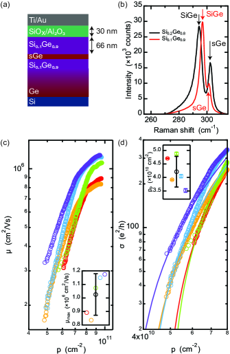
We grow the Ge/SiGe heterostructure by reduced-pressure chemical vapor deposition on a Si(001) wafer and then we fabricate Hall-bar shaped heterostructure field effect transistors (H-FETs) with the same process as in Refs. Sammak et al. (2019); Lodari et al. (2019, 2021). Here, a 16 nm strained Ge (sGe) quantum well (QW) is positioned between two strain-relaxed layers of Si0.1Ge0.9, at a depth of 66 nm [schematics in Fig. 1(a)].111The chemical composition of the layers is measured by secondary ion mass spectroscopy Applying a negative DC bias to the accumulation gate induces a 2DHG at the Ge/Si0.1Ge0.9 interface. The density in the 2DHG is increased above the percolation density by making more negative. We use standard four-probe low-frequency lock-in techniques for mobility-density and magnetotransport characterization at K and mK, with excitation source-drain bias of 1 mV and 100 , respectively. We do not measure gate to drain current leakage over the range of applied . Figure 1(b) shows the Raman spectra measured with a 633 nm red laser to determine the strain in the Ge QW. Comparing Ge/Si0.1Ge0.9 (red) to a control Ge/Si0.2Ge0.8 (black), we observe the Raman peak from the Ge-Ge vibration mode (sGe) in the QW appearing at a lower Raman shift. Conversely, the Raman peak from the SiGe layer is appearing at a higher Raman shift. These observations are consistent with the QW in Ge/Si0.1Ge0.9 being less strained due to a Ge-richer SiGe SRB.Pezzoli et al. (2008) From the position of the Raman shift ( cm-1), we estimate a light compressive strain of for the QW in Ge/Si0.1Ge0.9. This is significantly lower than in Refs. Sammak et al. (2019); Jirovec et al. (2021).
Moving on to electrical characterisation, we operate the H-FET as following. We turn on the device at V and sweep to larger negative voltages ( V) to saturate the traps at the semiconductor/dielectric interface via charge tunneling from the quantum well, similarly to what observed in shallow Ge/Si0.2Ge0.8 H-FETs.Sammak et al. (2019) At these large gate voltages, the density reaches saturation () when the Fermi level crosses the surface quantum well at the Si0.1SiGe0.9/dielectric interface,Su et al. (2017) thereby screening the electric field at the sGe QW.Laroche et al. (2016) Fig. 1(c) shows the mobility as a function of Hall density from five H-FETs fabricated on a cm2 coupon from the center of the 100 mm wafer and measured at K. The mobility increases steeply with due to the increasing screening of scattering from remote charged impurities.Monroe (1993); Gold (2010); Laroche et al. (2016) At higher density ( cm-2), short range scattering from impurities within and/or in proximity of the quantum well becomes the mobility-limiting scattering mechanism.Laroche et al. (2016) We observe a maximum mobility in the range of cm2/Vs for in the range of cm-2 over the five investigated H-FETs. The inset in Fig. 1(c) shows a box plot of across the devices, with an average value of cm2/Vs (black), setting a benchmark for holes in buried channel transistors. Crucially, such high mobility is measured at very low density below cm-2, a significant improvement compared to previous studies in Ge/SiGe.Sammak et al. (2019); Lodari et al. (2021)
Beyond , is a key metric for characterizing the disorder potential landscape at low density, the regime relevant for quantum dot qubits. Figure 1(d) shows the conductivity (circles) as a function of density for all the investigated devices and their fit to percolation theory (lines) , where the exponent is fixed for 2D systems.Tracy et al. (2009) ranges from to cm-2. Figure 1(d) inset shows a box plot of the percolation density across the devices with an average value of cm-2 (black). We take these values as an upper bound for , since we observed smaller values of [ cm-2 at mK] if the range of applied gate voltage is restricted to small voltages above the turn-on threshold.
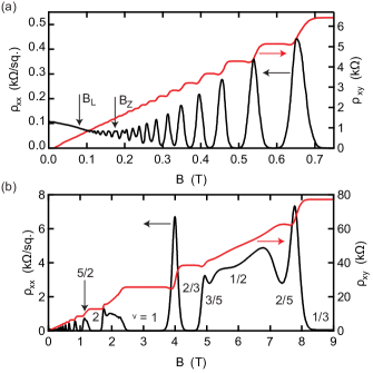
Since Ge/S0.1Ge0.9 is characterized by such low level of disorder, we further explored the quantum transport proprieties of the 2DHG at mK. Figure 2(a) shows the longitudinal resistivity (black) and transverse Hall resistivity (red) as a function of perpendicular magnetic field up to T and at a Hall density of cm-2 and cm2/Vs. We observe clear Shubnikov–de Haas (SdH) resistivity oscillations above mT. The onset for resolving the spin-degeneracy by Zeeman splitting is T and minima reach zero already at T. We do not observe beatings in the SdH oscillations associated with increased Rashba spin-splitting. We speculate that such beatings are more likely to be visible at higher densities, that require the quantum well to be closer to the dielectric interface.Lodari et al. (2019)
Fig. 3(b) shows the SdH oscillations at higher magnetic fields: strong minima are developed for filling factors with integer and fractional values. Clear plateaus are visible in for and , where correspondingly vanishes. Such high quality fractional quantum Hall effect (FQHE) has previously only been reported holes in modulation-doped systems at higher carrier density and, hence, at larger magnetic fields.Shi et al. (2015); Mironov et al. (2016); Berkutov et al. (2019) Here, in undoped heterostructure, we use the top-gate to follow the evolution of FQHE states down to low density, providing avenues for studying the underlying physics.
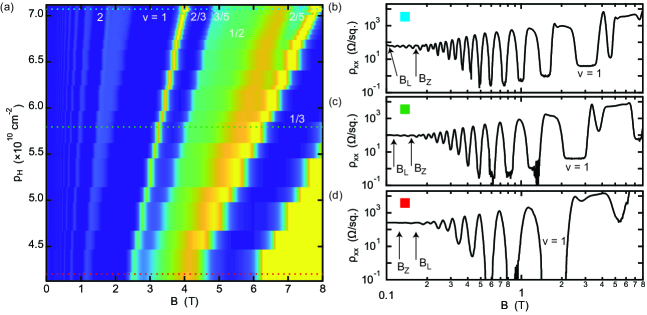
The color map in Fig. 3(a), measured at mK, shows (normalized to the value at zero magnetic field) as a function of magnetic field and Hall density in the range of cm-2. Yellow and blue regions in the color map correspond to peaks and dips in the normalized , highlighting the density-dependent evolution of integer and fractional filling factors. All filling factors fan out towards higher magnetic field and density, and fractional filling factors are well resolved across the full investigated range of density and magnetic field. Three line cuts from the color map are shown in Fig. 3(b–d), at decreasing density (blue), (green), and cm-2 (red), respectively. We observe that the minima associated with fractional become shallower as the density is decreased, possibly because of increased level broadening by unscreened disorder and because of weaker Coulomb interactions and correlation effects.Mironov et al. (2016); Berkutov et al. (2019) We also observe the distance between the onset of Shubnikov-de Haas oscillations () and Zeeman splitting () reducing from Fig. 3(b) to Fig. 3(c). In Fig. 3(d), and have crossed, meaning that at cm-2 the Zeeman gap is larger than the cyclotron gap and therefore the spin susceptibility ,Lu et al. (2017) where is the effective mass and the effective g-factor out of plane. Indeed, from thermal activation measurement (Supplementary Material) we estimate and at a density of cm-2, corresponding to a spin susceptibility of 1. We note that similar values of and were reported in Ge/Si0.2Ge0.8Lodari et al. (2019); Hendrickx et al. (2018) albeit at much higher density, pointing to higher HH-LH intermixing in the lightly strained quantum wells at lower density, as expected from theory.Terrazos et al. (2021)
In conclusion, we demonstrated a lightly-strained Ge/SiGe heterostrucure supporting a 2DHG with mobility in excess of one million and low percolation density (less than cm-2). Such low disorder enables measurement of FQHE at tunable low density and low magnetic fields. To mitigate the effect of traps at the interface and to suppress tunneling from the quantum well to the surface, we speculate that lightly-strained Ge channels could be positioned deeper compared to more strained channelsSu et al. (2017); Lodari et al. (2021) because of the smaller band offset ( meV Ge/Si0.2Ge0.9 vs. meV in Ge/Si0.2Ge0.8). Further measurements in quantum dots, where confinement increases the HH-LH mixing, will help to elucidate the effect of reduced strain on the spin-orbit coupling in the system. The demonstration that holes can be defined in QWs with varying strain provides avenues to explore the opportunities in the germanium quantum information route.
I Supplemental Material
Supplemental material is provided with measurements of the effective -factor and effective mass.
II Acknowledgment
G.S. and M.V. acknowledge support through a projectruimte grant associated with the Netherlands Organization of Scientific Research (NWO). This work is partially funded by the ARC Centre of Excellence for Future Low Energy Electronics Technologies (N0. CE170100039).
III Data availability
Data sets supporting the findings of this study are available at doi.org/10.4121/17306906.v1.
References
- Scappucci et al. (2021) G. Scappucci, C. Kloeffel, F. A. Zwanenburg, D. Loss, M. Myronov, J.-J. Zhang, S. De Franceschi, G. Katsaros, and M. Veldhorst, Nature Reviews Materials 6, 926 (2021).
- Lodari et al. (2019) M. Lodari, A. Tosato, D. Sabbagh, M. A. Schubert, G. Capellini, A. Sammak, M. Veldhorst, and G. Scappucci, Physical Review B 100, 041304 (2019).
- Terrazos et al. (2021) L. A. Terrazos, E. Marcellina, Z. Wang, S. N. Coppersmith, M. Friesen, A. R. Hamilton, X. Hu, B. Koiller, A. L. Saraiva, D. Culcer, and R. B. Capaz, Phys. Rev. B 103, 125201 (2021).
- Del Vecchio et al. (2020) P. Del Vecchio, M. Lodari, A. Sammak, G. Scappucci, and O. Moutanabbir, Phys. Rev. B 102, 115304 (2020).
- Hendrickx et al. (2018) N. W. Hendrickx, D. P. Franke, A. Sammak, M. Kouwenhoven, D. Sabbagh, L. Yeoh, R. Li, M. L. Tagliaferri, M. Virgilio, G. Capellini, G. Scappucci, and M. Veldhorst, Nature Communications 9, 1 (2018), arXiv:1801.08869 .
- Froning et al. (2021a) F. N. M. Froning, M. J. Rančić, B. Hetényi, S. Bosco, M. K. Rehmann, A. Li, E. P. A. M. Bakkers, F. A. Zwanenburg, D. Loss, D. M. Zumbühl, and F. R. Braakman, Physical Review Research 3, 013081 (2021a).
- Bosco et al. (2021) S. Bosco, M. Benito, C. Adelsberger, and D. Loss, Physical Review B 104, 115425 (2021).
- Watzinger et al. (2018) H. Watzinger, J. Kukučka, L. Vukušić, F. Gao, T. Wang, F. Schäffler, J.-J. Zhang, and G. Katsaros, Nature Communications 9, 3902 (2018).
- Hendrickx et al. (2020) N. W. Hendrickx, D. P. Franke, A. Sammak, G. Scappucci, and M. Veldhorst, Nature 577, 487 (2020), arXiv:1904.11443 .
- Froning et al. (2021b) F. N. M. Froning, L. C. Camenzind, O. A. H. van der Molen, A. Li, E. P. A. M. Bakkers, D. M. Zumbühl, and F. R. Braakman, Nature Nanotechnology 16, 308 (2021b).
- Wang et al. (2022) K. Wang, G. Xu, F. Gao, H. Liu, R.-L. Ma, X. Zhang, Z. Wang, G. Cao, T. Wang, J.-J. Zhang, D. Culcer, X. Hu, H.-W. Jiang, H.-O. Li, G.-C. Guo, and G.-P. Guo, Nature Communications 13, 206 (2022), arXiv: 2006.12340.
- Mizokuchi et al. (2018) R. Mizokuchi, R. Maurand, F. Vigneau, M. Myronov, and S. De Franceschi, Nano Letters 18, 4861 (2018).
- Hendrickx et al. (2019) N. W. Hendrickx, M. L. V. Tagliaferri, M. Kouwenhoven, R. Li, D. P. Franke, A. Sammak, A. Brinkman, G. Scappucci, and M. Veldhorst, Phys. Rev. B 99, 075435 (2019).
- Aggarwal et al. (2021) K. Aggarwal, A. Hofmann, D. Jirovec, I. Prieto, A. Sammak, M. Botifoll, S. Martí-Sánchez, M. Veldhorst, J. Arbiol, G. Scappucci, J. Danon, and G. Katsaros, Phys. Rev. Research 3, L022005 (2021).
- Choi et al. (2000) M.-S. Choi, C. Bruder, and D. Loss, Physical Review B 62, 13569 (2000).
- Hu et al. (2012) X. Hu, Y.-x. Liu, and F. Nori, Physical Review B 86, 035314 (2012).
- Leijnse and Flensberg (2012) M. Leijnse and K. Flensberg, Physical Review B 86, 104511 (2012).
- Leijnse and Flensberg (2013) M. Leijnse and K. Flensberg, Physical Review Letters 111, 060501 (2013).
- Hassler et al. (2015) F. Hassler, G. Catelani, and H. Bluhm, Physical Review B 92, 235401 (2015).
- Hoffman et al. (2016) S. Hoffman, C. Schrade, J. Klinovaja, and D. Loss, Physical Review B 94, 045316 (2016).
- Rančić et al. (2019) M. J. Rančić, S. Hoffman, C. Schrade, J. Klinovaja, and D. Loss, Physical Review B 99, 165306 (2019).
- Pillarisetty (2011) R. Pillarisetty, Nature 479, 324 (2011).
- Lodari et al. (2021) M. Lodari, N. W. Hendrickx, W. I. L. Lawrie, T.-K. Hsiao, L. M. K. Vandersypen, A. Sammak, M. Veldhorst, and G. Scappucci, Materials for Quantum Technology 1, 011002 (2021), arXiv:2007.06328 .
- Hendrickx et al. (2021) N. W. Hendrickx, W. I. L. Lawrie, M. Russ, F. van Riggelen, S. L. de Snoo, R. N. Schouten, A. Sammak, G. Scappucci, and M. Veldhorst, Nature 591, 580 (2021).
- Sammak et al. (2019) A. Sammak, D. Sabbagh, N. W. Hendrickx, M. Lodari, B. Paquelet Wuetz, A. Tosato, L. R. Yeoh, M. Bollani, M. Virgilio, M. A. Schubert, P. Zaumseil, G. Capellini, M. Veldhorst, and G. Scappucci, Advanced Functional Materials 29, 1 (2019).
- Jirovec et al. (2021) D. Jirovec, A. Hofmann, A. Ballabio, P. M. Mutter, G. Tavani, M. Botifoll, A. Crippa, J. Kukucka, O. Sagi, F. Martins, J. Saez-Mollejo, I. Prieto, M. Borovkov, J. Arbiol, D. Chrastina, G. Isella, and G. Katsaros, Nature Materials 20, 1106 (2021).
- Moriya et al. (2014) R. Moriya, K. Sawano, Y. Hoshi, S. Masubuchi, Y. Shiraki, A. Wild, C. Neumann, G. Abstreiter, D. Bougeard, T. Koga, and T. Machida, Physical Review Letters 113, 086601 (2014).
- Note (1) The chemical composition of the layers is measured by secondary ion mass spectroscopy.
- Pezzoli et al. (2008) F. Pezzoli, E. Bonera, E. Grilli, M. Guzzi, S. Sanguinetti, D. Chrastina, G. Isella, H. Von Känel, E. Wintersberger, J. Stangl, and G. Bauer, Journal of Applied Physics 103 (2008), 10.1063/1.2913052.
- Su et al. (2017) Y.-H. Su, Y. Chuang, C.-Y. Liu, J.-Y. Li, and T.-M. Lu, Phys. Rev. Materials 1, 044601 (2017).
- Laroche et al. (2016) D. Laroche, S. H. Huang, Y. Chuang, J. Y. Li, C. W. Liu, and T. M. Lu, Applied Physics Letters 108 (2016), 10.1063/1.4953399.
- Monroe (1993) D. Monroe, Journal of Vacuum Science Technology B: Microelectronics and Nanometer Structures 11, 1731 (1993).
- Gold (2010) A. Gold, Journal of Applied Physics 108 (2010), 10.1063/1.3482058.
- Tracy et al. (2009) L. A. Tracy, E. H. Hwang, K. Eng, G. A. Ten Eyck, E. P. Nordberg, K. Childs, M. S. Carroll, M. P. Lilly, and S. Das Sarma, Physical Review B - Condensed Matter and Materials Physics 79, 1 (2009).
- Shi et al. (2015) Q. Shi, M. A. Zudov, C. Morrison, and M. Myronov, Phys. Rev. B 91, 241303 (2015).
- Mironov et al. (2016) O. A. Mironov, N. d’Ambrumenil, A. Dobbie, D. R. Leadley, A. V. Suslov, and E. Green, Phys. Rev. Lett. 116, 176802 (2016).
- Berkutov et al. (2019) I. B. Berkutov, V. V. Andrievskii, Y. A. Kolesnichenko, and O. A. Mironov, Low Temperature Physics 45, 1202 (2019).
- Lu et al. (2017) T. M. Lu, L. A. Tracy, D. Laroche, S.-H. Huang, Y. Chuang, Y.-H. Su, J.-Y. Li, and C. W. Liu, Scientific Reports 7, 2468 (2017).