Ultrafast Multi-Shot Ablation and Defect Generation in Monolayer Transition Metal Dichalcogenides
Abstract
Transition metal dichalcogenides are known to possess large optical nonlinearities and driving these materials at high intensities is desirable for many applications. Understanding their optical responses under repetitive intense excitation is essential to improve the performance limit of these strong-field devices and to achieve efficient laser patterning. Here, we report the incubation study of monolayer \chMoS2 and \chWS2 induced by , pulses in air to examine how their ablation threshold scales with the number of admitted laser pulses. Both materials were shown to outperform graphene and most bulk materials; specifically, \chMoS2 is as resistant to radiation degradation as the best of the bulk thin films with a record fast saturation. Our modeling provides convincing evidence that the small reduction in threshold and fast saturation of \chMoS2 originates in its excellent bonding integrity against radiation-induced softening. Sub-ablation damages, in the forms of vacancies, strain, lattice disorder, and nano-voids, were revealed by transmission electron microscopy, photoluminescence, Raman, and second harmonic generation studies, which were attributed to the observed incubation in 2D materials. For the first time, a sub-ablation damage threshold is identified for monolayer \chMoS2 to be 78% of single-shot ablation threshold, below which \chMoS2 remains intact for many laser pulses. Our results firmly establish \chMoS2 as a robust material for strong-field devices and for high-throughput laser patterning.
Understanding the optical responses of two-dimensional (2D) materials under strong excitation is important. For example, semiconductor transition metal dichalcogenides (TMDs) have demonstrated strong optical nonlinearities such as second harmonic generation (SHG),[1, 2] high harmonic generation,[3] saturable absorption,[4, 5] and giant two-photon and three-photon absorption.[6, 7, 8] These properties make TMDs an excellent candidate for attosecond photonics, mode locking, optical limiting, and multi-photon detectors. For such applications, performance is limited by the optical damage of 2D materials so understanding the laser-induced damage in any forms of defects under repetitive excitation is critical to improve their performance metrics. Additionally, ultrafast lasers have been demonstrated to selectively remove 2D materials for specific sizes and geometries.[9, 10] Compared to electron-beam and photolithography which have high costs, complexity, and degraded device performance due to unwanted dopants, contaminates, and polymer residues,[11] ultrafast laser ablation is a promising technique to pattern 2D materials that is in situ, resist-free, and maskless. For this application, knowledge of multi-shot ablation is essential to select optimal laser parameters to deterministically remove material. As the onset of ablation and damage are governed by similar physical principles, determining the ablation threshold fluences of 2D materials as a function of the number of pulses admitting on the same spot of the substrate is important.
Such a phenomenon, commonly referred to as incubation, is well known in pulsed laser-induced ablation and damage of bulk materials.[12] Starting from the single-shot ablation threshold , the threshold fluence decreases monotonically with until it approximately saturates at . For , varies in a small range of fluence, defined as . If the fluence is below , ablation does not occur for any number of pulses, at least theoretically. The ratio is a measure of the degree of incubation: the larger the , the less pronounced the incubation and the more resistant the material is to radiation damage. We note that the incubation study of graphene was previously reported by Wetzel et al. but their study was purely experimental without any discussion or understanding.[13] On the other hand, femtosecond multi-shot degradation of monolayer \chMoS2 was reported by Paradisanos et al.[14] They observed softening of the Raman and modes at two fluences (25% and 40% of ), which they attributed to a decrease of the Mo-S bond density. Incubation in terms of and their signatures beyond Raman scattering for monolayer TMDs has not been reported.
In this work, the multi-shot ablation threshold for monolayer \chMoS2 and \chWS2 is studied and described based on a phenomenological model for the first time. We also carried out transmission electron microscopy (TEM), and second harmonic generation (SHG), photoluminescence (PL), and Raman spectroscopies to reveal morphological and optical property changes in \chMoS2 in the sub-ablation damage regime to provide insight into defect formation. The saturation threshold is found to be about 75% of the single-shot ablation threshold and coincides with the damage threshold as measured by second harmonic generation. This provides direct evidence that incubation begins with laser-induced defects in 2D materials, including vacancies and lattice distortion.
Monolayer \chMoS2 films and \chWS2 flakes were grown by chemical vapor deposition on c-cut sapphire (\chAl2O3) and transferred to a borosilicate glass and \chAl2O3 substrate, respectively.[15] A Coherent RegA 9000 producing pulses at a central wavelength of is used to conduct all ablation experiments. The repetition rate was kept constant at where a mechanical shutter was used to select a single or multiple pulses from the pulse train. The laser pulse energy was controlled using a continuous neutral density filter wheel or a half-wave plate with a polarizer, where a calibrated, fast photodiode was used to record individual pulse energies . The pulses were focused on to the \chMoS2 film by a 10, 0.26 NA objective which also allowed for in situ imaging of the experiment. The \chMoS2 sample was mounted on an Aerotech ANT three-axis motorized translation stage for precise positioning control.
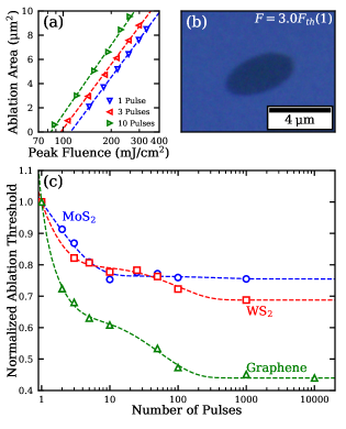
The ablation threshold was determined by measuring the ablated hole area as a function of the incident peak fluence where the linear extrapolation of the hole area versus yields the threshold fluence at zero area.[16] This area method is illustrated in Fig. 1 for \chMoS2 on a glass substrate and , 3, and 10 pulses. For fluences above , the ablation produces deterministic holes with a well-defined shape, as illustrated in Fig. 1. The effective laser spot radius was as measured by both a CCD camera and the fits in Fig. 1. Figure 1 shows the normalized of \chMoS2 and \chWS2 for selective up to 1000 pulses. As a comparison, the incubation for graphene from Ref. 13 is also shown. For reference, the values of and for each of these materials are summarized in Table 1. For \chMoS2, decreases monotonically from to 10 before saturating at . For \chWS2 and graphene, quickly reduces for the first three pulses and then experiences an inflection, before leveling off at 1000 pulses. The values for \chMoS2 and \chWS2 were found to be larger than the majority of bulk materials.[12, 17, 18] Only \chHfO2 (, , ) and \chTa2O5 (, , ) films were found to have comparable values to \chMoS2 and \chWS2, respectively.[19, 18] Among all these materials, \chMoS2 has the fastest saturation.
To model the data, we generalize the phenomenological model introduced by Sun et al. to 2D materials, which was formulated in terms of the change in absorption and critical bulk energy density.[12] We assume the absorption and the critical surface energy density change over successive pulses according to
| (1) | ||||
where is the initial absorption, is its maximal change (typically positive), is the initial critical surface energy density needed for single-shot ablation, is its maximal change (typically negative), and the coefficients and are rate constants. Importantly, is the internal fluence inside the 2D materials where represents the intensity enhancement factor due to the interference effect of the supporting substrate, which are and 0.53 for borosilicate glass and \chAl2O3, respectively.[10] Using the internal fluence allows the determination of substrate independent coefficients. According to this model, the threshold fluence is reached when the energy density deposited by the pulse equals the critical energy density modified by the preceding pulses:
| (2) |
By combining Eqs. (1) and (2), the multi-shot threshold satisfies the following transcendental equation
| (3) |
where is the intrinsic single-shot ablation threshold and is the intrinsic multi-shot ablation threshold at saturation. From Eq. (3), can be expressed as a simple analytical function of the maximal fractional change in critical energy and absorption according to
| (4) |
To obtain a large value, Eq. (4) indicates and should be as close to zero as possible. Equation (3) is applied to fit experimental data in Fig. 1 to extract the fitting parameters , , and . is then calculated from Eq. (4). The dashed curves in Fig. 1 are the theoretical fits where all the fitting parameters are shown in Table 1. This model provides insight into the incubation behavior of these 2D materials. Though they have similar values, is negligible for \chMoS2, yielding the largest and the smallest with a single decay trend in its incubation. For \chWS2 and graphene, the initial fast decay of is due to a strong saturation of with the number of pulses (i.e. large ), followed by a slow decay due to a weak saturation of (i.e. small ), leading to a larger . The transition between these two decays manifests the inflection in Fig. 1.
| Materials |
|
|
|
|||||||||
|---|---|---|---|---|---|---|---|---|---|---|---|---|
| \chMoS2 | 111 | 0.75 | 0.31 | -0.013 | 6.3 | 0.052 | ||||||
| \chWS2 | 161 | 0.69 | 0.25 | -0.14 | 13 | 0.16 | ||||||
| Graphene | 156 | 0.44 | 0.55 | -0.32 | 15 | 0.35 |
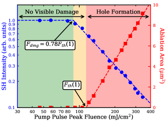
To gain information on the structural changes induced by the laser exposure, we performed a correlated study of the ablation area and SHG, since SHG is known to be sensitive to changes in crystal structure. In this experiment, the \chMoS2 sample is exposed to a single intense pump pulse, followed by a train of weaker pulses to probe the resultant structural modification using static SHG. The result is shown in Fig. 2 for various pump fluences below and above . For fluences above where holes are created deterministically, the SH signal decreases with increasing fluence, which can be understood in terms of the reduced spatial overlap of the probe pulse with the edges of the hole. For pump fluences below 89, the SH intensity remained the same as that of pristine \chMoS2, indicating the material is intact. Between them where no visible hole was seen, the SH signal is still below the pristine value, indicating that the film is permanently damaged. Accordingly, we define the sub-ablation damage threshold fluence as the minimal fluence causing permanent damage to the film. At this limit, the damage most likely consists of localized vacancies and lattice disorder. Importantly, comparing Figs. 1 and 2 yields . This finding clearly proves that such laser-induced defects represent the beginning stages of incubation for ablation. As long as the pulse fluence is below , monolayer \chMoS2 will not be ablated for any number of pulses . Similarly, for , each pulse will generate sub-ablation damage, accumulatively creating a deterministic hole at its zero-area limit by the pulse.
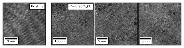
To visualize such sub-ablation damage, a \chMoS2 film was transferred to a holey carbon film grid for high resolution transmission electron microscopy (HR-TEM). The left image in Fig. 3 shows a HR-TEM image of pristine \chMoS2 where the dark spots represent the sulfur atoms and the bright spots are the molybdenum atoms. The images on the right show \chMoS2 exposed to a single pulse at where clusters of atoms ranging up to a few nanometers across are removed without destroying the overall integrity of the film. Figure 3 reveals that such sub-ablation damage is stochastic in nature where voids appear sporadic with random sizes and shapes within the exposed area. This is in sharp contrast to the deterministic ablated holes seen in the area method (Fig. 1). The nano-voids in Fig. 3 show a decrease of roughly 5% in atomic density, as determined by ImageJ analysis, which translates to a 10% reduction in SH intensity. Figure 2, however, indicates a 20% reduction in SH intensity, implying the presence of other defects in addition to the nano-voids. Again, this supports the existence of vacancies and lattice disorder as suggested in Fig. 2, which are beyond the resolution of our TEM.
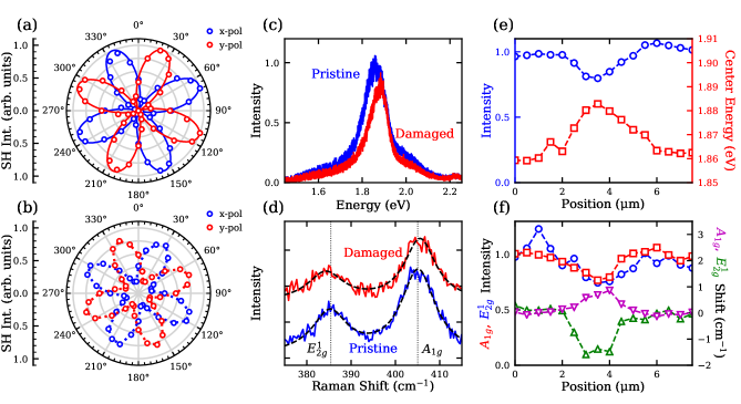
To reveal more optical signatures of these defects, we performed various optical spectroscopies on pristine \chMoS2 and \chMoS2 exposed to a single pulse at . Figure 4 shows the SH polar profile for pristine \chMoS2 by rotating the incident polarization while recording the SH signal at x- and y-polarizations. The data follows the theoretical curve (solid line) for this method, indicating excellent crystallinity.[1] The polar profile at the center of the damaged region is shown in Fig. 4. As the damaged region is significantly smaller than the probe pulse spot size, the SH signal is dominated by the surrounding pristine \chMoS2 where a 4-fold symmetry is still clearly resolved. Compared to Fig. 4, however, the depolarization (reduced contrast) is evident where the maximal SH intensity reduces by 20% and the minimum never drops completely to zero. A more pronounced depolarization can be seen for \chMoS2 exposed to where more of the SH signal is from the edge of the hole (see the supporting information). In addition to SHG, Figs. 4-4 show the PL and Raman spectra recorded at the center of the damaged spot. As a reference, pristine spectra are also shown in blue. The line profile of the PL peak intensity and center energy scanned across the damaged spot is presented in Fig. 4, showing an intensity reduction of 25% and a blue shift of 0.02 eV after exposure. Similar results were also recorded for the Raman line scan as shown in Fig. 4, where the intensity of both the and peaks are reduced by 25% in the damage region. Additionally, the mode experiences a maximal red shift of while the peak shows a maximal blue shift of .
For single pulse exposure at , the reduction of the Mo-S bonds is estimated below 5% from Fig. 3, indicating other defects play a significant role in the observed 20%-25% drop in SH, PL, and Raman intensities. The presence of vacancies and disorder breaks the lattice translational symmetry, which compromises the constructive and destructive interference among SH dipoles across the sample. This will reduce the maximal SH signal and increase the minimal SH signal in the polar plot, consistent with the observed de-polarization effect in Fig. 4. In addition, dangling bonds associated with these vacancies are known to introduce mid-gap states. Several types of vacancies associated with S and Mo atoms are shown to generate mid-gap states with energies ranging from 0.02 to 1.72 eV within the band gap, which can provide non-radiative decay pathways.[20, 21, 22, 23] These states have been invoked to strongly quench the PL intensity and cause a blue shift similar to that observed here.[24, 25, 26, 27, 28] The blue shift in the PL peak can also be attributed to the adsorption of oxygen on the \chMoS2 monolayer given the ambient conditions of the experiment.[27] Moreover, occupation of these mid-gap states by the preceding pulses could increase the light absorption of successive laser pulses during incubation, leading to a reduction in threshold fluence.[21] Additionally, the lateral strain introduced locally by these vacancies and lattice disorder can cause the Raman intensities to decrease.[29, 30] The blue shift in the and red shift in the peaks could be explained by a combination of p-doping from the presence of Mo-O bonds[31, 32] and strain introduced by these defects.[27, 29]
In summary, we show that \chMoS2 and \chWS2 have weak incubation effects when excited by , pulses in air. A modified phenomenological model based on the change in surface energy density and absorption was applied to describe the incubation behavior of \chMoS2, \chWS2, and graphene with good agreement. According to this model, \chMoS2 has negligible laser-induced bond softening, yielding its weakest incubation () and fastest saturation (). For a \chMoS2 film exposed to a single pulse at a fluence below , our TEM analysis reveals nano-voids and our optical spectroscopy data strongly support the presence of atomic-scale defects such as vacancies and lattice distortion, which are responsible for the observed reduction and peak energy shift in PL and Raman, as well as reduced contrast in polarized SHG. Moreover, static SH measurements identify the threshold fluence to generate such defects to be for \chMoS2, which coincides with and provides direct evidence that laser-induced defects set the beginning stages of incubation for ablation of \chMoS2. For fluences below , \chMoS2 remains intact for an infinite number of pulses. For fluences slightly above , incubation starts with laser generated atomic defects. Successive pulse exposure leads to nano-voids with random sizes and shapes, which grow in size with subsequent pulses, until a deterministic ablation hole with a theoretical zero area is reached. For fluences between and , nano-voids could form during the first shot, requiring fewer number of pulses to reach the onset of ablation. The above conclusion is expected to apply qualitatively to \chWS2. To understand quantitatively the difference of incubation between these two materials, a microscopic model involving multiple kinetic rate equations is needed.[33] While such a model better describes the physics of incubation, its implementation is challenging since many properties associated with these defects in 2D materials such as their energy levels and lifetimes are not known in literature or are speculative at best. The fast saturation and weak incubation establish \chMoS2 as an attractive material for high-throughput laser processing and strong field devices.
Acknowledgements.
This research was supported by the Ministry of Science and Technology (MOST) of Taiwan (Grant No’s. 109-2112-M-009-020-MY3, 109-2124-M-009-003-MY3, MOST-110-2119-M-A49-001-MBK) and the Center for Emergent Functional Matter Science (CEFMS) of NYCU supported by the Ministry of Education of Taiwan.Author Declarations
The authors have no conflicts to disclose.
Data Availability Statement
The data that supports the findings in this study are available within the article and its supporting information.
References
- Mannebach et al. [2014] E. M. Mannebach, K.-A. N. Duerloo, L. A. Pellouchoud, M.-J. Sher, S. Nah, Y.-H. Kuo, Y. Yu, A. F. Marshall, L. Cao, E. J. Reed, and A. M. Lindenberg, “Ultrafast Electronic and Structural Response of Monolayer MoS2 under Intense Photoexcitation Conditions,” ACS Nano 8, 10734–10742 (2014).
- Kumar et al. [2013] N. Kumar, S. Najmaei, Q. Cui, F. Ceballos, P. M. Ajayan, J. Lou, and H. Zhao, “Second harmonic microscopy of monolayer MoS2,” Physical Review B 87, 161403 (2013).
- Liu et al. [2017] H. Liu, Y. Li, Y. S. You, S. Ghimire, T. F. Heinz, and D. A. Reis, “High-harmonic generation from an atomically thin semiconductor,” Nature Physics 13, 262–265 (2017).
- Wang et al. [2013a] K. Wang, J. Wang, J. Fan, M. Lotya, A. O’Neill, D. Fox, Y. Feng, X. Zhang, B. Jiang, Q. Zhao, H. Zhang, J. N. Coleman, L. Zhang, and W. J. Blau, “Ultrafast Saturable Absorption of Two-Dimensional MoS2 Nanosheets,” ACS Nano 7, 9260–9267 (2013a).
- Nie et al. [2018] Z. Nie, C. Trovatello, E. A. A. Pogna, S. Dal Conte, P. B. Miranda, E. Kelleher, C. Zhu, I. C. E. Turcu, Y. Xu, K. Liu, G. Cerullo, and F. Wang, “Broadband nonlinear optical response of monolayer MoSe2 under ultrafast excitation,” Applied Physics Letters 112, 31108 (2018).
- Li et al. [2015] Y. Li, N. Dong, S. Zhang, X. Zhang, Y. Feng, K. Wang, L. Zhang, and J. Wang, “Giant two-photon absorption in monolayer MoS2,” Laser & Photonics Reviews 9, 427–434 (2015).
- Zhang et al. [2015] S. Zhang, N. Dong, N. McEvoy, M. O’Brien, S. Winters, N. C. Berner, C. Yim, Y. Li, X. Zhang, Z. Chen, L. Zhang, G. S. Duesberg, and J. Wang, “Direct Observation of Degenerate Two-Photon Absorption and Its Saturation in WS2 and MoS2 Monolayer and Few-Layer Films,” ACS Nano 9, 7142–7150 (2015).
- Zhou and Ji [2017] F. Zhou and W. Ji, “Giant Three-Photon Absorption in Monolayer MoS2 and Its Application in Near-Infrared Photodetection,” Laser & Photonics Reviews 11, 1700021 (2017).
- Park, Yoo, and Grigoropoulos [2012] J. B. Park, J.-H. Yoo, and C. P. Grigoropoulos, “Multi-scale graphene patterns on arbitrary substrates via laser-assisted transfer-printing process,” Applied Physics Letters 101, 43110 (2012).
- Solomon et al. [2021] J. M. Solomon, S. I. Ahmad, A. Dave, L.-S. Lu, F. HadavandMirzaee, S.-C. Lin, S.-H. Chen, C.-W. Luo, W.-H. Chang, and T.-H. Her, “Ultrafast Laser Ablation, Intrinsic Threshold, and Nanopatterning of Monolayer Molybdenum Disulfide,” arXiv e-prints , arXiv:2111.01352 (2021), arXiv:2111.01352 [physics.optics] .
- Kollipara, Li, and Zheng [2020] P. S. Kollipara, J. Li, and Y. Zheng, “Optical Patterning of Two-Dimensional Materials,” Research 2020, 6581250 (2020).
- Sun, Lenzner, and Rudolph [2015] Z. Sun, M. Lenzner, and W. Rudolph, “Generic incubation law for laser damage and ablation thresholds,” Journal of Applied Physics 117, 73102 (2015).
- Wetzel et al. [2013] B. Wetzel, C. Xie, P.-A. Lacourt, J. M. Dudley, and F. Courvoisier, “Femtosecond laser fabrication of micro and nano-disks in single layer graphene using vortex Bessel beams,” Applied Physics Letters 103, 241111 (2013).
- Paradisanos et al. [2014] I. Paradisanos, E. Kymakis, C. Fotakis, G. Kioseoglou, and E. Stratakis, “Intense femtosecond photoexcitation of bulk and monolayer MoS2,” Applied Physics Letters 105, 41108 (2014).
- Hsu et al. [2019] W.-F. Hsu, L.-S. Lu, P.-C. Kuo, J.-H. Chen, W.-C. Chueh, H. Yeh, H.-L. Kao, J.-S. Chen, and W.-H. Chang, “Monolayer MoS2 Enabled Single-Crystalline Growth of AlN on Si(100) Using Low-Temperature Helicon Sputtering,” ACS Applied Nano Materials 2, 1964–1969 (2019).
- Liu [1982] J. M. Liu, “Simple technique for measurements of pulsed Gaussian-beam spot sizes,” Optics Letters 7, 196–198 (1982).
- Rosenfeld et al. [1999] A. Rosenfeld, M. Lorenz, R. Stoian, and D. Ashkenasi, “Ultrashort-laser-pulse damage threshold of transparent materials and the role of incubation,” Applied Physics A 69, S373–S376 (1999).
- Mero et al. [2005] M. Mero, B. R. Clapp, J. C. Jasapara, W. G. Rudolph, D. Ristau, K. Starke, J. Krüger, S. Martin, and W. Kautek, “On the damage behavior of dielectric films when illuminated with multiple femtosecond laser pulses,” Optical Engineering 44, 1–7 (2005).
- Nguyen et al. [2008] D. N. Nguyen, L. Emmert, M. Mero, W. G. Rudolph, D. Patel, E. Krous, and C. S. Menoni, “The effect of annealing on the subpicosecond breakdown behavior of hafnia films,” in Proc.SPIE, Vol. 7132 (2008).
- Hong et al. [2015] J. Hong, Z. Hu, M. Probert, K. Li, D. Lv, X. Yang, L. Gu, N. Mao, Q. Feng, L. Xie, J. Zhang, D. Wu, Z. Zhang, C. Jin, W. Ji, X. Zhang, J. Yuan, and Z. Zhang, “Exploring atomic defects in molybdenum disulphide monolayers,” Nature Communications 6, 6293 (2015).
- Khan et al. [2017] M. A. Khan, M. Erementchouk, J. Hendrickson, and M. N. Leuenberger, “Electronic and optical properties of vacancy defects in single-layer transition metal dichalcogenides,” Physical Review B 95, 245435 (2017).
- Bahmani et al. [2020] M. Bahmani, M. Faghihnasiri, M. Lorke, A.-B. Kuc, and T. Frauenheim, “Electronic Properties of Defective MoS2 Monolayers Subject to Mechanical Deformations: A First-Principles Approach,” physica status solidi (b) 257, 1900541 (2020).
- Liu, Stradins, and Wei [2016] Y. Liu, P. Stradins, and S.-H. Wei, “Air Passivation of Chalcogen Vacancies in Two-Dimensional Semiconductors,” Angewandte Chemie International Edition 55, 965–968 (2016).
- Ma et al. [2013] Q. Ma, P. M. Odenthal, J. Mann, D. Le, C. S. Wang, Y. Zhu, T. Chen, D. Sun, K. Yamaguchi, T. Tran, M. Wurch, J. L. McKinley, J. Wyrick, K. Magnone, T. F. Heinz, T. S. Rahman, R. Kawakami, and L. Bartels, “Controlled argon beam-induced desulfurization of monolayer molybdenum disulfide,” Journal of Physics: Condensed Matter 25, 252201 (2013).
- Förster et al. [2017] A. Förster, S. Gemming, G. Seifert, and D. Tománek, “Chemical and Electronic Repair Mechanism of Defects in MoS2 Monolayers,” ACS Nano 11, 9989–9996 (2017).
- Sivaram et al. [2019] S. V. Sivaram, A. T. Hanbicki, M. R. Rosenberger, G. G. Jernigan, H.-J. Chuang, K. M. McCreary, and B. T. Jonker, “Spatially Selective Enhancement of Photoluminescence in MoS2 by Exciton-Mediated Adsorption and Defect Passivation,” ACS Applied Materials & Interfaces 11, 16147–16155 (2019).
- Oh et al. [2016] H. M. Oh, G. H. Han, H. Kim, J. J. Bae, M. S. Jeong, and Y. H. Lee, “Photochemical Reaction in Monolayer MoS2 via Correlated Photoluminescence, Raman Spectroscopy, and Atomic Force Microscopy,” ACS Nano 10, 5230–5236 (2016).
- Lu et al. [2015] J. Lu, A. Carvalho, X. K. Chan, H. Liu, B. Liu, E. S. Tok, K. P. Loh, A. H. Castro Neto, and C. H. Sow, “Atomic Healing of Defects in Transition Metal Dichalcogenides,” Nano Letters 15, 3524–3532 (2015).
- Wang et al. [2013b] Y. Wang, C. Cong, C. Qiu, and T. Yu, “Raman Spectroscopy Study of Lattice Vibration and Crystallographic Orientation of Monolayer MoS2 under Uniaxial Strain,” Small 9, 2857–2861 (2013b).
- Kukucska and Koltai [2017] G. Kukucska and J. Koltai, “Theoretical Investigation of Strain and Doping on the Raman Spectra of Monolayer MoS2,” physica status solidi (b) 254, 1700184 (2017).
- Mawlong, Paul, and Giri [2018] L. P. L. Mawlong, K. K. Paul, and P. K. Giri, “Direct Chemical Vapor Deposition Growth of Monolayer MoS2 on TiO2 Nanorods and Evidence for Doping-Induced Strong Photoluminescence Enhancement,” The Journal of Physical Chemistry C 122, 15017–15025 (2018).
- Wu et al. [2013] J. Wu, H. Li, Z. Yin, H. Li, J. Liu, X. Cao, Q. Zhang, and H. Zhang, “Layer Thinning and Etching of Mechanically Exfoliated MoS2 Nanosheets by Thermal Annealing in Air,” Small 9, 3314–3319 (2013).
- Emmert, Mero, and Rudolph [2010] L. A. Emmert, M. Mero, and W. Rudolph, “Modeling the effect of native and laser-induced states on the dielectric breakdown of wide band gap optical materials by multiple subpicosecond laser pulses,” Journal of Applied Physics 108, 43523 (2010).