A Method for Hiding the Increased Non-Volatile Cache Read Latency
Abstract
The increased memory demands of workloads is putting high pressure on Last Level Caches (LLCs). Unfortunately, there is limited opportunity to increase the capacity of LLCs due to the area and power requirements of the underlying SRAM technology. Interestingly, emerging Non-Volatile Memory (NVM) technologies promise a feasible alternative to SRAM for LLCs due to their higher area density. However, NVMs have substantially higher read and write latencies, which offset their area density benefit. Although researchers have proposed methods to tolerate NVM’s increased write latency, little emphasis has been placed on reducing the critical NVM read latency.
To address this problem, this paper proposes Cloak. Cloak exploits data reuse in the LLC at the page level, to hide NVM read latency. Specifically, on certain L1 TLB misses to a page, Cloak transfers LLC-resident data belonging to the page from the LLC NVM array to a set of small SRAM Page Buffers that will service subsequent requests to this page. Further, to enable the high-bandwidth, low-latency transfer of lines of a page to the page buffers, Cloak uses an LLC layout that accelerates the discovery of LLC-resident cache lines from the page. We evaluate Cloak with full-system simulations of a 4-core processor across 14 workloads. We find that, on average, Cloak outperforms an SRAM LLC by 23.8% and an NVM-only LLC by 8.9%—in both cases, with negligible additional area. Further, Cloak’s is 39.9% and 17.5% lower, respectively, than these designs.
I Introduction
The popularity of data intensive workloads, such as HPC applications and web servers, cloud applications and databases, has intensified capacity pressure on Last-Level Caches (LLCs). While much larger LLCs are desired, SRAM technology suffers from high area overhead (exacerbated by the increasing manufacturing cost at leading edge technologies [3, 2]), substantial leakage power, and scalability problems [14].
For these reasons, researchers have examined alternative memory technologies, such as eDRAM and Non-Volatile Memory (NVM). In particular, NVM technologies such as PCM [50] and, especially, STT-RAM [10] are promising candidates to replace SRAM in LLCs. Compared to SRAM, STT-RAM offers higher density and lower leakage power [33]. Unlike eDRAM, NVM is compatible with current logic and SRAM, and can be easily integrated in the same die. Further, compared to eDRAM, NVM offers lower complexity (no refresh, activate, or precharge operations), comparable read access time, and improved power-efficiency due to its ability to power gate without losing state.
However, NVMs have two main shortcomings over SRAM, namely, higher latency for both read and write operations, and a higher dynamic energy consumption per access. Moreover, read and write latencies in NVMs change based on the targeted lifetime endurance (wear-out) of the device. Therefore, replacing an SRAM LLC with an NVM one becomes a trade-off between latency, capacity, reliability and energy consumption. In this paper, we focus on mitigating the long NVM read latency for highly-reliable NVM caches.
Table I compares the characteristics of SRAM and STT-RAM cells. We can see that STT-RAM cells are 4x smaller in area, while their read and write latencies are 10–30x and 25–100x, respectively, higher than SRAM’s. The table does not include the energy and power numbers because the literature provides wide ranges of values, dependent on implementation and manufacturing technology [67, 63, 59, 61, 8]. Specifically, STT-RAM’s leakage power is 0.15–0.48x that of SRAM’s, and its dynamic access energy is 0.8–2.5x higher than SRAM’s for reads and 1.5–15x higher for writes.
| Characteristic | SRAM | STT-RAM |
|---|---|---|
| [7, 56, 31, 54] | [46, 32, 16, 43, 53] | |
| [40, 23, 24, 45, 47] | ||
| Area () | 70-150 | 15-40 |
| Read Latency (ns) | 0.3 | 3 - 10 |
| Write Latency (ns) | 0.3 | 8 - 30 |
Prior work has tried to overcome NVM’s problems of higher latency—primarily write latency—and dynamic power using solutions spanning the device, circuit, and architecture levels. At the device and circuit levels, the write access latency (primarily) can be reduced by sacrificing the retention time and non-volatility of the STT-RAM cells [55, 29, 58, 30]. Also, the transistor size can be adjusted for faster write operation [43], at the cost of higher power, lower density, and lower reliability [33]. Such approaches limit the full potential of NVM caches and do not solve the increased read latency problem. Indeed, degrading NVM characteristics to reduce the write latency introduces the need for periodic refresh, which hurts design complexity and energy consumption, and hinders non-volatility [48, 35]. Additionally, adjusting the NVM cell size to reduce write latency limits NVM capacity and introduces higher error rates [33, 19].
At the architecture level, the most popular solutions to address NVM’s higher latency and dynamic power combine smaller SRAM caches with larger STT-RAM caches in a hybrid cache hierarchy [63, 15, 61, 57]. Unfortunately, these solutions focus mostly on write latency (not the focus of this paper) or use inclusive caches (much less used today). In addition, they use a considerable amount of SRAM memory, plus complex logic to decide which cache lines to swap between SRAM and STT-RAM. As a result, they limit the area savings from NVM and increase the energy consumption.
In terms of access latencies, several proposals mitigate the performance impact of long NVM write latencies [36, 66, 59, 17, 65, 8]. Interestingly, little emphasis has been placed on mitigating the NVM read latency, based on the common assumption that the SRAM and STT-RAM read latencies are similar. However, measurements on fabricated STT-RAM caches and observations by industry vendors show a significant difference in read latency between STT-RAM [67, 64, 63, 46, 32, 16, 43, 24, 45, 47, 40, 23] and SRAM [7, 56, 31]. Specifically, as shown in Table I, FinFET-based 6T SRAM arrays perform read operations with a 300ps latency [31], while the fastest STT-RAMs can only attain 3ns latencies at best [53].
To take advantage of NVM for LLCs, we need a low-cost architectural solution that can tolerate the higher read latency of STT-RAM without sacrificing capacity, reliability, or non-volatility. This paper proposes such an architectural solution, which we call Cloak. Cloak exploits data reuse at the level of pages in the LLC to hide NVM read latency. Specifically, on certain L1 TLB misses to a page, the hardware transfers LLC-resident lines of the page from the LLC NVM array to a set of small SRAM Page Buffers. Such buffers will service future requests to this page. To enable the low latency detection and high-bandwidth transfer of lines of a page to the page buffers, Cloak uses an LLC layout that accelerates the discovery of LLC-resident cache lines from the page. Further, we develop an adaptive replacement policy for the Page Buffers to increase their utilization and achieve better performance and energy consumption.
We evaluate Cloak with full-system simulations of a four-core processor running 14 workloads. On average, Cloak outperforms an SRAM LLC by 23.8% and an NVM-only LLC by 8.9%—in both cases, with negligible additional area. Furthermore, Cloak improves the metric by 39.9% and 17.5%, respectively.
II Background
II-A STT-RAM Limitations and Opportunities
STT-RAM has emerged as a promising candidate to replace SRAM in LLCs [64, 63, 57, 44] because it provides higher density and lower leakage than SRAM. However, the viability of STT-RAM is inhibited by higher read and write access latencies, and by higher dynamic energy than SRAM. This is because STT-RAM requires a high thermal barrier, which in turn increases the switching current of the device and the cell access latency. The high thermal barrier is a consequence of the requirement for a large retention period, typically expected of non-volatile memory cells.
Past research has exploited a trade-off that exists between retention time and write access latency, to design cells whose write access latency is tolerable for practical on-chip integration [29, 55, 58, 30]. Such techniques help lower the device write time to 8–30ns, as shown in Table I. These proposals focus on reducing write latency because read latencies tend to be smaller, namely 3–10ns.
However, one major caveat is that the STT-RAM array latency cannot be pipelined. During the cell access latencies reported in Table I, the array is blocked from servicing other requests. As a result, sustaining high throughput is challenging. In contrast, SRAM array accesses are pipelined, and so data can be moved to/from the cache array every cycle. This leads to both higher throughput and guaranteed maximum latency for accesses.
STT-RAM write latency is constrained by bit-level error guarantees to ensure reliable operation across the lifetime of the chip. In our case, where the STT-RAM LLC is 16MB per slice (Table II), the Bit Error Rate (BER) of the STT-RAM cell needs to be lower than 10-10 to ensure a 99.99999% yield with SECDED ECC. This is based on the assumption that a cache line is fetched from a single STT-RAM macro of 2MB. Based on results from prototype devices[43, 24, 9], STT-RAMs with such error rate guarantees can only achieve a bitcell write latency of 8ns and a read latency of 3.2ns. Furthermore, recent innovations in the quality of magnesium oxide (MgO), which acts as the dielectric material, pave the way for high endurance STT-RAM cells in future designs [60]. As a result, the literature reports that STT-RAM is a competitive alternative to SRAM for L3 caches. It can have an endurance in the order of 1012 to 1013 write cycles [15, 36, 60, 65], especially under normal temperature environments as the one we target [18].
Overall, given the reasonable tradeoffs between STT-RAM write latency and BER, the most pressing problem is to mitigate the impact of the high read latency of large STT-RAM LLCs operating in ambient conditions. This is our focus.
II-B NVM Cache as an SRAM Replacement
Prior work on NVM caches has focused on mitigating the effect of long-latency write operations [36, 66, 59, 17, 65, 8]. The work can be categorized into three groups: methods to reduce, stall or bypass writes to NVM caches, NVM cell optimizations, and hybrid SRAM/NVM caches.
Solutions in the first group identify write contention in the NVM cache that can stall latency-critical reads. Then, they try to take writes off the critical path of subsequent read requests [36, 59, 66, 8]. These techniques assume the same read latency for NVM and SRAM accesses.
Proposals that optimize NVM cells improve NVM cache write performance at the expense of retention time and area [58, 29, 55, 43]. These optimizations are not trivial, given the trade-offs between access latency, area, and retention time of NVMs [64, 10, 19]. In addition, decreasing the retention time of NVMs introduces refreshes, similar to DRAM, which increase energy consumption and complicate the design. Moreover, it limits the capacity of NVMs and introduces higher error rates. Importantly, it does not address the problem of the non-pipelined and high read latency.
Hybrid cache proposals [61, 63, 15, 57] split a cache into an NVM and an SRAM portion, typically by partitioning a cache set into SRAM and NVM ways. These proposals monitor address reuse to place data in the SRAM or NVM parts of the cache.
For energy efficiency, the SRAM and NVM portions of the cache can be powered on/off according to the cache line usage [15]. This approach leads to energy savings at the expense of performance degradation and increased circuit complexity.
For performance, some techniques [61, 63, 57] place the critical data in the SRAM portion of the cache, and the non-critical data in the NVM portion. However, these techniques have several shortcomings. First, they dedicate a large portion of cache capacity to SRAM, therefore reducing the density benefit of NVM and increasing leakage power. The area overhead of the SRAM portion is 25–100%, assuming a 4:1 density between NVM and SRAM [57, 61, 63]. Second, they need large structures of several KBs to accurately monitor cache line activity. Third, they must migrate data between SRAM and NVM, which further increases the number of writes to NVM, the energy consumption, and the area overhead. Fourth, in exclusive and victim LLCs, it is hard to monitor the reuse of individual addresses because LLC hits result in promoting lines to faster levels of the cache hierarchy. As a result, the overhead and complexity of recording data reuse increases. Finally, these techniques do not consider that the non-pipelined nature of NVM accesses introduces high overhead to line migration.
III Motivation
To increase the cache capacity in multi-cores, designers are organizing LLCs as victim caches. We would like to use NVM in the LLC, to enable high capacity caching with high retention time and low error rates. To this end, in this paper, we observe that an L1 TLB miss on a page that was already referenced in the past is a good hint that some LLC-resident cache lines of the page will be reused again soon. Consequently, we would like to identify such TLB refills and bring likely-to-reuse lines from the LLC into a small SRAM structure.
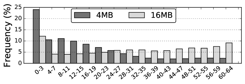
To support this insight, we model a 3-level cache hierarchy with a 16MB L3 and 4KB pages. Figure 1 shows the percentage of L3 hits that originate from pages whose translation was once in the L1 data TLB, was evicted, and then later was re-filled back into the L1 TLB. We observe that such percentage is 94.9%. This data implies that, upon an L1 TLB page re-fill, there should be many requests to this page that hit in the LLC.
Figure 2 shows the number of L3-resident cache lines belonging to a 4KB page that is being re-filled into the L1 TLB for different L3 cache sizes. Such number can be from 0 to 64 lines. We see that, while in most cases we have 0–3 lines, there is a long tail of up to 60-64 resident lines. In addition, as we scale the L3 size from 4MB to 16MB per core, the number of such resident cache lines increases. Therefore, we conclude that the number of requests hitting in the L3 cache and originating from a TLB refilled page likely rises with the L3 size. Cloak builds on these observations to architect a solution that hides the increased read latency of NVM caches and increases overall throughput.
IV Design Overview of CLOAK
IV-A Main Idea
Cloak is a hardware mechanism that takes advantage of certain L1 TLB misses to exploit data re-use in large NVM LLC caches and hide NVM read latency. The NVM LLC cache is augmented with small SRAM buffers, which we call Page Buffers (PB). PBs hold data transferred from the NVM LLC main array. Each PB can hold a copy of LLC-resident cache lines originating from the same page. To trigger the copy of data into a PB, Cloak leverages the L1 data TLBs. When a miss in the L1 TLB occurs for a previously-accessed page, hardware communicates this information to the LLC, which finds all LLC-resident lines from this page and copies them to the PBs.
The lines that were previously accessed from the page have a high chance of being accessed again when the page is re-filled in the L1 TLB—due to temporal locality within a page. Cloak tracks page-level reuse via address translation hardware to infer future references to the NVM cache. To facilitate the retrieval of a page’s cache lines from the LLC, we introduce a new LLC data layout that places the cache lines of a given page in the same physical cache row.
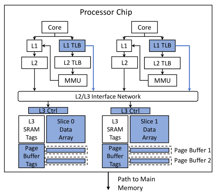
Figure 3 shows the architecture of Cloak, where the new or modified hardware structures are shaded, and the added connections between the L1 TLBs and the L3 Controllers are shown in lighter color. In this section, we describe the overall operation of Cloak to fetch data to the PBs and service memory requests. Subsequently, Section V discusses the architectural details of our design.
IV-B Cloak Overview
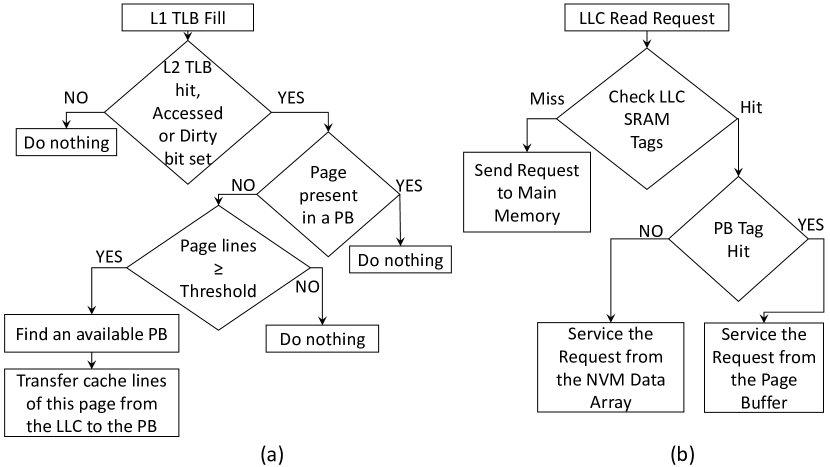
The core operations of Cloak consist of data movement from the NVM data array to the PBs on a TLB signal, and servicing of subsequent requests either from the PBs or the NVM cache array. Figure 4 shows the control flow diagrams of these actions.
IV-B1 TLB triggered Page Buffer transfer
PBs are small SRAM-based cache structures which act as fast access buffers to the NVM LLC. Each PB can hold a subset of the NVM-resident cache lines of a given page. Promoting NVM-resident lines from a page into a PB can hide the read latency of an LLC access, by exploiting intra-page spatial locality [21] and by reducing the number of accesses to the NVM data array.
The promotion of a page’s cache lines to one of the PBs is depicted in Figure 4a. When an L1 TLB miss occurs, the PTE for the page is fetched and Cloak determines whether this page was previously referenced. To identify whether the page was referenced in the past, Cloak checks if the page is in the L2 TLB or, if it is not, if either the Accessed or Dirty bits of its PTE [1] is set. A set Accessed bit indicates that the page was accessed in the past. This bit is set by the hardware when the page is first read or written, and is only reset by the OS to track the frequency of accesses to the page. A set Dirty bit indicates that the page was written, and hence, was referenced before. The Dirty bit is set by the processor the first time that the page is written to, and is only cleared by software.
If Cloak finds that the page was used in the past, it sends a signal to the LLC controller containing the physical address of the request that caused the TLB refill. The LLC controller first determines if a PB already contains lines from this page. If not, Cloak decides whether to transfer the page to a PB and, if so, which PB to use. To decide whether to transfer the page’s lines, Cloak checks the LLC tags to calculate the population of NVM-resident lines of this page. A promotion to a PB occurs only if the population size exceeds a programmable threshold, so that the cost of fetching all the lines to a PB can be amortized across the expected number of PB hits. Then, Cloak selects an available PB to promote the page’s cache lines according to the PB replacement policy (Section V-D).
IV-B2 Servicing requests to the LLC
In Cloak, a hit in the LLC can obtain the data from the NVM cache array or from a PB. The PB contents are kept coherent with the NVM cache. Thus, writes to the LLC (e.g., due to an L2 eviction) also check the PBs and, on a hit, update both the NVM data array and the PB. An acknowledgement, signaling completion of the write request, is sent to the L2 when the request is buffered in the LLC queues. It does not wait until when the request updates the NVM data array and PB.
Figure 4b shows servicing a read request to the LLC. The LLC controller checks the Physical Page Numbers (PPNs) in the PB Tags and in the LLC SRAM tags in parallel, to determine a hit or a miss. If the LLC tag check determines that there is an LLC miss, the request is forwarded to main memory. If the LLC tag check determines an LLC hit and the PB tag check indicates a PB hit, the request is serviced from the PBs otherwise it is serviced from the NVM cache.
In Cloak, an LLC NVM hit can be serviced in parallel with a PB hit to a different address. This does not increase the peak LLC bandwidth because data coming from the PB and from the NVM data array share a single bus to the L2 cache. However, in-flight read accesses to the slow, non-pipelined NVM data array do not block younger reads to the PBs.
V Cloak Implementation
V-A Data Layout
Transferring the lines of a page from the LLC to a PB requires finding all NVM-resident lines of that page. To avoid massive tag lookups and NVM cache read operations, we introduce an alternative data layout for the NVM cache. The proposed layout forces all the lines of a given page to be placed in a single physical row of the LLC. A physical row contains multiple cache sets, each with multiple cache lines, and each physical row may contain lines from multiple pages.
For the Cloak LLC, we assume a physically distributed, logically shared L3 cache that acts as a victim of private L2 caches. While we evaluate a specific design point, the design of Cloak itself does not preclude other potential organizations of the cache hierarchy. The cache is split into equally-sized slices. Each slice has its own controller and can independently service any type of request. We use STT-RAM for the data array and SRAM for the tag array for two reasons. First, the tag array is much smaller than the data array and its relative area overhead is small. Second, the LLC is highly associative, and the tags are accessed before the data array to minimize the dynamic energy of the data array access. Having NVM tags would add significant latency to all accesses.
The LLC tag array supports both conventional accesses (e.g., triggered by L2 misses) and 4KB-aligned page-level data transfer requests triggered by L1 TLB fills. We distinguish the two by referring to the former as Cache Line Requests (CLR) and to the latter as Page Transfer Requests (PTR).
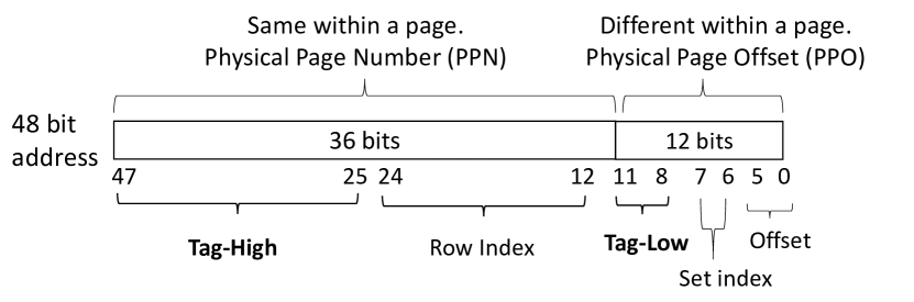
By placing all the lines of a given page in the same LLC physical row, we limit tag searching to only 64 entries for every incoming PTR (assuming 4KB pages and a 64B line size). We alter the LLC cache indexing to support our new data layout for both PTR and CLR accesses. Our addressing scheme is presented in Figure 5. To pick the physical row, we use some bits of the Physical Page Number (PPN) called Row Index. Once the row is selected, we use a subset of the Physical Page Offset (PPO) bits called Set Index to select a set within the physical row. Then, some of the PPN bits (Tag-High) and of the PPO bits (Tag-Low) are used as tag. Finally, the remaining PPO bits are used as block offset (Figure 5).
PTRs and CLRs differ in the tag match logic. Specifically, for tag matching, a PTR access ignores the page offset bits. Hence, it only uses Tag-High bits. In contrast, a CLR access uses both Tag-High and Tag-Low bits for tag matching.
The lines of a page could be split across LLC slices, mapping to the same physical row in each slice. However, in order to simplify the tag hit logic and NVM to PB data movement, we choose to map the entire page in the same LLC slice. Note that our layout does not impose any restrictions on the LLC organization (e.g., line size, associativity, etc.).
Example. To illustrate the proposed layout, we show an example with a single-slice of 32MB size, 16-way set-associative LLC with 64B cache lines and 4KB pages. The LLC has 8192 physical rows, each organized in 4 sets, 16 ways each. Each physical row is 4KB and can be banked if needed. As shown in Figure 5, the physical address (PA) has 48 bits, the 12 least significant ones are the PPO, and bits 0-5 are the line offset.
The cache index bits include the row index bits (bits 24:12), which select the row of the cache, and the set index bits (bits 7:6), which select the cache set within a row. Note that the row index bits (bits 24:12) do not include any PPO bits. Bits 11:8 and 47:25 form the tag, split into Tag-Low and Tag-High parts, respectively. For tag matching, a CLR selects a row and a set using indexing bits 24:12 and 7:6, respectively, and finds a match using the tag bits (bits 47:25 and 11:8). For tag matching, a PTR selects a row using the row index bits (bits 24:12) and finds all matches using the subset of tag bits lying outside the PPO, namely the Tag-High (bits 47:25). Thanks to this data layout, the PTR does not search the entire cache; it only checks the Tag-High (bits 47:25) of the 64 lines in the selected cache row.
The dynamic energy of a CLR tag access is proportional to the 16 lines 27 tag bits comparison (432 bits). The dynamic energy of a PTR tag access is proportional to the 64 lines 23 tag bits comparison (1,472 bits). A PTR tag access consumes 3.4 more energy than a conventional CLR tag access. Triggering PTR tag searches only on TLB re-filled pages lowers the overall energy cost of accessing the PBs.
Our data layout could be extended to optimize for huge pages. However, we find that such a design is not efficient, as huge pages increase the overhead of tag lookup and data movement, while it is unlikely that a large fraction of their lines will be LLC-resident. In Section V-E, we present how we efficiently handle huge pages.
V-B Promotion of Cache Lines to Page Buffers
Cloak populates each PB with LLC-resident cache lines from the same page. The process is as follows. Once a PTR reaches the LLC controller, the hardware checks if any PB already has lines from the accessed page. If not, the hardware checks the LLC tags to find if the LLC holds more than a threshold number of cache lines of the accessed page. If so, the LLC-resident lines of the page are transferred to a PB. The NVM cache is inclusive of the PBs. Hence, the transferred lines are not invalidated from the NVM data array.
Cloak provides hardware to bring cache lines to the PBs. According to Figure 2, the LLC may only contain a few of the lines from a given page. Hence, PBs will be sparsely populated. In order to increase PB utilization, it is preferable to have more and smaller PBs. For this reason, we propose PBs that are smaller than a page. However, given that the size of a physical row is equal to a page, steering the data from a row to a PB is not trivial and requires keeping metadata. To simplify both the metadata and the routing overhead, we propose using PBs of size equal to half a page (2KB), and multiplex the two halves of a page into the same PB.
Example. Figure 6 shows an example that promotes cache lines from page A into a PB. Since we have 4KB pages (and, hence, 4KB physical rows) and use 2KB PBs, we logically partition a physical row into two 2KB regions, and promote the lines of a page into the PB in two steps: first from the leftmost region of the physical row, and then from the rightmost region of the row.
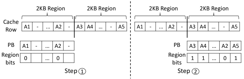
The left side of Figure 6 shows the first step. At the top, we see the the state of the cache row. The leftmost region has lines in its first position (A1) and in the one before last (A2). Hence, we promote these lines into the PB. To simplify the routing, as shown in the figure, the lines are placed in the PB in the same slots that they use in the 2KB region. The PB does not need to store any address tags because any memory access will check the SRAM LLC tags first, to decide whether the corresponding PB line is valid. However, each PB slot has a bit to identify which region the line comes from. This bit is needed to fully identify the line. In the example, since the two lines come from the leftmost region, the bits are 0. In our example, we need 32 such bits, which we call Region bits.
The right side of Figure 6 shows the second step. The top part repeats the cache row state. The rightmost region has lines in its first (A3), second (A4), and last (A5) positions. Hence, we promote these lines into the PB and set the Region bits of the entries to 1.
Note that the two lines in the first position of the two regions wanted to use the same PB slot, and we had to pick a winner. In the example, we picked A3 over A1. To pick a winner, Cloak uses a simple algorithm that tries to guess which of the two lines is more likely to be used in the future. Specifically, Cloak takes the address A that triggered the TLB miss and records whether A belongs to the first or second half of the page. Then, when populating a PB, on a conflict in a PB entry, the line from the same half of the page as A overwrites the line from the different half of the page. This algorithm guesses that, because of spatial locality, the former is more likely to be accessed soon that the latter.
Thanks to LLC’s organization, the operation of promoting the lines from the two regions (and, in another design, from potentially more regions) into a PB does not stall the LLC pipeline more than a single read. Indeed, all the cache lines of a page are on the same physical row, and thus they are promoted to a PB with a single read operation in the NVM data array. The writes into the PB are also pipelined: as the first region is written, the second performs the checks.
V-C Tag Checks
To keep track of the pages and cache lines that are present in the PBs, Cloak has a hardware structure organized as an array called the Page Buffer Tags (PB Tags) (Figure 7). Each entry in the PB Tags corresponds to one PB. An entry has: (a) the PPN of the page whose lines are stored in the PB, (b) a Replacement counter to manage PB replacement, (c) a Residency counter that tracks the number of valid lines in the PB, and (d) the Region bits discussed above.
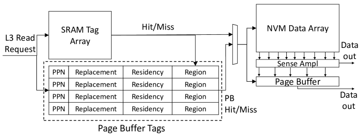
Both PTR and CLR use the PB Tags to determine whether a PB contains data for the page requested. In the case of a PTR, the PB Tags are checked to identify if there is an entry with the PPN of the requested page. In a CLR, the PB Tags are checked to identify if there is an entry with the requested PPN and with the correct bit in the Region field corresponding to the requested line.
The operation of a CLR is as follows. The CLR accesses both the LLC tag array and PB Tags simultaneously (Figure 7). It uses the PPN bits of the PB Tags to identify if a PB contains lines from the page accessed. It uses the LLC tag array to identify whether and where the requested line resides in the LLC physical row. If the address of the line is not found in the LLC tag array, an LLC miss is declared.
However, if the LLC tag array indicates a cache hit, Cloak checks for a PB hit. A PB hit will occur if the region of the physical row with the matching address is the same as the one indicated by the Region bit of the corresponding location of the PB. In this case, the line is accessed from the PB in the same position. Recall that, during data transfer, lines were moved from the LLC to the PB without reordering. If the Region bit does not match or the PPN bits do not match, the line is accessed from the NVM-LLC data array.
Note that the access to the PPNs in the PB tags overlaps with the access to the LLC tag array. The access to the Region bit in the PB tags is only performed after the LLC tag array access (Figure 7). However, accessing the Region bit only extends the critical path by one cycle (when both the PPN and the LLC tag array hit).
The PB contents are always kept synchronized with the NVM LLC. When a line is written to the LLC, the corresponding slot in a PB, if present, is updated. For this reason, there is no need to write back PBs to the NVM cache. There is also no need to keep valid or coherence state bits in PB Tags because the LLC tags provide such information. Whenever an LLC line is invalidated (due to an external probe or L2 promotion), or evicted (due to an LLC replacement), the corresponding valid bit of the line in the LLC tags is reset. No other action is needed: given that the PB hit logic waits for the LLC tag search to complete, a CLR will not read the PB slot data if its corresponding LLC line is invalid, even if the data is still resident in the PB entry.
The Residency counter of a PB in the PB Tags tells how many cache lines are valid in the PB. This counter is set when the lines of a page are moved from the NVM cache to the PB. It is decremented when one of its lines is invalidated or evicted from the LLC. It is incremented when an L2 victim is installed in the LLC and copied into the PB. The Residency and Replacement counters are used to handle PB replacement, as we discuss in Section V-D.
Example. The PBs add little area overhead to the LLC. To see why, consider an example based on Figure 5. A PB is composed of tag and data. For the tag, we have a 36-bit PPN and assume a 10-bit Replacement counter. The Residency counter needs bits, which is 5 in our example. The Region bits are , which is 32 in our case. The total comes to 83 bits per PB tag entry. We then add the size of the PB data, which is 2KB. Based on this data, each PB adds a 0.05% area overhead over a 16MB LLC NVM slice. If we assume a 4:1 area ratio between NVM and SRAM, the area overhead over the total LLC slice (data array and tags) is 0.046%.
V-D Page Buffer Replacement Policy
Sometimes, Cloak needs to find an available PB to promote a page’s cache lines, and all PBs are in use. To pick a PB, Cloak uses a PB replacement algorithm that considers: (i) how many cache lines are resident in a PB, and (ii) the frequency of accesses to the page in the PB. The goal is to capture the dynamic behavior of accesses to each PB, and neither replace a PB too early (before its entries are accessed), nor keep a page resident in the PB if it is not being accessed.
Specifically, when a PB is loaded, its Replacement counter is set to the product of the Residency counter and a programmable constant called Activation Period. At every cycle, the Replacement counter is decreased by one. When the PB is accessed, either for a read or a write operation, the Replacement counter is recalculated by multiplying the current value of the Residency counter with the Activation Period. Furthermore, PB accesses change the Residency counter. On a PB read, Cloak decrements the Residency counter because a line from the PB is moved to the private caches. On a PB write, Cloak increments the Residency counter because a line is written back from L2. Once the Replacement counter reaches zero, this PB is subject to replacement.
V-E Huge Page Management
Modern systems support huge pages, such as 2MB and 1GB, to alleviate TLB pressure. Even though we described Cloak in the context of 4KB pages, Cloak can support huge pages without any modification to the NVM cache layout.
We envision a physical row in the LLC cache to still hold 4KB of data. However, if we chose to transfer a whole 2MB page into a PB, we would need the costly search of many rows. Moreover, a large-sized PB would likely be underutilized.
Consequently, we use a different design where Cloak only transfers individual 4KB chunks of data at a time from a huge page into a PB. Specifically, when a huge page entry is re-filled into the L1 TLB, Cloak only brings into a PB the 4KB chunk of this huge page that contains the address that triggered the TLB miss. In addition, the L1 TLB records this 4KB chunk that triggered the TLB miss. Subsequently, when an access to the same huge page, but a different 4KB chunk occurs, Cloak triggers a transfer of the new 4KB chunk, and again records the chunk in the TLB. In this way, Cloak can have multiple 4KB chunks of the same huge page active in the PBs.
Cloak adds this support for 2MB and 1GB pages. For the 2MB pages, Cloak needs to add 9 bits per L1 TLB entry to record the most-recently-promoted 4KB chunk. For the 1GB pages, Cloak needs to add 18 bits per L1 TLB entry. These are minimal overheads.
VI Evaluation Methodology
VI-A Modeled Architecture and Infrastructure
| Processor Parameters | |
| Multicore chip | 4 OoO cores, 4-issue, 22nm, 3.2GHz |
| Ld-St queue; ROB | 92 entries; 192 entries |
| L1 cache | 32KB, 8-way, 2 cycles round trip latency (RT), 64B line |
| L2 cache | 512KB, 8-way, 14 cycles RT, 64B line |
| Prefetchers | L1 cache: stride prefetch.ß L2 cache: next-block prefetch |
| LLC SRAM cache | 4MB/core, 16-way, 1 slice/core, 64B line |
| 53 cycles RT, 2 cycles tag latency, 12 cycles data latency | |
| Energy: Read/Write 0.47/0.48nJ, Tags 4pJ, Leak: 1.4W | |
| L1 TLB | 64 entries, 4-way, 2 cycles RT |
| L2 TLB | 1024 entries, 12-way, 12 cycles RT |
| NVM cache parameters | |
| LLC NVM cache | 16MB/core, 16-way, 1 slice/core, 64B line |
| 63 cycles RT read latency, 78 cycles RT write latency | |
| 2 cycles tag access latency, 22 cycles data access latency | |
| (of which 10 cycles are not pipelined) | |
| Energy: Read/Write 0.95/6.3nJ, Tag 7pJ , Leak: 829mW | |
| Page Buffers (PB) | 20 PBs, 2KB/each, 43 cycles RT |
| Energy: Read/Write 12/13pJ, Tag 12pJ, Leak: 4.1mW | |
| PTR signal latency | 6 cycles |
| NVM cache to PB threshold | 6 cache lines |
| PB activation period | 20 cycles per active cache line |
| PB area overhead | 1% area overhead over LLC data array (0.05% per PB) |
| Main-Memory Parameters | |
| Capacity | 64GB |
| Channels; Banks | 2; 8 |
| Latency | 190 cycles RT (on average) |
| Freq; Bus width | 1.6GHz DDR; 64 bits per channel |
| System Parameters | |
| Host OS | Ubuntu Server 16.04 |
We use full-system cycle-level simulations to model a server architecture with 4 cores and 64 GB of main memory. The main architecture parameters are shown in Table II. Each core is out-of-order with private L1 and L2 caches, and a shared LLC. The L1 and L2 caches use the stride and next-block prefetchers, respectively, as implemented by the SST [51] framework. The L2 cache is inclusive of L1, while the LLC is populated by L2 victims. The baseline system uses an SRAM-based physically distributed, logically shared, victim LLC. For Cloak, we modeled an increased-latency, non-pipelined NVM LLC and the required hardware modifications. We use the published data (Table I) to estimate the minimum read latency of the NVM LLC data array (i.e., 3 ns). Note that the higher NVM latency as presented in Table I refers to the NVM LLC data array (i.e., 10 cycles at 3.2GHz), and not the total round trip latency to access the LLC from the core (as shown in Table II). There are private L1 and L2 data TLBs, and a page walker per core. For our evaluation, we integrate the Simics full-system simulator [41] with the SST [51] framework. To model 64GB of main memory, we used the DRAMSim2 [52] memory simulator. We use Intel SAE [13] on top of Simics for OS instrumentation. Finally, we use CACTI [11] and McPAT [38] to calculate the timing and energy parameters of our processor, all SRAM-based tag and data arrays required by Cloak, and the Baseline SRAM-based LLC. We scaled the NVM cache energy parameters according to prior work [61, 59]. We model one extra clock for determining a PB hit/miss because it needs the information from the LLC tag search to determine the location of a line inside a PB.
VI-B Configurations and Workloads
We compare four different design configurations.
Baseline: SRAM-based LLC with the latency and size parameters described in Table II.
NVM-Only: LLC with STT-RAM for the data array and SRAM for the tag array with the parameters of Table II, but without PB support and with conventional indexing.
Cloak: LLC with STT-RAM for the data array and SRAM for the tag array with the proposed data layout and PB support.
O-SRAM111This is not to be confused with Oblivious RAM (ORAM).: Optimistic hybrid design with conventional indexing, pipelined access latency and energy characteristics of Baseline, combined with STT-RAM area density.
To evaluate the efficacy of our design, we execute 14 different benchmarks. The benchmarks are shown in Table III with their memory footprint and the L2 misses per kilo instructions (MPKI). We chose ten benchmarks from the SPEC CPU® 2017 (Group A) [6] and SPEC CPU® 2006 (Group B) [22]222SPEC® and SPEC CPU® are registered trademarks of the Standard Performance Evaluation Corporation. See www.spec.org for more information. benchmark suites with high MPKI that can stress the memory subsystem. We also run four benchmarks from the CORAL [4] and CORAL2 [5] suites (Group C), which are representative benchmarks of HPC systems. The memory footprint of our benchmarks does not fit entirely into the private caches and can stress the LLC. We select the region of interest (ROI) with SimPoint [20] for the SPEC® workloads and we instrument the source code for the others. Starting from a checkpoint inside the ROI, we warm-up the architectural state by running 500 million instructions before simulating 1.5 billion instructions.
| Workload | Footprint | L2 | Workload | Footprint | L2 |
| (MB) | MPKI | (MB) | MPKI | ||
| Group A | Group B | ||||
| 505.mcf_r | 613 | 39 | |||
| 519.lbm_r | 409 | 10 | 450.soplex | 436 | 10 |
| 557.xz_r | 800 | 3 | 459.GemsFDTD | 146 | 4 |
| Group C | 473.astar | 372 | 18 | ||
| Kripke | 608 | 39 | 462.libquantum | 267 | 11 |
| XSBench | 110 | 63 | 433.milc | 123 | 7 |
| QLA | 375 | 11 | 471.omnetpp | 388 | 12 |
| lulesh | 110 | 15 | 437.leslie3d | 62 | 3 |
VII Evaluation
VII-A Cloak Performance and Energy
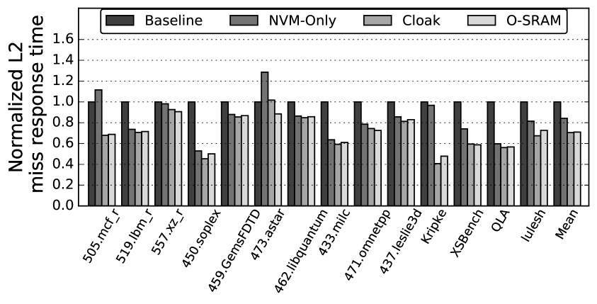
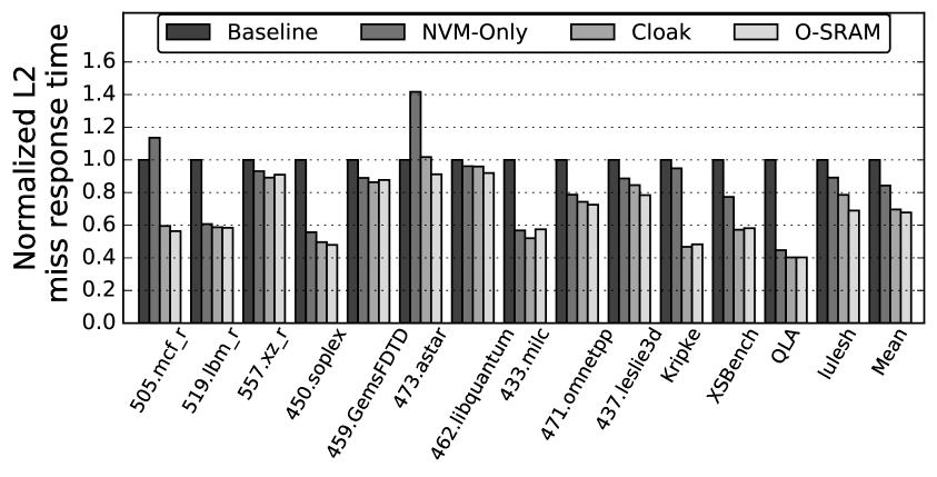
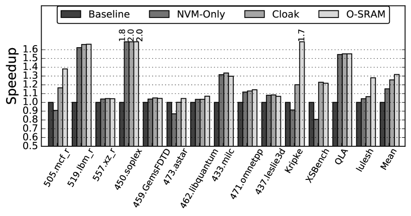
In this section, we evaluate the performance of Cloak. When replacing an SRAM-based cache with NVM, there are two factors that affect application performance. The first is the higher read and write latencies of NVM. The second is the lower cache miss rate due to the higher area density of NVM technology. We consider two different metrics in Figure 8 to show the performance impact of Cloak. Figures 8a and 8c show the sum of L2 miss response times for read CLRs, while Figures 8b and 8d depict the application speedup over the Baseline configuration. All figures are normalized to the Baseline configuration. We conducted experiments with a system that only utilizes 4KB pages, and with a system with Transparent Huge Pages enabled (2MB and 1GB pages).
Figures 8a and 8c show the sum of L2 miss response times for read CLRs, which we will call L2 miss response time. This time is calculated as the total number of cycles from issuing an L2 miss until the miss response reaches back to the L2. On average, Cloak reduces the L2 miss response time by 30.0% and 30.5% over Baseline, with and without Huge Pages. This impact is really close to that of the O-SRAM configuration. The NVM-Only configuration lowers the L2 miss response time by only 15.8% and 15.9%. It does not achieve the same reduction as Cloak or O-SRAM because of its higher and non-pipelined LLC hit latency. These results indicate that the PBs are effective at reducing the NVM cache read latency—practically as much as O-SRAM.
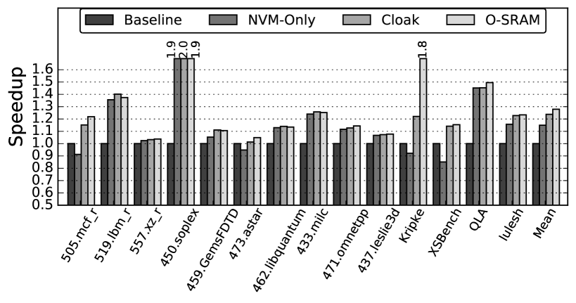
Figures 8b and 8d show the application speedup over Baseline. We see that NVM-Only LLCs can increase performance. The reason is the larger LLC capacity achieved via NVM technology, which can greatly decrease the LLC miss rate. However, there are benchmarks where NVM-Only experiences performance degradation compared to Baseline (505.mcf_r, 473.astar, Kripke, and XSBench), because the lower LLC miss rate cannot compensate for the higher LLC hit latency. Benchmarks with high L2 MPKI and high LLC hit rate suffer more from the increased read latency of an NVM-based LLC. For instance, 473.astar and XSBench with Huge Pages experience 13% and 19% lower performance than Baseline, respectively.
On the other hand, Cloak consistently attains higher performance than Baseline and NVM-Only. There are times when it even outperforms O-SRAM. This can happen for benchmarks with high PB hit rate because a PB hit has lower access latency than an SRAM-based LLC hit. This is due to the lower routing latency observed retrieving data from the PB data array compared to from a much larger SRAM-based LLC slice. On average, Cloak is 25.6% and 23.8% faster than Baseline with and without Huge Pages, respectively, while NVM-Only is 15.5% and 14.9% faster than Baseline. For some benchmarks, Cloak outperforms Baseline by up to 97%, effectively hiding the increased read latency of NVM.
We also tested Cloak’s efficacy by running mixes of four benchmarks. It can be shown that NVM-Only and Cloak outperform baseline by 24% and 31%, without Huge pages and by 27% and 33% with Huge pages, respectively. The rest of our evaluation focuses on a system that utilizes only 4KB pages due to space limitations. However, the performance trends remain the same when huge pages are enabled.
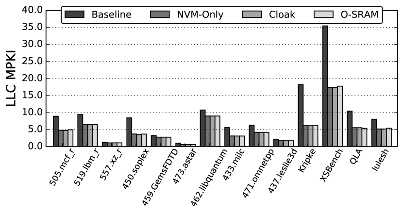
To further understand the performance impact of Cloak, we present two more performance metrics in Figures 9 and 10. In Figure 9, we show the drop in LLC Misses per Kilo-Instructions (MPKI) for the four configurations. The increased LLC capacity with NVM greatly reduces the MPKI of the applications. The MPKI decreases up to 55%, and drops across all benchmarks—including those with the highest MPKI such as XSBench (50% drop). In most cases, Cloak achieves an LLC MPKI close to that of O-SRAM.
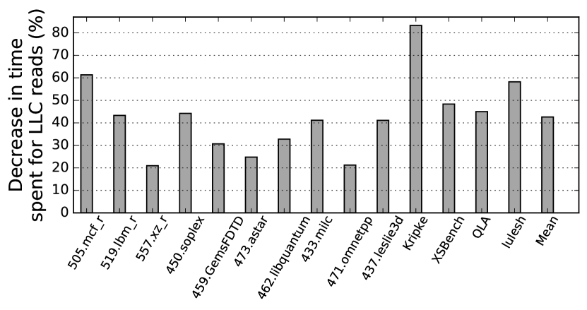
To isolate the performance impact of PBs, Figure 10 compares the total time that read requests spent in the LLC in NVM-Only and Cloak. This time is calculated as the total number of cycles from when an L2 miss is issued until the response is sent back to L2 from the LLC (in case of an LLC hit), or until the LLC declares a miss (in case of an LLC miss). Note that the two configurations have similar LLC MPKIs. Therefore, their cycle count difference depends on the PB hit rate in Cloak. Figure 10 shows that Cloak notably reduces these LLC read latency cycles and, therefore, accelerates the LLC read traffic. On average, LLC CLRs spent 42.5% less time in the LLC with Cloak than with NVM-Only. The PBs are able to speed-up Cloak because they service CLRs much faster than the LLC NVM-based data array. Moreover, when CLRs are serviced from the PBs, they do not block the LLC data array pipeline, giving the opportunity to subsequent CLRs that do not target PB-resident regions, to proceed in parallel. As a result, the PBs not only service requests faster but they also increase the overall throughput of the LLC cache.
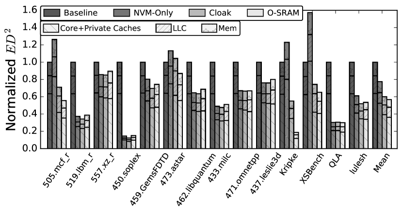
Figure 11 shows the of the different configurations normalized to Baseline. The bars are broken down into the contributions of the core plus private caches, the LLC, and main memory. Overall, we see that all the NVM designs have a lower than Baseline. On average, NVM-Only reduces the by 22.4%, while Cloak reduces it by 39.9%. The reasons are the lower execution times of the NVM configurations, the lower leakage power of the NVM cache (which is the main energy contributor of the LLC), and the reduced number of accesses to main memory. Compared to the NVM-Only design, it can be shown that Cloak consumes more energy in the LLC. This is because Cloak performs more tag checks and read accesses to the NVM data array to fetch data to the PBs, a Cloak request needs to check both the LLC and PB tags, and the PBs consume extra leakage power. However, this extra energy is compensated by a faster execution of Cloak because it services many requests from the PBs. O-SRAM reduces the by 43.3% over Baseline on average, delivering the best efficiency. However, we see that, in some cases, Cloak is better. O-SRAM has the same leakage power as baseline. So, in cases where the performance of O-SRAM cannot make up for its extra leakage, Cloak is better.
VII-B Cloak Characterization
To achieve high performance, it is crucial to maximize the use of PBs. In this section, we measure that 84.4% of the PTRs sent by Cloak to the LLC are for pages that have at least 6 cache lines in the LLC. Moreover, in 99% of the PTRs, we are able to find a PB to promote the lines.
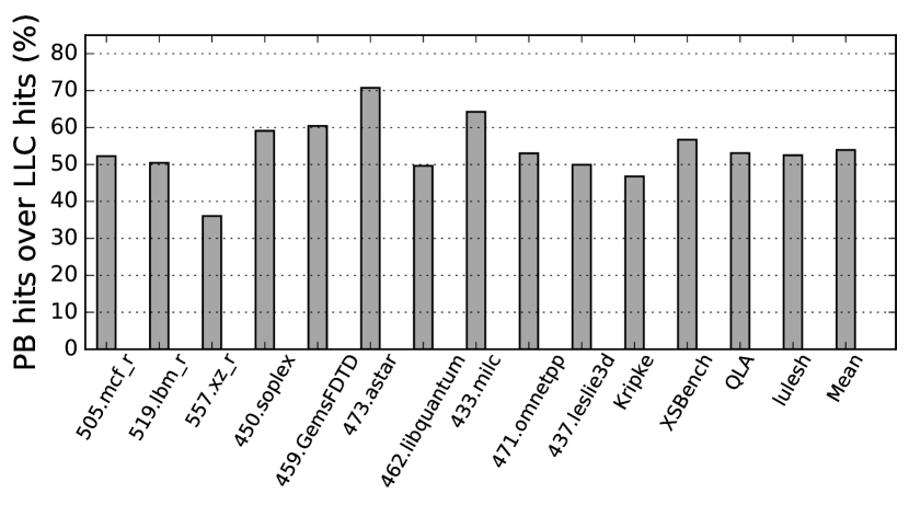
To get further insight, Figure 12 shows the percentage of LLC hits serviced from the PBs (instead of from the NVM data array). On average, 54% of the hit CLRs are serviced from the PBs instead of from the NVM data array. The benchmarks with the highest LLC hit traffic, such as XSBench (45 HPKI or Hits per Kilo-Instructions) and Kripke (32 HPKI) hit in the PB 57% and 48% of the time, respectively. This leads to substantial performance gains of Cloak over NVM-Only, as shown in Figure 8c.
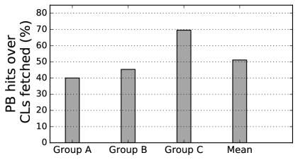
We now quantify the coverage of PTRs to the LLC in Figures 13a and 13b.333Group A, Group B, and Group C are the mean of the SPEC CPU® 2017, SPEC CPU® 2006, and Coral benchmarks of Table III, respectively. Figure 13a shows what percentage of the cache lines promoted into PBs are actually accessed from the PBs. We see that, on average, CLRs reference 51.1% of the cache lines promoted to the PBs. Cloak attains this high number by adopting a PB replacement algorithm that favors the victimization of PBs with few lines or a low number of hits. Note that when we promote cache lines into a PB, we do not pollute the LLC or L2. This is because the PBs simply hold a copy of the data present in the NVM data array.
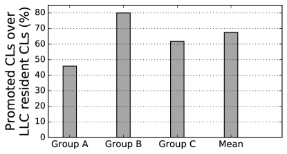
Figure 13b shows what percentage of the LLC-resident cache lines of a page are promoted to a PB in a PTR. This number is not 100% for two reasons. First, for a given page, some of the lines from different regions in the same physical row may conflict with each other, and cannot all be promoted to the PB. Second, if the number of LLC-resident lines is less than a threshold, Cloak does not promote the page. On average, Cloak promotes 68% of the LLC-resident cache lines to a PB—or about 26 lines.
VII-C Alternative Cloak Design
To further highlight the benefits of Cloak, we evaluate a scheme that fetches NVM-resident cache lines to the L2 cache instead of to the PBs, using the same trigger as Cloak. For this experiment, we keep the data layout we introduced for the NVM cache, so that we can identify the cache lines of a page with a single read operation. Moreover, as an optimization, we make sure that the L2 cache always prioritizes read requests from the core over prefetches from the LLC to the L2 cache. In addition, when the L2 MSHR entries are heavily utilized (i.e., 90%), we drop outstanding LLC-to-L2 prefetches.
We find that this design is not competitive with Cloak: on average, it is 19.8% slower than Cloak and increases the writes to NVM by 183%. This is because bulk prefetches from LLC to L2 saturate the interconnect, causing core requests to stall while arbitrating for the bus. Moreover, fetching many lines to L2 causes L2 thrashing, which in turn increases L2 misses. This is especially the case for benchmarks with high L2 MPKI such as XSBench. This benchmark takes 90% longer to complete with the new design than with Cloak because of the increased traffic between the L2 and the LLC. Only benchmarks with a small L2 MPKI and a high PB hit ratio, such as 450.soplex and 437.leslie3d, can benefit from this design, and attain a performance that is comparable to Cloak’s.
Similarly, an aggressive L2 prefetcher that tries to prefetch the same cache lines as Cloak faces the same performance bottleneck. Further, if the Cloak LLC data layout is not used, read requests from the core suffer from the low LLC read bandwidth resulting from the non-pipelined latency of NVM data array accesses.
VII-D Sensitivity Analysis
Finally, we perform two sensitivity analyses. First, we examine the sensitivity of Cloak to the LLC cache size, which is the primary parameter dictating the LLC hit/miss rate. Figures 14a and 14b show the average L2 miss response time and the average speedup, respectively, across all benchmarks, as the size of the LLC cache increases from 4MB to 32MB per core. All results are normalized to Baseline, which has an SRAM-based LLC with 4MB per core.
Figure 14a shows that the relative L2 miss response time drops with the increase in LLC size for all the schemes. Cloak has lower L2 miss response time than NVM-Only for all configurations. It has practically the same L2 miss response time as O-SRAM because the PBs provide even faster access than a larger SRAM LLC slice due to their smaller routing overhead.
Figure 14b shows that the speedup of all the schemes increases with the LLC size. This is because of the increasingly lower LLC miss rate. For all LLC sizes, Cloak delivers higher speedups than NVM-Only and lower speedups than O-SRAM. Interestingly, Cloak can tolerate the higher read latency of NVM and achieve equal performance as the Baseline already with a 4MB LLC.
We also analyze the effects of increasing the read latency of NVM LLC caches, while keeping the cache size at 16MB per core. Figure 15a and Figure 15b show the average L2 miss response time and the average speedup, respectively, across all benchmarks, as the LLC read latency is increased. We increase the latency by lengthening the NVM-based LLC data array read latency by 10, 20 and 30 cycles over the SRAM baseline. The configuration with +10 cycles represents the NVM cache we simulated in all of our prior experiments. All results are normalized to Baseline, which has an SRAM-based LLC of 4MB per core. The three designs represent an STT-RAM with a minimum read latency of 3 ns, 6 ns and 9 ns, respectively.
As the NVM LLC read latency increases, the relative L2 miss response time increases, and the speedup decreases. These trends occur for both NVM-Only and Cloak, although they are less prominent for Cloak. In all cases, Cloak has a lower L2 miss response time and a higher speedup than NVM-Only. This is because the PBs can tolerate part of the higher NVM array read latency. Even with an NVM with 30 cycles over the SRAM baseline, Cloak is faster than Baseline.
VIII Other Related Work
Page Caches. Prior work has looked into the use of die-stacked eDRAM as large LLCs [49, 26, 27, 28, 39, 37, 25, 62]. eDRAM-based caches are typically organized in pages instead of blocks to avoid massive tag storage. They are called Page Caches. When a request reaches a page cache and the page is not cached, the whole or a subset of the page [27, 26] is brought from main memory, generating off-chip traffic. Cloak does not generate any off-chip traffic. The capacity of page caches is underutilized, since a page allocates cache space even for lines that are not fetched. This reduces cache capacity. In addition, page caches add extra overhead to keep track of a page’s useful footprint. Cloak does not sacrifice any LLC capacity and does not need to track any footprint. Instead, it brings the LLC-resident lines into the PBs.
Page caches cannot be easily designed as victim or non-inclusive LLC caches—e.g., storing a victim line requires the allocation of space for the whole page. Instead, Cloak can be easily integrated with LLCs with different inclusion properties. Finally, if page caches are employed as an extra cache level (e.g., L4), Cloak can still replace the SRAM-based shared L3 in such a design.
Techniques to Hide High Latency. To hide the increased latency of NVM caches, in addition to the advanced techniques discussed in Section III, one can use conventional techniques such as prefetching and dead block elimination [8]. These proposals are orthogonal to Cloak and can be used in conjunction with it. However, LLC prefetchers incur increased complexity and can saturate memory bandwidth when using NVM caches [42, 59, 65]. The advantage of using the address translation hardware to make early decisions has been demonstrated before for page walks. Specifically, TEMPO [12] uses PTE page walk requests that miss in the cache hierarchy to prefetch from main memory to the LLC, the cache line that caused the page walk. PageSeer [34] uses page walk information to swap pages in a DRAM-NVM hybrid main memory system. Cloak is different from these approaches. First, it has a different target (i.e., the set of LLC-resident cache lines of a page); second, it uses a different trigger (i.e., TLB miss on a page used in the past).
IX Conclusion
This paper presented Cloak, a novel, low cost NVM LLC architecture that uses small SRAM-based page buffers to tolerate the higher and non-pipelined latency of NVM reads. An L1 TLB miss on certain pages triggers the data transfer of LLC-resident lines belonging to the page from the NVM LLC to the page buffers. The buffers will service subsequent requests for this page, and use a novel replacement algorithm to achieve high performance and low energy consumption. Cloak effectively hides the higher latency of NVM reads. On average, Cloak outperformed an SRAM LLC by 23.8% and an NVM-only LLC by 8.9%—in both cases, with negligible additional area. Further, the of Cloak was 39.9% and 17.5% lower, respectively, than these two designs.
References
- [1] “AMD64 Architecture Programmer’s Manual Volume 2: System Programming,” https://www.amd.com/system/files/TechDocs/24593.pdf.
- [2] “Apple A13 & Beyond: How Transistor Count And Costs Will Go Up,” https://wccftech.com/apple-5nm-3nm-cost-transistors/.
- [3] “Big trouble at 3nm,” https://semiengineering.com/big-trouble-at-3nm/.
- [4] “CORAL Benchmark Codes,” https://asc.llnl.gov/CORAL-benchmarks/.
- [5] “CORAL2 Benchmarks,” https://asc.llnl.gov/coral-2-benchmarks/.
- [6] “SPEC CPU2017,” https://www.spec.org/cpu2017.
- [7] H. M. Ahmed T. El-Thakeb, Hamdy A. Elhamid and Y. Ismail, “Performance evaluation of FINFET based SRAM under statistical VT variability,” in Proceedings of the 2014 International Conference on Microelectronics, ser. ICM’14. IEEE, 2014.
- [8] J. Ahn, S. Yoo, and K. Choi, “DASCA: Dead Write Prediction Assisted STT-RAM Cache Architecture,” in 2014 IEEE 20th International Symposium on High Performance Computer Architecture, Feb 2014.
- [9] J. G. Alzate, U. Arslan, P. Bai, J. Brockman, Y. J. Chen, N. Das, K. Fischer, T. Ghani, P. Heil, P. Hentges, R. Jahan, A. Littlejohn, M. Mainuddin, D. Ouellette, J. Pellegren, T. Pramanik, C. Puls, P. Quintero, T. Rahman, M. Sekhar, B. Sell, M. Seth, A. J. Smith, A. K. Smith, L. Wei, C. Wiegand, O. Golonzka, and F. Hamzaoglu, “2 MB Array-Level Demonstration of STT-MRAM Process and Performance Towards L4 Cache Applications,” in 2019 IEEE International Electron Devices Meeting (IEDM), 2019, pp. 2.4.1–2.4.4.
- [10] D. Apalkov, A. Khvalkovskiy, S. Watts, V. Nikitin, X. Tang, D. Lottis, K. Moon, X. Luo, E. Chen, A. Ong, A. Driskill-Smith, and M. Krounbi, “Spin-transfer Torque Magnetic Random Access Memory (STT-MRAM),” J. Emerg. Technol. Comput. Syst., May 2013.
- [11] R. Balasubramonian, A. B. Kahng, N. Muralimanohar, A. Shafiee, and V. Srinivas, “CACTI 7: New Tools for Interconnect Exploration in Innovative Off-Chip Memories,” ACM Trans. Archit. Code Optim., vol. 14, no. 2, Jun. 2017. [Online]. Available: http://doi.acm.org/10.1145/3085572
- [12] A. Bhattacharjee, “Translation-Triggered Prefetching,” in the Twenty-Second International Conference on Architectural Support for Programming Languages and Operating Systems, 2017.
- [13] N. Chachmon, D. Richins, R. Cohn, M. Christensson, W. Cui, and V. J. Reddi, “Simulation and Analysis Engine for Scale-Out Workloads,” in 2016 International Conference on Supercomputing, 2016.
- [14] M. Chang, P. Rosenfeld, S. Lu, and B. Jacob, “Technology comparison for large last-level caches (L3Cs): Low-leakage SRAM, low write-energy STT-RAM, and refresh-optimized eDRAM,” in 2013 IEEE 19th International Symposium on High Performance Computer Architecture (HPCA), 2013.
- [15] Y. Chen, J. Cong, H. Huang, B. Liu, C. Liu, M. Potkonjak, and G. Reinman, “Dynamically reconfigurable hybrid cache: An energy-efficient last-level cache design,” in 2012 Design, Automation Test in Europe Conference Exhibition (DATE), 2012.
- [16] Y. Chen, H. Li, X. Wang, W. Zhu, W. Xu, and T. Zhang, “A 130 nm 1.2 V/3.3 V 16 Kb Spin-Transfer Torque Random Access Memory With Nondestructive Self-Reference Sensing Scheme,” IEEE Journal of Solid-State Circuits, Feb 2012.
- [17] H. Cheng, J. Zhao, J. Sampson, M. J. Irwin, A. Jaleel, Y. Lu, and Y. Xie, “LAP: Loop-Block Aware Inclusion Properties for Energy-Efficient Asymmetric Last Level Caches,” in 2016 ACM/IEEE 43rd Annual International Symposium on Computer Architecture (ISCA), 2016.
- [18] Y. Chih, Y. Shih, C. Lee, Y. Chang, P. Lee, H. Lin, Y. Chen, C. Lo, M. Shih, K. Shen, H. Chuang, and T. J. Chang, “13.3 A 22nm 32Mb Embedded STT-MRAM with 10ns Read Speed, 1M Cycle Write Endurance, 10 Years Retention at 150°C and High Immunity to Magnetic Field Interference,” in 2020 IEEE International Solid- State Circuits Conference - (ISSCC), 2020, pp. 222–224.
- [19] A. Chintaluri, H. Naeimi, S. Natarajan, and A. Raychowdhury, “Analysis of Defects and Variations in Embedded Spin Transfer Torque (STT) MRAM Arrays,” IEEE Journal on Emerging and Selected Topics in Circuits and Systems, Sep. 2016.
- [20] Greg Hamerly and E. Perelman and Jeremy Lau and B. Calder, “SimPoint 3.0: Faster and More Flexible Program Phase Analysis,” J. Instr. Level Parallelism, vol. 7, 2005.
- [21] S. Gupta and H. Zhou, “Spatial Locality-Aware Cache Partitioning for Effective Cache Sharing,” in 2015 44th International Conference on Parallel Processing, Sep. 2015.
- [22] J. L. Henning, “SPEC CPU2006 Benchmark Descriptions,” SIGARCH Comput. Archit. News, vol. 34, no. 4, Sep. 2006. [Online]. Available: http://doi.acm.org/10.1145/1186736.1186737
- [23] K. Ikegami, H. Noguchi, S. Takaya, C. Kamata, M. Amano, K. Abe, K. Kushida, E. Kitagawa, T. Ochiai, N. Shimomura, D. Saida, A. Kawasumi, H. Hara, J. Ito, and S. Fujita, “MTJ-based ”normally-off processors” with thermal stability factor engineered perpendicular MTJ, L2 cache based on 2T-2MTJ cell, L3 and last level cache based on 1T-1MTJ cell and novel error handling scheme,” in 2015 IEEE International Electron Devices Meeting (IEDM), 2015, pp. 25.1.1–25.1.4.
- [24] G. Jan, L. Thomas, S. Le, Y. Lee, H. Liu, J. Zhu, R. Tong, K. Pi, Y. Wang, D. Shen, R. He, J. Haq, J. Teng, V. Lam, K. Huang, T. Zhong, T. Torng, and P. Wang, “Demonstration of fully functional 8Mb perpendicular STT-MRAM chips with sub-5ns writing for non-volatile embedded memories,” in 2014 Symposium on VLSI Technology (VLSI-Technology), June 2014.
- [25] H. Jang, Y. Lee, J. Kim, Y. Kim, J. Kim, J. Jeong, and J. W. Lee, “Efficient footprint caching for Tagless DRAM Caches,” in 2016 IEEE International Symposium on High Performance Computer Architecture, 2016, pp. 237–248.
- [26] D. Jevdjic, G. H. Loh, C. Kaynak, and B. Falsafi, “Unison Cache: A Scalable and Effective Die-Stacked DRAM Cache,” in 2014 47th Annual IEEE/ACM International Symposium on Microarchitecture, 2014, pp. 25–37.
- [27] D. Jevdjic, S. Volos, and B. Falsafi, “Die-Stacked DRAM Caches for Servers: Hit Ratio, Latency, or Bandwidth? Have It All with Footprint Cache,” in Proceedings of the 40th Annual International Symposium on Computer Architecture, ser. ISCA ’13. New York, NY, USA: Association for Computing Machinery, 2013, p. 404–415. [Online]. Available: https://doi.org/10.1145/2485922.2485957
- [28] X. Jiang, N. Madan, L. Zhao, M. Upton, R. Iyer, S. Makineni, D. Newell, Y. Solihin, and R. Balasubramonian, “CHOP: Adaptive filter-based DRAM caching for CMP server platforms,” in HPCA - 16 2010 The Sixteenth International Symposium on High-Performance Computer Architecture, 2010, pp. 1–12.
- [29] A. Jog, A. K. Mishra, C. Xu, Y. Xie, V. Narayanan, R. Iyer, and C. R. Das, “Cache revive: Architecting volatile STT-RAM caches for enhanced performance in CMPs,” in DAC Design Automation Conference, 2012.
- [30] D. Kang, S. Baek, J. Choi, D. Lee, S. H. Noh, and O. Mutlu, “Amnesic cache management for non-volatile memory,” in 2015 31st Symposium on Mass Storage Systems and Technologies (MSST), 2015, pp. 1–13.
- [31] E. Karl, Z. Guo, J. Conary, J. Miller, Y. Ng, S. Nalam, D. Kim, J. Keane, X. Wang, U. Bhattacharya, and K. Zhang, “A 0.6 V, 1.5 GHz 84 Mb SRAM in 14 nm FinFET CMOS Technology With Capacitive Charge-Sharing Write Assist Circuitry,” IEEE Journal of Solid-State Circuits, vol. 51, no. 1, pp. 222–229, 2016.
- [32] T. Kawahara, R. Takemura, K. Miura, J. Hayakawa, S. Ikeda, Y. Lee, R. Sasaki, Y. Goto, K. Ito, T. Meguro, F. Matsukura, H. Takahashi, H. Matsuoka, and H. Ohno, “2Mb Spin-Transfer Torque RAM (SPRAM) with Bit-by-Bit Bidirectional Current Write and Parallelizing-Direction Current Read,” in 2007 IEEE International Solid-State Circuits Conference, Feb 2007.
- [33] A. V. Khvalkovskiy, D. Apalkov, S. Watts, R. Chepulskii, R. S. Beach, A. Ong, X. Tang, A. Driskill-Smith, W. H. Butler, P. B. Visscher, D. Lottis, E. Chen, V. Nikitin, and M. Krounbi, “Basic principles of STT-MRAM cell operation in memory arrays,” Journal of Physics D: Applied Physics, feb 2013.
- [34] A. Kokolis, D. Skarlatos, and J. Torrellas, “PageSeer: Using Page Walks to Trigger Page Swaps in Hybrid Memory Systems,” in 2019 IEEE 25th International Symposium on High Performance Computer Architecture, Feb 2019.
- [35] A. Kolli, J. Rosen, S. Diestelhorst, A. Saidi, S. Pelley, S. Liu, P. M. Chen, and T. F. Wenisch, “Delegated Persist Ordering,” in The 49th Annual IEEE/ACM International Symposium on Microarchitecture, 2016.
- [36] K. Korgaonkar, I. Bhati, H. Liu, J. Gaur, S. Manipatruni, S. Subramoney, T. Karnik, S. Swanson, I. Young, and H. Wang, “Density Tradeoffs of Non-Volatile Memory as a Replacement for SRAM Based Last Level Cache,” in 2018 ACM/IEEE 45th Annual International Symposium on Computer Architecture, June 2018.
- [37] Y. Lee, J. Kim, H. Jang, H. Yang, J. Kim, J. Jeong, and J. W. Lee, “A fully associative, tagless DRAM cache,” in 2015 ACM/IEEE 42nd Annual International Symposium on Computer Architecture, 2015, pp. 211–222.
- [38] S. Li, J. H. Ahn, R. D. Strong, J. B. Brockman, D. M. Tullsen, and N. P. Jouppi, “McPAT: An Integrated Power, Area, and Timing Modeling Framework for Multicore and Manycore Architectures,” in Proceedings of the 42nd Annual IEEE/ACM International Symposium on Microarchitecture, 2009, pp. 469–480.
- [39] G. H. Loh and M. D. Hill, “Efficiently enabling conventional block sizes for very large die-stacked dram caches,” in 2011 44th Annual IEEE/ACM International Symposium on Microarchitecture, 2011, pp. 454–464.
- [40] Y. Lu, T. Zhong, W. Hsu, S. Kim, X. Lu, J. J. Kan, C. Park, W. C. Chen, X. Li, X. Zhu, P. Wang, M. Gottwald, J. Fatehi, L. Seward, J. P. Kim, N. Yu, G. Jan, J. Haq, S. Le, Y. J. Wang, L. Thomas, J. Zhu, H. Liu, Y. J. Lee, R. Y. Tong, K. Pi, D. Shen, R. He, Z. Teng, V. Lam, R. Annapragada, T. Torng, P. Wang, and S. H. Kang, “Fully functional perpendicular STT-MRAM macro embedded in 40 nm logic for energy-efficient IOT applications,” in 2015 IEEE International Electron Devices Meeting (IEDM), Dec 2015.
- [41] P. S. Magnusson, M. Christensson, J. Eskilson, D. Forsgren, G. Hallberg, J. Hogberg, F. Larsson, A. Moestedt, and B. Werner, “Simics: A full system simulation platform,” Computer, vol. 35, no. 2, pp. 50–58, Feb 2002.
- [42] M. Mao, G. Sun, Y. Li, A. K. Jones, and Y. Chen, “Prefetching techniques for STT-RAM based last-level cache in CMP systems,” in 2014 19th Asia and South Pacific Design Automation Conference, Jan 2014.
- [43] H. Noguchi, K. Ikegami, K. Kushida, K. Abe, S. Itai, S. Takaya, N. Shimomura, J. Ito, A. Kawasumi, H. Hara, and S. Fujita, “A 3.3ns-access-time 71.2W/MHz 1Mb embedded STT-MRAM using physically eliminated read-disturb scheme and normally-off memory architecture,” in 2015 IEEE International Solid-State Circuits Conference, Feb 2015.
- [44] H. Noguchi, K. Ikegami, N. Shimomura, T. Tetsufumi, J. Ito, and S. Fujita, “Highly reliable and low-power nonvolatile cache memory with advanced perpendicular STT-MRAM for high-performance CPU,” in 2014 Symposium on VLSI Circuits, June 2014.
- [45] H. Noguchi, K. Ikegami, S. Takaya, E. Arima, K. Kushida, A. Kawasumi, H. Hara, K. Abe, N. Shimomura, J. Ito, S. Fujita, T. Nakada, and H. Nakamura, “4Mb STT-MRAM-based cache with memory-access-aware power optimization and write-verify-write / read-modify-write scheme,” in 2016 IEEE International Solid-State Circuits Conference, Jan 2016.
- [46] T. Ohsawa, H. Koike, S. Miura, H. Honjo, K. Kinoshita, S. Ikeda, T. Hanyu, H. Ohno, and T. Endoh, “A 1 Mb Nonvolatile Embedded Memory Using 4T2MTJ Cell With 32 b Fine-Grained Power Gating Scheme,” IEEE Journal of Solid-State Circuits, June 2013.
- [47] T. Ohsawa, S. Miura, K. Kinoshita, H. Honjo, S. Ikeda, T. Hanyu, H. Ohno, and T. Endoh, “A 1.5nsec/2.1nsec random read/write cycle 1Mb STT-RAM using 6T2MTJ cell with background write for nonvolatile e-memories,” in 2013 Symposium on VLSI Circuits, June 2013.
- [48] S. Pelley, P. M. Chen, and T. F. Wenisch, “Memory Persistency,” in Proceeding of the 41st Annual International Symposium on Computer Architecuture, 2014.
- [49] M. K. Qureshi and G. H. Loh, “Fundamental latency trade-off in architecting dram caches: Outperforming impractical sram-tags with a simple and practical design,” in 2012 45th Annual IEEE/ACM International Symposium on Microarchitecture, 2012, pp. 235–246.
- [50] M. K. Qureshi, S. Gurumurthi, and B. Rajendran, Phase Change Memory: From Devices to Systems, 1st ed. Morgan & Claypool Publishers, 2011.
- [51] A. F. Rodrigues, K. S. Hemmert, B. W. Barrett, C. Kersey, R. Oldfield, M. Weston, R. Risen, J. Cook, P. Rosenfeld, E. CooperBalls, and B. Jacob, “The Structural Simulation Toolkit,” SIGMETRICS Perform. Eval. Rev., vol. 38, no. 4, Mar. 2011.
- [52] P. Rosenfeld, E. Cooper-Balis, and B. Jacob, “DRAMSim2: A Cycle Accurate Memory System Simulator,” IEEE Computer Architecture Letters, Jan 2011.
- [53] S. Sakhare, M. Perumkunnil, T. H. Bao, S. Rao, W. Kim, D. Crotti, F. Yasin, S. Couet, J. Swerts, S. Kundu, D. Yakimets, R. Baert, H. Oh, A. Spessot, A. Mocuta, G. S. Kar, and A. Furnemont, “Enablement of STT-MRAM as last level cache for the high performance computing domain at the 5nm node,” in 2018 IEEE International Electron Devices Meeting (IEDM), 2018, pp. 18.3.1–18.3.4.
- [54] A. Shafaei, Y. Wang, X. Lin, and M. Pedram, “Fincacti: Architectural analysis and modeling of caches with deeply-scaled finfet devices,” in 2014 IEEE Computer Society Annual Symposium on VLSI, 2014, pp. 290–295.
- [55] C. W. Smullen, V. Mohan, A. Nigam, S. Gurumurthi, and M. R. Stan, “Relaxing non-volatility for fast and energy-efficient STT-RAM caches,” in 2011 IEEE 17th International Symposium on High Performance Computer Architecture, Feb 2011.
- [56] S. S.R., B. Ramakrishna, Samiksha, R. Banu, and P. Shubham, “Design and Performance Analysis of 6T SRAM Cell in 22nm CMOS and FINFET Technology Nodes,” in Proceedings of the 2017 International Conference on Recent Advances in Electronics and Communication Technology, ser. ICRAECT’17. IEEE, 2017.
- [57] G. Sun, X. Dong, Y. Xie, J. Li, and Y. Chen, “A novel architecture of the 3D stacked MRAM L2 cache for CMPs,” in 2009 IEEE 15th International Symposium on High Performance Computer Architecture, 2009.
- [58] Z. Sun, X. Bi, H. Li, W. Wong, Z. Ong, X. Zhu, and W. Wu, “Multi retention level STT-RAM cache designs with a dynamic refresh scheme,” in 2011 44th Annual IEEE/ACM International Symposium on Microarchitecture, Dec 2011.
- [59] J. Wang, X. Dong, and Y. Xie, “OAP: An obstruction-aware cache management policy for STT-RAM last-level caches,” in 2013 Design, Automation Test in Europe Conference Exhibition, March 2013.
- [60] Z. Wang, X. Hao, P. Xu, L. Hu, D. Jung, W. Kim, K. Satoh, B. Yen, Z. Wei, L. Wang, J. Zhang, and Y. Huai, “Stt-mram for embedded memory applications,” in 2020 IEEE International Memory Workshop (IMW), 2020, pp. 1–3.
- [61] Z. Wang, D. A. Jimenez, C. Xu, G. Sun, and Y. Xie, “Adaptive placement and migration policy for an STT-RAM-based hybrid cache,” in 2014 IEEE 20th International Symposium on High Performance Computer Architecture, Feb 2014.
- [62] D. H. Woo, N. H. Seong, D. L. Lewis, and H.-H. S. Lee, “An optimized 3d-stacked memory architecture by exploiting excessive, high-density tsv bandwidth,” in HPCA - 16 2010 The Sixteenth International Symposium on High-Performance Computer Architecture, 2010, pp. 1–12.
- [63] X. Wu, J. Li, L. Zhang, E. Speight, R. Rajamony, and Y. Xie, “Hybrid Cache Architecture with Disparate Memory Technologies,” in Proceedings of the 36th Annual International Symposium on Computer Architecture, 2009.
- [64] W. Xu, H. Sun, X. Wang, Y. Chen, and T. Zhang, “Design of Last-Level On-Chip Cache Using Spin-Torque Transfer RAM (STT RAM),” IEEE Transactions on Very Large Scale Integration Systems, March 2011.
- [65] J. Zhan, O. Kayiran, G. H. Loh, C. R. Das, and Y. Xie, “OSCAR: Orchestrating STT-RAM cache traffic for heterogeneous CPU-GPU architectures,” in 2016 49th Annual IEEE/ACM International Symposium on Microarchitecture, Oct 2016.
- [66] L. Zhang, B. Neely, D. Franklin, D. Strukov, Y. Xie, and F. T. Chong, “Mellow Writes: Extending Lifetime in Resistive Memories through Selective Slow Write Backs,” in 2016 ACM/IEEE 43rd Annual International Symposium on Computer Architecture, 2016.
- [67] Y. Zhang, Y. Li, Z. Sun, H. Li, Y. Chen, and A. K. Jones, “Read Performance: The Newest Barrier in Scaled STT-RAM,” IEEE Transactions on Very Large Scale Integration Systems, June 2015.