Transformation of an energy spectrum and wave functions in the crossover from two- to three-dimensional topological insulator in HgTe quantum wells: long and thorny way
Abstract
A magnetotransport and quantum capacitance of the two-dimensional electron gas in HgTe/CdxHg1-xTe quantum wells of a width () nm are experimentally investigated. It is shown that the first energy subband of spatial quantization is split due to the spin-orbit interaction and the split branches are single-spin, therewith the splitting strength increases with the increase of the quantum well width. The electron effective masses in the branches are close to each other within the actual density range. Magneto-intersubband oscillations (MISO) observed in the structures under study exhibit the growing amplitude with the increasing electron density that contradicts to the expected decrease of wave function overlap for the rectangular quantum well. To interpret the data obtained, we have used a self-consistent approach to calculate the electron energy spectrum and the wave function within framework of the kP-model. It has been in particular shown that the MISO amplitude increase results from the increasing overlap of the wave functions due to their shift from the gate electrode with the gate voltage increase known as phenomenon of the negative electron polarizability. The results obtained from the transport experiments are supported by quantum capacitance measurements.
pacs:
73.20.Fz, 73.21.Fg, 73.63.HsI Introduction
Structures with HgTe quantum wells (QWs) are attracting a lot of attention for many reasons. First, the QW is a gapless semiconductor, while the barriers Hg1-xCdxTe are a semiconductor with a normal band ordering [1, 2].
Second, the band spectra of the parent materials HgTe and Hg1-xCdxTe have been studied in detail and their parameters are fairly well known.
Third, the electron energy spectrum of the HgTe-based quantum wells is calculated within framework of the kP theory in numerous papers (see, e.g., [3, 4, 5, 6, 7, 8] and references therein). It is shown that different types of spectrum are realized depending on the QW width (). At nm it is gapless [3] and close to the linear Dirac-like spectrum at small quasimomentum [6]. When QW is narrow, , the ordering of energy subbands of spatial quantization is analogous to that in conventional semiconductors; the highest valence subband at is formed from the heavy hole states, while the lowest conduction subband is formed both from the states and light hole states. For a thicker HgTe layer, , the quantum well is in the inverted regime; the lowest conduction subband is formed from the heavy hole states [9], whereas the subband formed from the states and light hole states sinks into the valence band. In the inverted regime, the spectrum becomes semimetallic when nm.
Fourth, the theory predicts that at nm, the QW will be a two-dimensional topological insulator when, along with two-dimensional states, one-dimensional edge states are formed. And when is greater than nm it will be a three-dimensional topological insulator, when, along with two-dimensional states, two-dimensional, single-spin surface states are formed with a characteristic localization length in the direction less than the QW width, where is direction perpendicular to the QW plane.
And finally, when is much larger than nm, we obtain HgTe film with three-dimensional states and two-dimensional single-spin surface states.
In addition, the technology of growing HgTe/Hg1-xCdxTe structures is well developed [10, 11, 12] which makes it possible to grow structures with high mobility electrons and holes. Multiband -calculations of the spectrum and wave functions are well developed and tested. This would seem to make it possible to understand in all the properties (transport, optical, etc.) of such structures.
Experimentally, the energy spectrum of structures with nm detail has been studied in sufficient detail by various techniques including the optical and photoelectric methods in a wide range of radiation wavelength, starting from the terahertz range [13, 14, 15, 16], magnetotransport [17, 18, 19, 20, 21]. It was shown that in general the energy spectrum is reasonably described within the framework of the kP model, in which the spin-orbit (SO) interaction is taken into account. The main contribution to SO interaction comes from the asymmetry of the interfaces for the valence band [22, 23] and from the Bychkov-Rashba effect for the conduction band [4, 24]. But some discrepancies remain: the effective mass of electrons at the bottom of the conduction band at thicknesses nm turns out to be times less than the theoretical one (the authors of Ref. [2] assume that this is due to many-particle effects).
Many papers have been devoted to the study of conductivity by the edge states [25, 26, 27, 28], which should be topologically protected from back scattering according to theoretical predictions [29, 30, 31, 32]. However, in most experiments, the mean free path for such states did not exceed m, which is not much greater than the mean free path of two-dimensional electrons () in these structures [for 2D systems with cm2/Vs, cm-2, m]. Another prediction of the theory concerns the features of the spectrum and wave functions in wide HgTe quantum wells. It was predicted [33] that “single-spin” surface states should exist in sufficiently wide quantum wells, which are well localized at the boundaries of the quantum well. Studies of such structures have attracted a lot of attention of experimenters [34, 19, 35, 36]. Structures with a QW width of nm were mainly studied. Only the phenomenological model of surface states was used to interpret the data. No quantitative comparison with theoretical calculations was made.
What are the specific features of the methods used to study the spectrum, its transformation with increasing width, the properties of states caused by a nontrivial topology: “edge” and “surface”?
In interband optics and magneto-optics experiments, both the valence band and the conduction band participate in the processes. But the valence band has a complex spectrum, which makes it difficult to interpret experimental data.
When studying the low-temperature transport, one studies the spectrum at the Fermi level. The Fermi energy can be easily changed, if you are investigating gated structures by changing the gate voltage (). But in this case, the gate voltage changes not only the carrier density, and hence the Fermi energy, but also the potential profile of QW. To interpret the results in this case, it is necessary to solve the self-consistent problem taking into account the real potential, which changes significantly with a change of the gate voltage.
In principle, the Fermi energy can be changed by doping, but even in this case, it is imperative to take into account the electrostatic potential of the charge carriers and the doping impurities, i.e., to solve a self-consistent problem when interpreting the data quantitatively. In addition, these will be different samples, the asymmetry of which is difficult to determine and change.
In almost all the experimental studies of the magnetotransport in wide QWs ( nm), structures with the gate were studied, and the results were analyzed using an “intuitive model” in which it is assumed that near each of the walls there are single-spin states at a some distance from the wall of a some width , which are independent of and shift only in the energy by applied gate voltage [37, 21, 38]. The accuracy of this approach, especially for sufficiently wide QWs, remains unclear.
| structure | (nm) | (cm | (cm2/Vs) | (cm-2) | (cm-2) |
|---|---|---|---|---|---|
| 110614 | |||||
| 180820 | |||||
| 180824 | |||||
| 180823 |
To understand how the energy spectrum and wave functions of states change with an increase in the QW width, in this work we have experimentally studied the magnetotransport phenomena and the dependence of the capacitance between 2D gas and the gate electrode in a wide range of gate voltages in practically unexplored QWs of () nm width. When analyzing the results, we used self-consistent calculations of the energy spectrum carried out within the framework of the four-band kP model.
II The structures investigated
Our HgTe quantum wells were realized on the basis of HgTe/Hg1-xCdxTe () heterostructure grown by molecular beam epitaxy on GaAs substrate with the (013) surface orientation [11]. The nominal widths of the quantum wells under study were nm. The samples were mesa etched into standard Hall bars of mm width with the distance between the potential probes of mm. To change and control the electron and hole densities ( and , respectively) in the quantum well, the field-effect transistors were fabricated with parylene as an insulator and aluminum as a gate electrode. The measurements were performed in the DC regime of linear response at temperatures K in the magnetic field up to T. For each heterostructure, several samples were fabricated and studied. The parameters of the structures investigated are presented in the Table 1.
The main results for all the structures investigated are qualitatively close to each other, therefore, as an example, let us consider in more detail the data obtained for the structure with nm, for which all the features manifest themselves more clearly.
For a general characterization of the structure, let us consider first the gate voltage dependences of the electrons and holes over entire range of . When V, only electrons participate in the conductivity, the Hall resistance at low magnetic field ( T) linearly depends on , and the Hall electron density , where and stand for elementary charge and the Hall coefficient, respectively, increases linearly with the increase [Fig. 1(a)]. When V, the Hall coefficient strongly depends on , changing sign from electronic at low to hole-like with increasing , and at the same time increases strongly with [see insets in Fig. 1(a)]. Within this gate voltage range the electron and hole densities were found by simultaneous fit of dependences and at T within classical model of the conductivity by two types of the carriers. Fig. 1(a) shows that total charge of free carriers in QW linearly depends on as , cm-2 within whole range. Note that the absolute value of the slope of this dependence cm-2V-1 is in a good agreement with that obtained from the capacitance measurements , where is the capacitance between the 2D gas and the gate electrode, measured for the same structure, is the gated area.
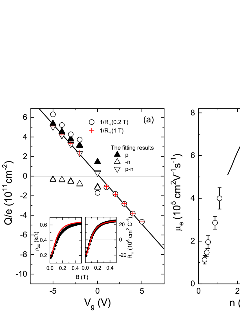
Fig. 1(b) shows the electron density dependencies of electron mobility at V when electrons exist together with hole (circles) and at V when only electrons contributes to the conductivity (the curve). It seen that the dependence of the mobility is non-monotonic. It increases with increase while cm-2 and shows a sharp decrease at higher values of resulting from the beginning of filling the second subband of spatial quantization [see Table 1 and Fig. 4(b)].
III Spin-orbit splitting of conduction band. Experiment
The aim of this paper is to study the spectrum and wave functions of electrons in the conduction band, therefore, below we will discuss the results only for . The spectrum of the valence band is much more complicated and should be discussed in a separate paper.
As example, the magnetic field dependences of and oscillating part of resistivity , where is the monotonic part of , for some gate voltages are presented in Fig. 2(a) and 2(b), respectively. As seen, linearly increases with in low magnetic fields, then the oscillations appear, which are transformed to the steps of the quantum Hall effect in the higher magnetic field.
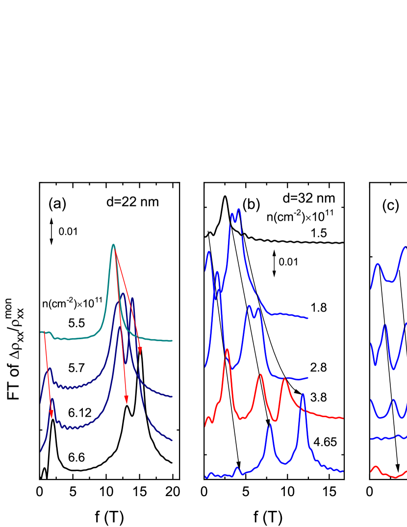
The Fourier spectra of found in magnetic field range before onset of the steps of the quantum Hall effect are presented in Fig. 2(c). These data show that unsplit oscillations with one component in the Fourier spectrum is observed for low electron density cm-2. With increasing , it splits into two and components, and a low-frequency component appears.

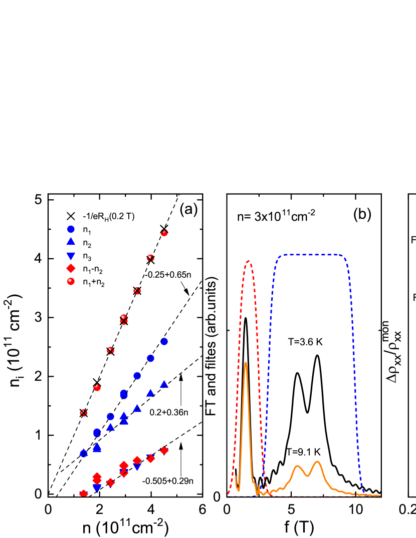
At cm-2, the electron densities corresponding to each Fourier component are plotted in Fig. 3(a) assuming that these states are non-degenerate. It can be seen that the sum of the two high-frequency components gives a density that coincides with the Hall density. The difference coincides with the low-frequency component . This is consistent with the following interpretation: (i) the high frequency components and corresponds to two single-spin branches of the first spatially quantized subband split due to SO interaction, the splitting value increases with increasing gate voltage; (ii) the low frequency component arises from the transitions between split branches which result in the well-known magneto-intersubband oscillations (MISO). This interpretation is confirmed by the temperature dependence of the amplitudes of these Fourier components shown in Fig. 3(b). It is seen that the amplitude of the two high-frequency components corresponding to the Shubnikov-de Haas (SdH) oscillations of each of the spectrum branches decreases strongly with increasing temperature, while the MISO amplitude decreases insignificantly, as predicted theoretically [39, 40].
Figure 3(a) shows that the electron densities in the split branches within experimental uncertainty are well described by the linear dependences with the different slopes equal to and . These lines intersect at the point cm-2. Therefore, we believe that the quantum well is close to symmetric one at cm-2.
To compare the results obtained for the structures with the different QW widths, we will characterize the “strength” of spin-orbit splitting by the phenomenological parameter 111This is of course an approximation. In the paper [24] we show that the theory predicts nonlinear dependences and at the small splitting values. However, in order to trace the change in spin-orbit splitting with the change, such a SOS parameter is suitable.. In Fig. 4(a), we plot the dependences of SOS for all the structures from the Table 1 and for the structures investigated in Ref. [24]. As seen the SOS value monotonically, without inflection, increases with the increasing QW width over the entire range. This shows that no new strongly localized “surface” states arise up up to nm at least.
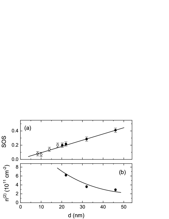
Another parameter that can be extracted from the analysis of the SdH oscillations is the electron density at which the second subband of the spatial quantization begins to be occupied. As seen from Fig. 4(b) the values diminish with increase monotonically that as shown in Section VI agrees satisfactorily with the theoretical results.
Thus, all the results presented above show that the main magnetotransport properties of wide QWs are qualitatively similar to that previously investigated in QWs with a width of nm.
IV Electron masses in the branches
To to separate the SdH oscillation components corresponding to split branches and obtain the masses in them, we used of bandpass filtering as shown in Fig. 3(b). To improve the resolution of the Fourier spectra, the oscillating part of was multiplied by . Then, applying the inverse Fourier transformation we obtained the oscillations of the frequency [the curve F3 in Fig. 3(c)] and superposition of oscillations with two higher frequencies and [the curve labeled as F1+F2 in Fig. 3(c)]. To keep the correct ratio of the amplitudes of the different oscillations, the curves obtained after the inverse Fourier transform were multiplied by . Fitting the curve F1+F2 by the sum of the two Lifshits-Kosevich (LK) formulas [42] allows us to separate the contributions which are presented by the curves F1 and F2 in this figure (for more detail see Ref. [43]). This method of decomposition allows us not only to reliably separate out the contributions of each of the three oscillation components and determine their frequencies, but also to determine the amplitudes. Applying this procedure to analyse the oscillations measured for different temperatures one can be obtain the temperature dependences of the amplitudes of the oscillations coming from the branches and hence obtain the cyclotron effective mass at the Fermi energy for each of these branches.
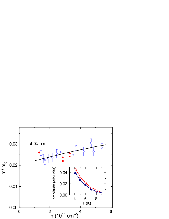
The inset in Fig. 5 shows the temperature dependences of the amplitudes of the SdH oscillation components for T separated as described above for the total electron density cm-2. It is seen that the temperature dependences of the amplitudes are very close to each other. They are well fitted by the LK formula that gives the values of effective masses and for the electron densities in the branches equal to cm-2 and cm-2, respectively. These values and the values obtained for the other electron densities are shown in Fig. 5 by squares and triangles. As seen the effective masses in the spin-orbit splitting branches are very close to each other.
We attract here the reader’s attention to a peculiarity of MISO in HgTe-based QWs already discussed in Ref. [43] for the narrower quantum wells. Fig. 3(c) shows that beating of the SdH oscillations results as a sum of two high-frequency components. As seen the magnetic fields of the antinodes of high-frequency oscillations correspond to the minima in -MISO. Such a mutual position is opposite to that observed in ordinary structures, namely, in double and wide quantum wells. But it agrees with that observed in narrow HgTe- and InxGa1-xAs-based QWs, in which the splitting of oscillation arises due to spin-orbit splitting. The authors of Ref. [43] assume that the unusual mutual positions of the MISO extrema and the SdH oscillation antinodes originate from the dependence of the probability of transitions between the Landau levels of different branches on the difference in their energies.
Let us consider the data obtained by the other method which gives the effective mass over a wide electron density range. It consists in analysing the temperature dependence of the amplitude of the oscillations of the vs dependences in a fixed magnetic field. This method gives an average of the effective masses in the branches. The results are shown in Fig. 5 by circles. It is seen that the results obtained by the two methods practically coincide. The effective masses increase slightly with an increase in the total electron concentration from at cm-2 to at cm-2.
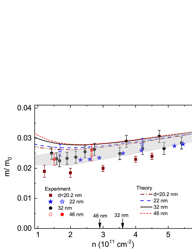
The same measurements and analyses were carried out for all the structures under study. The results are shown in Fig. 6. It is seen that effective masses QWs with nm are close to each other over the whole electron density range. They are within the shadow area which width is comparable with the experimental errors. In the same figure, we plot the theoretical dependences calculated within the framework of the standard kP model for the rectangular quantum well when the potential of electric charge is not taken into account. It is seen that the theoretical dependences and experimental plot are qualitatively similar. As for the data point for the QW with nm, the low values of the effective mass in the narrow QWs, nm, is already observed and discussed earlier [2].
Let us now consider the behavior of MISO with changing the electron density in QWs of different widths.
V MISO amplitude with changing electron density and QW width
The Fourier spectra of the oscillating part of for three structures for some electron densities are presented in Fig. 7 (in contrast to Fig. 3, the Fourier transformation was performed here without correcting the dependence of the amplitude of oscillations on the magnetic field). Let us first compare the strength of MISO and SdH oscillations qualitatively. At first glance, the ratio of the amplitude of the Fourier peaks of MISO and SdH oscillations is approximately the same in structures with different QW widths. Seemingly it contradicts to intuitive expectations and theoretical predictions according to which the overlapping of the wave functions of two branches should decrease with the increasing QW width that should result in decrease of the probability of transitions between them, and, consequently, to a decrease in the MISO amplitude.
It would seem that by separating the oscillations, we find both prefactors and exponentials that describe the dependence of the oscillations on the magnetic field, and then one should compare these parameters for the SdH oscillations and MISO. However, our analysis shows that each of these parameters is found with not enough accuracy, only their combination is obtained well. Therefore, we restrict ourselves to comparing the areas under the Fourier peaks of the spectra corresponding to MISO and SdH oscillations, denoted as and , respectively. For this, in contrast to Fig. 3, the Fourier transformation was performed without correcting the dependence of the amplitude of oscillations on the magnetic field. The value plotted against are shown in Fig. 8.
It is seen that for a small splitting, that corresponds to cm-2, the ratio does not change much with increasing , although the overlap of the wave functions of different branches should seem to decrease strongly.
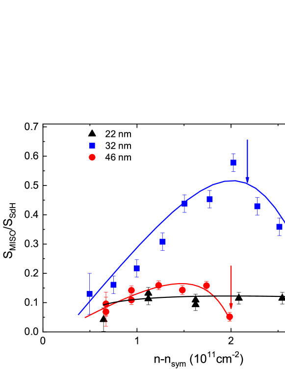
Most important in Fig. 8 in our opinion is the difference in the dependences of on . As seen the ratio for QW with nm does not depend on the density within the experimental accuracy222The first point [with cm-2], when the MISO just appears, has a large error, it corresponds to the low frequencies and it is difficult to “clear” it from the monotonic component. In wells with nm and nm, the value noticeably increases with an increase of . Such a behavior seems strange, because with an increase of electron density (i.e., with an increase of the Fermi quasimomentum) the overlapping of the wave functions of two branches located at different QW walls decreases at least in the empty spectrum [see Fig. 9(b)]. Figure 8 also shows sharp drops in at and cm-2 for structures with nm and nm, respectively. These electron densities are close to the beginning of the filling of the second subband of spatial quantization [see Table 1, Figs. 1(b) and 4(b)].
In order to understand and interpret all the results presented above, namely, the electron density dependences of the splitting magnitude, masses in the branches, MISO amplitude in the quantum wells of different widths, let us consider the predictions of the kP theory.
VI Results of calculation: the energy spectrum and wave functions
The energy spectrum for the HgTe quantum wells was calculated using the Kane’s four-band model including second order remote band contributions. The expression for the Hamiltonian of the heterostructure grown on the plane of different orientations was derived by the method described in Refs. [45, 46]. The components of the built-in strain tensor were calculated with the use of the formulas from [5]. Parameters to describe the deformation contribution to the Hamiltonian were taken from Ref. [47]. To take into account the interface inversion asymmetry we used an additional term in the Hamiltonian, which is suggested by Ivchenko [48] (see also Ref. [22] for more details).
To account for the influence of the electrons on the electric field distribution across the quantum well, the standard self-consistent procedure of simultaneous solution of the Shrödinger equation and Poisson equation
was used. Here, is the dielectric susceptibility, is the electrostatic potential, is the Fermi-Dirac distribution function, is the wave function of eight components, which has the form
| (2) |
is the density of charged donors (it is supposed that the donors are distributed uniformly across the quantum well 333It should be mentioned that the results under consideration are practically insensitive to where the donors are located – in the quantum well or in the barriers. and their density is equal to the electron density at the gate voltage for which the quantum well is symmetric ), the summation in Eq. (VI) runs over the spatial quantization subband including the “spin” index. To solve the Shrödinger equation we set the boundary conditions in the plane assuming that the center of the quantum well was located at . The value of was chosen in such a way that the wave functions at were practically equal to zero. Usually, it was enough for the value of to exceed the width of the quantum well by nm. Eq. (VI) was solved with the following boundary conditions
| (3) |
where is assumed that the gate electrode is located at positive .
To calculate the energy spectrum and wave functions for a given value, we solved simultaneously the Schrödinger and Poisson equations by using an iterative method. First, the electron spectrum is calculated for zero potential. The wave functions obtained are used to calculate the electron charge distribution corresponding to given . This distribution is substituted in right-hand side of the Poisson equation, Eq. (VI). Obtained is substituted in the Hamiltonian and then the Schrödinger equation is solved again. The procedure is repeated until the potential converges. This usually requires iterations.
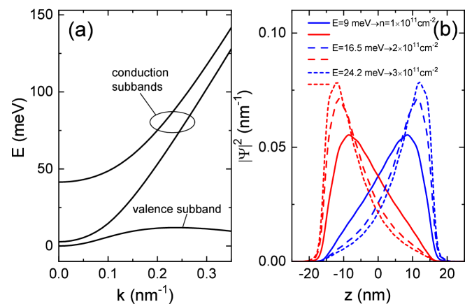
Let us first consider the calculation results for the empty spectrum, i.e., when QW is rectangular in the shape. The dispersion is depicted in Fig. 9(a), while the normalized sum of squares of eight components of wave functions for two states of the conduction band, and , for QW with nm are shown in Fig. 9(b). As seen from Fig. 9(b) the wave functions of each of the branches are localized near one of the wall, and the larger value the stronger the localization and the less the overlap of the wave functions of different branches. An approach of the empty spectrum is however inapplicable to describe the experiment. This is because the charge distribution changes and, hence, the shape of the quantum well also changes when the electron density is tuned via the voltage on the gate electrode. Self-consistent procedure should be used for that.
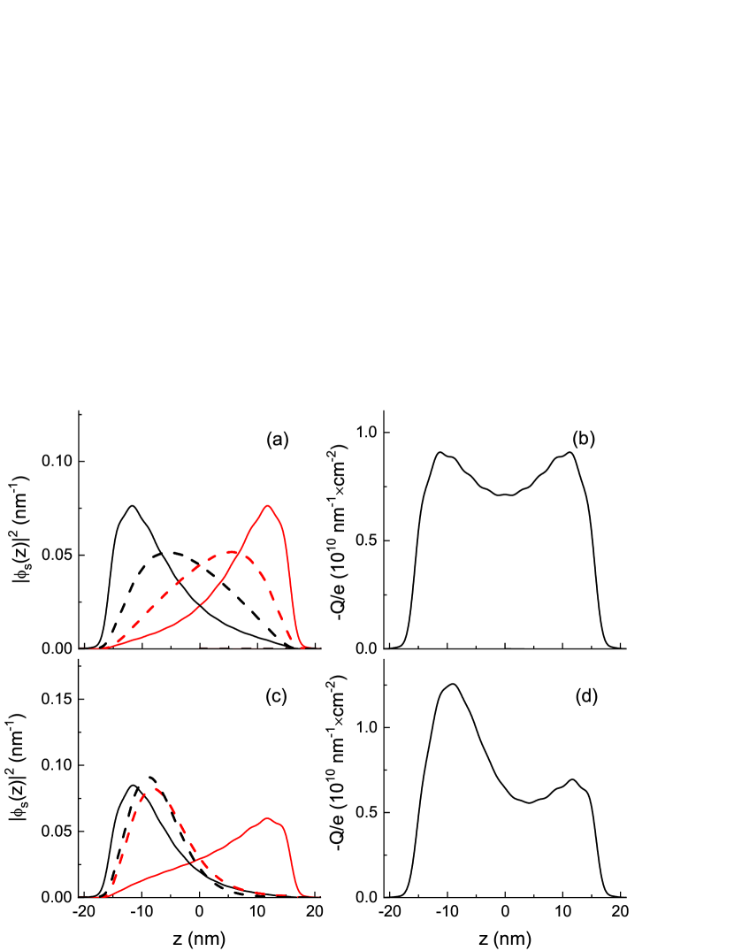
An importance of the role of the potential of electrons in the forming shape of the quantum well is illustrated by Fig. 10. The dependences for (dashed lines) and at (solid lines) for two states, , for corresponding to the electron density cm-2 before self-consistency are shown in Fig. 10(a). The distribution of electron charge is presented in Fig. 10(b). As evident from the last figure is symmetric and the average value of the electron charge position is equal to zero for this case. The same dependences after procedure of self-consistency are shown in Figs. 10(c) and 10(d). It is clearly seen that both and are modified drastically.
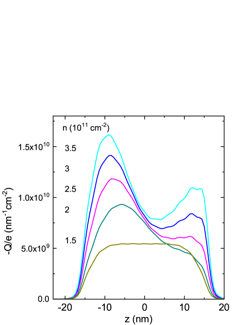
Redistribution of the electron charge in QW with the growing gate voltage inducing the electron density increase is shown in Fig. 11. As seen the charge shifts monotonically away from the gate electrode with an increase in the positive charge on it, first quickly, then slowly. The center of gravity of the charge distribution shifts away from the gate, which corresponds to the repulsion of the electronic state from the gate electrode charged positively. Such a behavior is contr-intuitive and corresponds to negative polarizability (this phenomenon for analogous structures was discussed in Ref. [50]).
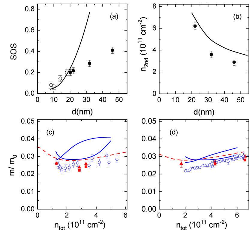
Now we in position to compare the results of self-consistent calculations with our experimental data (see Fig. 12). Let us first consider the dependence of SOS on the QW width. As seen from Fig. 12(a) both the experimental and calculated dependences grow with increasing , and for nm the theoretical dependence describes the experiment well. However, at nm, the calculated dependence increases much faster. The calculated and experimental dependences are in a rather good agreement [see Fig. 12(b)].
The comparison between the experimental and calculated effective masses is given in Fig. 12(c) and Fig. 12(d) for nm and nm, respectively. As seen the calculated effective masses are different for the split branches that qualitatively agrees with the data. However, quantitatively, this difference is much less experimentally. The other point is that the experimental masses are less as compared with the calculated ones practically for all the electron densities. Such a discrepancy for HgTe-based QWs is already discussed earlier in Ref. [2] where assumption was made that such a behavior mey result from the many-body effects.
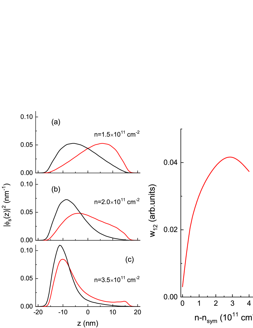
The theoretical model used provides qualitative understanding of the unusual behaviour of the MISO amplitude with growing electron density considered in Section V. As Figs. 13(a)-13(c) illustrate the growing gate voltage results to the strengthening overlap of wave functions of the branches due to their displacement away from the gate electrode that in its turn lead to strong increase of the rate of the transitions between different “spin” states [Fig. 13(d)].
The charge redistribution over direction with the varying gate voltage discussed above should manifest itself in the dependence of the capacitance between the QW and gate electrode.
VII The results of capacitance measurements
The gate voltage dependence of capacitance between 2D gas and the gate electrode results from the finite density of states of a 2D gas and it can be written as:
| (4) |
where is geometrical capacitance, is the density of states of 2D gas which is related to the effective mass of the carriers at the Fermi level as .
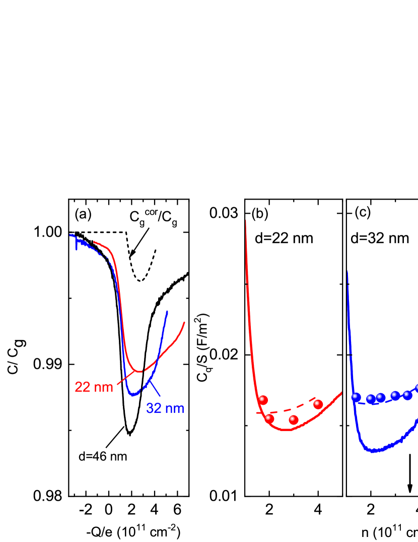
The samples under study differ slightly (by %) in dielectric thickness, gate area and value corresponding to the charge neutrality point, therefore the results of the volt-capacitance measurements obtained for different structures are shown in Fig. 14(a) as vs plot.
To determine , we used the fact that the measurements of the Hall density and SdH oscillations at different and in the “hole” region showed that (i) the degeneracy of the states of valence band top is equal to two up to the hole density cm-2; (ii) the effective mass of holes is large, its value is close to each other for all the structures and is equal to . With taking this into account the value can be obtained as , where is the experimental capacity measured within the hole region at cm-2, is the hole quantum capacity.
Figure 14(a) shows that the capacitance drops sharply cm-2 and has a minimum at the nonzero electron densities cm-2. This is due to the two factors: (i) at these QW widths, the conduction and valence bands overlap; (ii) the effective mass of holes is much (about times) larger than that of the electrons. In ordinary structures, the drop is associated with a decrease in the density of states and, therefore, with a large contribution of the quantum capacitance. The values of quantum capacity calculated from these dependences with a fixed geometric capacity are shown in Figs. 14(b)–14(d). It is seen that the value at the minimum decreases with an increase in the QW width, which seems to correspond to a smaller value of the electron mass in wider QWs. However this contradicts the experimental results on the electron masses obtained from the analysis of SdH oscillations shown in Fig. 6.
In order to understand what the seemingly smaller value of the electron mass found from can be connected with, let us consider what approximations were made when obtaining the formula, Eq. (4). It was tacitly assumed that the charge distribution in QW over axis does not change with a change in the density of charge carriers by the gate voltage. Recall that self-consistent calculations (see Fig. 10 and Fig. 11) show that changes the charge distribution in direction. In our case, as discussed above, electrons are repulsed from the gate electrode at a positive voltage that can be considered as the change (decrease in the given case) of the geometrical capacity.
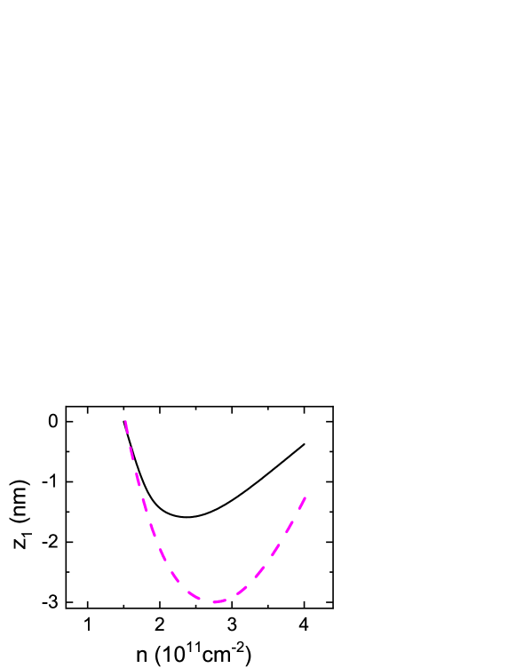
Using this simple model one can easily find how the geometrical capacity should depend on the gate voltage so that calculated from Eq. (4) with replacement of by coincides with calculated from the density of states with the use of the experimental effective mass. The results for for one of the structures is shown in Fig. 14(a) by the dashed line. As Fig. 14(a) and Fig. 14(c) illustrate the decrease of the geometrical capacity by the value of % in the minimum for structure with nm gives good agreement between values calculated from the experimental effective mass and found from the vs measurements. The simple estimate with the use of the formula of the flat capacitor gives that this decrease in the geometrical capacitance corresponds to increase of the distance between the capacitor plates, i.e., to the shift of the electron density away from the gate electrode, by the value of about nm (Fig. 15). This simple consideration agrees qualitatively with the results of theoretical calculations. This is illustrated by the same figure in which we also show the electron density dependence of the position the center of gravity of the electron charge distribution () relative to the QW center.
Thus, the redistribution of charge with the gate voltage in wide QWs is significant, and it is this redistribution that changes the dependence and results in the growing MISO amplitude with the electron density increase.
VIII Conclusion
We have experimentally studied the magnetotransport and capacitance between 2D gas and the gate electrode in HgTe-based quantum wells of nm width. The data obtained were analyzed using the well-known approach of the self-consistent calculation of the energy spectrum within the framework of the four-band kP model.
It has been shown that the splitting of the conduction band spectrum occurs due to the spin-orbit interaction, therewith, the split branches are single-spin. The splitting strength increases with the increase of the QW width. The electron effective masses in the branches at the Fermi energy are close to each other within the actual density range.
In all the structures under study, magneto-intersubband oscillations (MISO) are observed. This indicates that the overlap of the wave functions is sufficiently large. The MISO amplitude in QWs with nm increases with an increase of the total electron density. This contradicts to the expected decrease of wave function overlap with increasing calculated for the rectangular QW. To interpret such a behaviour, we applied self-consistent approach to calculate the QW energy spectrum. It has been shown that the MISO amplitude increase results from the increasing overlap of the wave functions due to their shift with the gate voltage increase which, in its turn, leads to an increase in the probability of transitions between the branches and to an increase of the MISO amplitude.
Analyzing the data we conclude that standard self-consistent calculations are only in qualitative agreement with the experimental results. A possible reason is the difference of dielectric susceptibility of think layer forming the quantum well from that of the parent bulk material as discussed in Refs. [51, 52, 34, 38]. We are not aware of papers in which this was considered for such a complicated spectrum as HgTe/Hg1-xCdxTe QWs. Further theoretical studies are needed to understand which effects are not taken into account yet in order to describe the data quantitatively.
Acknowledgements.
The research was supported by a grant of Ministry of Science and Higher Education of the Russian Federation No. 075-15-2020-797 (13.1902.21.0024).References
- Groves and Paul [1963] S. Groves and W. Paul, Band structure of gray tin, Phys. Rev. Lett. 11, 194 (1963).
- Minkov et al. [2020a] G. Minkov, V. Y. Aleshkin, O. Rut, A. Sherstobitov, A. V. Germanenko, S. Dvoretski, and N. Mikhailov, Electron mass in a hgte quantum well: Experiment versus theory, Physica E 116, 113742 (2020a).
- Gerchikov and Subashiev [1990] L. G. Gerchikov and A. Subashiev, Interface states in subbabnd structure of semiconductor quantum well, Phys. Stat. Sol. (b) 160, 443 (1990).
- Zhang et al. [2001] X. C. Zhang, A. Pfeuffer-Jeschke, K. Ortner, V. Hock, H. Buhmann, C. R. Becker, and G. Landwehr, Rashba splitting in n -type modulation-doped hgte quantum wells with an inverted band structure, Phys. Rev. B 63, 245305 (2001).
- Novik et al. [2005] E. G. Novik, A. Pfeuffer-Jeschke, T. Jungwirth, V. Latussek, C. R. Becker, G. Landwehr, H. Buhmann, and L. W. Molenkamp, Band structure of semimagnetic hg1-ymnyte quantum wells, Phys. Rev. B 72, 035321 (2005).
- Bernevig et al. [2006] B. A. Bernevig, T. L. Hughes, and S.-C. Zhang, Quantum spin hall effect and topological phase transition in hgte quantum wells, Science 314, 1757 (2006).
- Zholudev [2013] M. Zholudev, Ph.D. thesis, University Montpellier 2, France (2013).
- Ren et al. [2016] Y. Ren, Z. Qiao, and Q. Niu, Topological phases in two-dimensional materials: a review, Reports on Progress in Physics 79, 066501 (2016).
- D’yakonov and Khaetskii [1982] M. I. D’yakonov and A. Khaetskii, Zh. Eksp. Teor. Fiz. 82, 1584 (1982), [Sov. Phys. JETP 55, 917 (1982)].
- Becker et al. [2003] C. R. Becker, V. Latussek, G. Landwehr, and L. W. Molenkamp, Inverted band structure of type-iii superlattices and its temperature dependence, Phys. Rev. B 68, 035202 (2003).
- Mikhailov et al. [2006] N. N. Mikhailov, R. N. Smirnov, S. A. Dvoretsky, Y. G. Sidorov, V. A. Shvets, E. V. Spesivtsev, and S. V. Rykhlitski, Growth of hgcdte nanostructures by molecular beam epitaxy with ellipsometric control, Int. J. Nanotechnology 3, 120 (2006).
- Dvoretsky et al. [2010] S. Dvoretsky, N. Mikhailov, Y. Sidorov, V. Shvets, S.Danilov, B. Wittman, and S. Ganichev, J. of Electronic Materials 39, 918 (2010).
- Shuvaev et al. [2012] A. M. Shuvaev, G. V. Astakhov, C. Brüne, H. Buhmann, L. W. Molenkamp, and A. Pimenov, Terahertz magneto-optical spectroscopy in HgTe thin films, Semiconductor Science and Technology 27, 124004 (2012).
- Zholudev et al. [2012] M. S. Zholudev, A. V. Ikonnikov, F. Teppe, M. Orlita, K. V. Maremyanin, K. E. Spirin, V. I. Gavrilenko, W. Knap, S. A. Dvoretskiy, and N. N. Mihailov, Cyclotron resonance in hgte/cdte-based heterostructures in high magnetic fields, Nanoscale Research Letters 7, 534 (2012).
- Zoth et al. [2014] C. Zoth, P. Olbrich, P. Vierling, K.-M. Dantscher, V. V. Bel’kov, M. A. Semina, M. M. Glazov, L. E. Golub, D. A. Kozlov, Z. D. Kvon, N. N. Mikhailov, S. A. Dvoretsky, and S. D. Ganichev, Quantum oscillations of photocurrents in hgte quantum wells with dirac and parabolic dispersions, Phys. Rev. B 90, 205415 (2014).
- Dantscher et al. [2015] K.-M. Dantscher, D. A. Kozlov, P. Olbrich, C. Zoth, P. Faltermeier, M. Lindner, G. V. Budkin, S. A. Tarasenko, V. V. Bel’kov, Z. D. Kvon, N. N. Mikhailov, S. A. Dvoretsky, D. Weiss, B. Jenichen, and S. D. Ganichev, Cyclotron-resonance-assisted photocurrents in surface states of a three-dimensional topological insulator based on a strained high-mobility hgte film, Phys. Rev. B 92, 165314 (2015).
- Gusev et al. [2012] G. M. Gusev, E. B. Olshanetsky, Z. D. Kvon, A. D. Levin, N. N. Mikhailov, and S. A. Dvoretsky, Nonlocal transport near charge neutrality point in a two-dimensional electron-hole system, Phys. Rev. Lett. 108, 226804 (2012).
- Minkov et al. [2013] G. M. Minkov, A. V. Germanenko, O. E. Rut, A. A. Sherstobitov, S. A. Dvoretski, and N. N. Mikhailov, Two-dimensional semimetal in a wide hgte quantum well: Magnetotransport and energy spectrum, Phys. Rev. B 88, 155306 (2013).
- Kozlov et al. [2014] D. Kozlov, Z. Kvon, N. Mikhailov, and S. Dvoretsky, Pis’ma Zh. Eksp. Teor. Fiz. 100, 824 (2014), [JETP Letters 100, 724 (2014)].
- Minkov et al. [2014] G. M. Minkov, A. V. Germanenko, O. E. Rut, A. A. Sherstobitov, S. A. Dvoretski, and N. N. Mikhailov, Hole transport and valence-band dispersion law in a hgte quantum well with a normal energy spectrum, Phys. Rev. B 89, 165311 (2014).
- Jost et al. [2017] A. Jost, M. Bendias, J. Böttcher, E. Hankiewicz, C. Brüne, H. Buhmann, L. W. Molenkamp, J. C. Maan, U. Zeitler, N. Hussey, and S. Wiedmann, Electron–hole asymmetry of the topological surface states in strained HgTe, Proceedings of the National Academy of Sciences 114, 3381 (2017), https://www.pnas.org/content/114/13/3381.full.pdf .
- Minkov et al. [2017] G. M. Minkov, V. Y. Aleshkin, O. E. Rut, A. A. Sherstobitov, A. V. Germanenko, S. A. Dvoretski, and N. N. Mikhailov, Valence band energy spectrum of hgte quantum wells with an inverted band structure, Phys. Rev. B 96, 035310 (2017).
- Minkov et al. [2020b] G. M. Minkov, V. Y. Aleshkin, O. E. Rut, A. A. Sherstobitov, S. A. Dvoretski, N. N. Mikhailov, and A. V. Germanenko, Anisotropy of the in-plane -factor of electrons in hgte quantum wells, Phys. Rev. B 101, 085305 (2020b).
- Minkov et al. [2019] G. Minkov, V. Y. Aleshkin, O. Rut, A. Sherstobitov, A. Germanenko, S. Dvoretski, and N. Mikhailov, Spin-orbit splitting of the conduction band in hgte quantum wells: Role of different mechanisms, Physica E 110, 95 (2019).
- König et al. [2007] M. König, S. Wiedmann, C. Brüne, A. Roth, H. Buhmann, L. W. Molenkamp, X.-L. Qi, and S.-C. Zhang, Quantum spin hall insulator state in hgte quantum wells, Science 318, 766 (2007).
- Roth et al. [2009] A. Roth, C. Brüne, H. Buhmann, L. W. Molenkamp, J. Maciejko, X.-L. Qi, and S.-C. Zhang, Nonlocal transport in the quantum spin hall state, Science 325, 294 (2009).
- Gusev et al. [2011] G. M. Gusev, Z. D. Kvon, O. A. Shegai, N. N. Mikhailov, S. A. Dvoretsky, and J. C. Portal, Transport in disordered two-dimensional topological insulators, Phys. Rev. B 84, 121302 (2011).
- Minkov et al. [2015] G. M. Minkov, A. A. Sherstobitova, A. V. Germanenko, O. E. Rut, S. A. Dvoretskii, and N. N. Mikhailov, Conductance of a lateral p-n junction in two dimensional hgte structures with an inverted spectrum the role of edge states, Pisma Zh. Eksp. Teor. Fiz. 101, 522 (2015), [JETP Letters 101, 469 (2015)].
- Moore and Balents [2007] J. E. Moore and L. Balents, Topological invariants of time-reversal-invariant band structures, Phys. Rev. B 75, 121306 (2007).
- Hasan and Kane [2010] M. Z. Hasan and C. L. Kane, Colloquium : Topological insulators, Rev. Mod. Phys. 82, 3045 (2010).
- Qi and Zhang [2011] X.-L. Qi and S.-C. Zhang, Topological insulators and superconductors, Rev. Mod. Phys. 83, 1057 (2011).
- Olshanetsky et al. [2015] E. B. Olshanetsky, Z. D. Kvon, G. M. Gusev, A. D. Levin, O. E. Raichev, N. N. Mikhailov, and S. A. Dvoretsky, Persistence of a two-dimensional topological insulator state in wide hgte quantum wells, Phys. Rev. Lett. 114, 126802 (2015).
- Zhang and Zhang [2013] H. Zhang and S.-C. Zhang, Physica Status Solidi (RRL) – Rapid Research Letter 7, 72 (2013).
- Brüne et al. [2014] C. Brüne, C. Thienel, M. Stuiber, J. Böttcher, H. Buhmann, E. G. Novik, C.-X. Liu, E. M. Hankiewicz, and L. W. Molenkamp, Dirac-screening stabilized surface-state transport in a topological insulator, Phys. Rev. X 4, 041045 (2014).
- Kozlov et al. [2015] D. A. Kozlov, Z. D. Kvon, M. L. Savchenko, D. Weiss, N. N. Mikhailov, and S. A. Dvoretskii, Three-dimensional topological insulator based on a strained hgte film, Low Temperature Physics 41, 82 (2015).
- Savchenko et al. [2016] M. L. Savchenko, D. Kozlov, Z. Kvon, N. N. Mikhailov, and S. A. Dvoretskii, Pis’ma Zh. Eksp. Teor. Fiz. 104, 311 (2016), [JETP Letters 104, 302 (2016)].
- Kozlov et al. [2016] D. A. Kozlov, D. Bauer, J. Ziegler, R. Fischer, M. L. Savchenko, Z. D. Kvon, N. N. Mikhailov, S. A. Dvoretsky, and D. Weiss, Probing quantum capacitance in a 3d topological insulator, Phys. Rev. Lett. 116, 166802 (2016).
- Ziegler et al. [2020] J. Ziegler, D. A. Kozlov, N. N. Mikhailov, S. Dvoretsky, and D. Weiss, Quantum hall effect and landau levels in the three-dimensional topological insulator hgte, Phys. Rev. Research 2, 033003 (2020).
- Mamani et al. [2009] N. C. Mamani, G. M. Gusev, O. E. Raichev, T. E. Lamas, and A. K. Bakarov, Nonlinear transport and oscillating magnetoresistance in double quantum wells, Phys. Rev. B 80, 075308 (2009).
- Raichev [2010] O. E. Raichev, Magnetoresistance oscillations in two-subband electron systems: Influence of electron-phonon interaction, Phys. Rev. B 81, 195301 (2010).
- Note [1] This is of course an approximation. In the paper [24] we show that the theory predicts nonlinear dependences and at the small splitting values. However, in order to trace the change in spin-orbit splitting with the change, such a SOS parameter is suitable.
- Lifshits and Kosevich [1955] I. M. Lifshits and A. M. Kosevich, Theory of magnetic susceptibility in metals at low temperatures, Zh. Eksp. Teor. Fiz. 29, 730 (1955), [Sov. Phys. JETP 2, 636 (1956)].
- Minkov et al. [2020c] G. M. Minkov, O. E. Rut, A. A. Sherstobitov, S. A. Dvoretski, N. N. Mikhailov, V. A. Solov’ev, M. Y. Chernov, S. V. Ivanov, and A. V. Germanenko, Magneto-intersubband oscillations in two-dimensional systems with an energy spectrum split due to spin-orbit interaction, Phys. Rev. B 101, 245303 (2020c).
- Note [2] The first point [with cm-2], when the MISO just appears, has a large error, it corresponds to the low frequencies and it is difficult to “clear” it from the monotonic component.
- Los et al. [1996] J. Los, A. Fasolino, and A. Catellani, Generalization of the kp approach for strained layered semiconductor structures grown on high-index-planes, Phys. Rev. B 53, 4630 (1996).
- Becker et al. [2000] C. R. Becker, V. Latussek, A. Pfeuffer-Jeschke, G. Landwehr, and L. W. Molenkamp, Band structure and its temperature dependence for type-iii superlattices and their semimetal constituent, Phys. Rev. B 62, 10353 (2000).
- Takita et al. [1979] K. Takita, K. Onabe, and S. Tanaka, Anomalous magnetoresistance and band crossing in uniaxially compressed hgte, physica status solidi (b) 92, 297 (1979).
- Ivchenko [2005] E. Ivchenko, Optical Spectroscopy of Semiconductor Nanostructures (Alpha Science International, Harrow, UK, 2005) p. 427.
- Note [3] It should be mentioned that the results under consideration are practically insensitive to where the donors are located – in the quantum well or in the barriers.
- Aleshkin et al. [2021] V. Y. Aleshkin, A. Germanenko, G. Minkov, and A. Sherstobitov, Anomalous electron polarizability of hgte quantum wells, Physica E 128, 114606 (2021).
- Andlauer and Vogl [2009] T. Andlauer and P. Vogl, Full-band envelope-function approach for type-ii broken-gap superlattices, Phys. Rev. B 80, 035304 (2009).
- [52] J. Zhu, C. Lei, and A. H. MacDonald, Electronic properties of thin films of tensile strained hgte, arXiv:1804.01662 .