A material view on extrinsic magnetic domain wall pinning in cylindrical CoNi nanowires
Abstract
Speed and reliability of magnetic domain wall (DW) motion are key parameters that must be controlled to realize the full potential of DW-based magnetic devices for logic and memory applications. A major hindrance to this is extrinsic DW pinning at specific sites related to shape and material defects, which may be present even if the sample synthesis is well controlled. Understanding the origin of DW pinning and reducing it is especially desirable in electrochemically-deposited cylindrical magnetic nanowires (NWs), for which measurements of the fascinating physics predicted by theoretical computation have been inhibited by significant pinning. We experimentally investigate DW pinning in CoxNi100-x NWs, by applying quasistatic magnetic fields. Wire compositions were varied with , while the microstructure was changed by annealing or varying the pH of the electrolyte for deposition. We conclude that pinning due to grain boundaries is the dominant mechanism, decreasing inversely with both the spontaneous magnetization and grain size. Second-order effects include inhomogeneities in lattice strain and the residual magnetocrystalline anisotropy. Surface roughness, dislocations and impurities are not expected to play a significant role in DW pinning in these wire samples.
I Introduction
The motion of domain walls (DWs) has been a point of high interest in magnetism since the early 20th century1, as it is often involved in magnetization reversal processes. Extensive efforts have been made to comprehend the underlying physics and its link with sample shape and microstructure. One-dimensional nanosized conduits such as strips and wires are a textbook case to model and therefore understand DW motion, owing to the small number of degrees of freedom involved2, 3, 4, 5. The rise of spintronics brought prospects for a wide range of applications for DW motion in such conduits. Some prime examples include the dynamic switching of magnetic tunnel junctions or spin valves 6, the ultra fast speeds achieved in compensated ferrimagnets7 or the progress made towards realizing a non-volatile shift-register memory device8, 9, 10. Across all of these, reliability and wall velocity stand out as critical parameters governing viability. While the physics of DW motion is now rather well understood, both reliability and velocity may suffer from imperfections in material and shape, called extrinsic pinning sites11, 12, 13, 14, 15. These act as energy wells or barriers that a DW must overcome16, 17 to move, translating into a minimum driving force that must be applied to allow for wall motion past each pinning site, such as a critical depinning field, , or critical depinning current, , for the case of DW motion induced by the application of an external magnetic field or spin-transfer torque, respectively.
The detailed nature of extrinsic pinning sites is unclear even in simple one-dimensional magnetic systems. Various ideas have been put forth, including compositional changes along the sample length18, 19, 20, polycrystallinity and associated grain boundaries14, 21, surface defects and roughness11, 13, dislocations22, impurities23 or strain24, 25, which all lead to local variations in magnetic properties such as magnetocrystalline anisotropy, spontaneous magnetization, exchange stiffness, etc and therefore variations in the energy landscape felt by the DW.
Among one-dimensional magnetic conduits, there exists a specific interest in cylindrical ferromagnetic nanowires (NWs), synthesized by electrochemical deposition into porous membranes26. Indeed, theory and simulations predict fascinating novel physics in these 3D systems27, such as DW velocities in excess of with no Walker breakdown3, 28, only limited by the emission of spin waves (spin-Cherenkov effect)29, 30. We recently provided a first experimental evidence of the very high velocities15 in CoNi NWs, however, the results were affected by DW pinning, resulting in a large spread in the results. The pinning field in cylindrical NWs is typically one order of magnitude higher than in thin flat strips of the same material however deposited by physical methods31. This obstacle must be overcome in order to further study the fascinating fast motion of DWs and associated effects in these systems.
A vast quantity of reports concern the coercivity of NWs32, 33, 34, 35, 36, 37, 38, 39, 40. In most cases, especially for rather soft-magnetic materials, this relates to the nucleation of DWs from a wire end, shown to depend only on the geometry and materials parameters. For instance, coercivity in CoNi NWs shows a minimum of nucleation field for composition 39, 26. However, the nucleation field in such NWs is larger than , so that the DW runs the entirety of the wire once nucleated, and nothing is learned about extrinsic pinning through coercivity. Far fewer studies have focused on pinning. These largely theoretical and simulation-based works have considered DW pinning on diameter41, 42, 43, 44, 45 or composition modulations19, 20, 46, on surface roughness13, 41 and on regions with different magnetocrystalline anisotropy, which can be likened to a polycrystalline texture13, 47. All successfully identify that these material defects cause DW pinning, and some relate them primarily to variations in magnetostatic and anisotropy energy. However, only Ivanov and Orlov13 provide a detailed theoretical picture of DW pinning due to surface roughness and polycrystallinity. A limited number of experimental pieces of work have focussed on pinning sites fabricated on purpose, through composition20 or diameter modulations42, 43. Other possible explanations for DW pinning, such as grain boundary pinning, have not been supported experimentally.
In this paper we address the issue of DW pinning in cylindrical NWs with rather soft-magnetic properties, by evaluating experimentally the impact of various types of defects on DW pinning in CoNi NWs. We consider compositions in the range of to Co with a view to exhibit a low-pinning material, since we may expect low pinning from CoNi NWs that exhibit the lowest coercive field26, or from CoNi material that exhibits near-zero magnetocrystalline anisotropy and magnetostriction48.
II Methods
For the electrochemical deposition of NWs, templates of porous anodized aluminium oxide (AAO) membranes were synthesized as described elsewhere26 and a coating of Au was sputtered on a single side to provide an electric contact for electrodeposition. We fabricated samples with compositions CoNi, CoNi and CoNi starting from modified Watt’s electrolytes with compositions summarized in Table 1. The electrolyte pH was set to for all depositions, except once lowered to to reduce the NW grain size with respect to the standard sample49, 50, by adding NaOH or H2SO4. Depositions were carried out in a three-electrode electrochemical cell at vs. an Ag/AgCl/NaCl () reference electrode. After NW growth, the gold contact was etched in a KI/I2 solution. Annealing of some batched was carried out to allow for grain growth and crystallographic relaxations51, 52, 53, by placing filled membranes into a tubular vacuum oven at for .
| CoNi | CoNi | CoNi | ||||
|---|---|---|---|---|---|---|
| Compound | (mol) | (g) | (mol) | (g) | (mol) | (g) |
| CoSO7H2O | 0.0182 | 0.5104 | 0.0282 | 0.7930 | 0.0450 | 1.2649 |
| CoCl6H2O | 0.0012 | 0.0276 | 0.0018 | 0.0428 | 0.0027 | 0.0649 |
| NiSO6H2O | 0.3120 | 8.2005 | 0.2934 | 7.7109 | 0.2375 | 6.2426 |
| NiCl6H2O | 0.0551 | 1.3087 | 0.0518 | 1.2306 | 0.0400 | 0.9508 |
| H3BO3 | 0.5000 | 3.0915 | 0.5000 | 3.0915 | 0.5000 | 3.0915 |
| saccharin | 0.0150 | 0.2750 | 0.0150 | 0.2750 | 0.0150 | 0.2750 |
NW compositions were checked by atomic absorption spectroscopy (AAS) and by scanning electron microscopy energy-dispersive x-ray (SEM EDX) analysis. Vibrating sample magnetometry (VSM) and x-ray diffraction (XRD) were carried out on large () pieces of filled AAO membrane. For XRD, diffractograms were obtained with a symmetric geometry and a Copper filament as x-ray source, with characteristic radiation with a wavelength of . Individual diffraction peaks in a diffractogram were fitted using a Gaussian to extract both peak position and peak width.
Unless stated otherwise, NWs were freed by dissolving the AAO membrane in chromic and orthophosphoric acid solution at for hours. The NW-acid solutions were rinsed several times in distilled water and finally in ethanol to produce clean NW suspensions. Drops of suspension were then dispersed onto silicon wafers with prepared gold alignment marks and NWs were located using SEM. These marks allowed to seek the wires were in the optical view of the magnetic force microscope (MFM), which was used to monitor DW motion. Individual NW samples were also imaged with transmission electron microscopy (TEM), by dispersing NWs on a specific lacey-carbon grid.
III Results
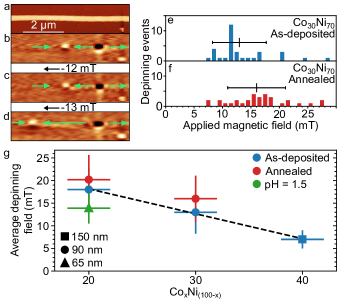
DW depinning was measured by imaging DW positions with MFM before and after applying an external magnetic field oriented along the NW long axis, with pulse duration of about . By slowly increasing the amplitude of the applied field between each measurement, the field required to depin DWs from specific pinning sites could be determined. Fig. 1a shows an atomic force microscopy (AFM) image of a section of an individual, as-deposited -diameter CoNi NW. The corresponding MFM image in Fig. 1b shows the initial magnetic configuration with two DWs located along the wire length, and the direction of magnetization within the three longitudinal domains indicated by green arrows. The MFM image in Fig. 1c shows the magnetic configuration after applying a magnetic field pulse with amplitude , remaining unchanged. Imaging after applying a field pulse (Fig. 1d) shows that the left-hand wall was depinned and moved to a different, presumably stronger pinning site, hence the depinning field of the initial site is in the range . Such measurement series were repeated on multiple NWs for each sample type in order to determine a distribution of depinning field amplitudes.
Fig. 1e,f shows distribution of depinning field for both as-deposited and annealed CoNi NWs, respectively. Note that the procedure of applying quasistatic pulses of field with rising values during a series implies that for any given wire contributing to the statistics in these figures, once the first depinning event has occured we cannot measure events associated with lower pinning fields. Thus, these distributions probably over-emphasize pinning sites associated with a high value of field, partly contributing to their large width. Still, the average and standard deviation of the distributions are plotted as horizontal lines, illustrating a lower average depinning field of the as-deposited sample. The variation of average depinning field as a function of cobalt content and different preparation methods is presented in Fig. 1g, with different NW diameters indicated by marker shapes. In the case of the as-deposited NW samples (blue), the average depinning field decreases from to to as the Co content increases from to to . This nearly linear decrease is indicated by the dashed guide to the eye. NWs deposited from an electrolyte with a pH of (Fig. 1g, green) exhibit a lower average depinning field compared to the NWs deposited from a normal electrolyte with a pH of (blue). Conversely, NWs that were annealed in the AAO membrane at for (Fig. 1g, red) display a larger average depinning field (data from Fig. 1f).
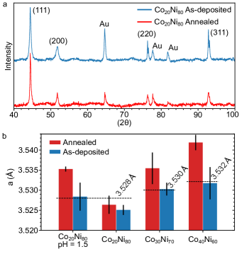
It is evident from Fig. 1g that NW samples prepared by different methods lead to variations in average depinning fields. To tentatively separate the effects of composition and microstructure between the samples, we used XRD to analyze the various NWs while in the AAO membranes. The XRD diffractogram of as-deposited CoNi NWs is shown in blue in Fig. 2a. The peaks at , , , are consistent with reflections from the (111), (200), (220), and (311) planes of face-centered cubic CoNi alloy, while the peaks at , and are consistent with diffraction from gold, suggesting that the etching of the bottom electrode is incomplete. The absence of any other peak indicates the single phase of the electrodeposited NWs.
After subtraction of the calibrated instrumental offset, the diffraction peak angles were used to calculate the lattice coefficient, , of the sample’s cubic unit cell, according to Bragg’s law, giving an average (Fig. 2b). This is slightly below the expected value of the lattice coefficient for CoNi, , calculated using Vegard’s law, indicating a general compression of the unit cell with respect to the equilibrium state, at least along the wire axis. Annealing of the CoNi NWs sample does not change the XRD pattern (Fig. 2a, red) qualitatively, however, a similar calculation of the lattice coefficient gives and thus possibly an increase in unit cell size although affected by the error bar. At this stage we need to discuss the impact of the AAO membrane. Heating of the AAO and its concomitant thermal expansion leads to a reduction of the pore diameter. This and the NW’s own thermal expansion cause a radial stress of the wire which would tend to cause an expansion along the wire axis. This is reversed upon cooling, however, the original shape may not be entirely recovered, leaving a difference with the non-annealed sample. Further, as the sample is quickly removed from the oven, the rapid cooling that occurs could be linked to quenching and partly freeze the expanded high-temperature structure22. Fig. 2b shows the lattice coefficients calculated from XRD peak positions of all samples, with the dashed lines indicating for the given composition52. For both the as-deposited (blue) and the annealed samples (red), increases with increasing Co content, as a result of the added volume of the larger Co atoms, in agreement with the increasing . All as-deposited samples, except the previously discussed CoNi, have a near perfect match between and , and it thus follows that the crystallites within the electrodeposited material are essentially strain-free. Furthermore, annealing leads to an increase in , however, unlike the previously discussed case of annealed CoNi, the other three instances of annealing (CoNi with pH , CoNi and CoNi) lead to , indicative of crystal lattices under slight tensile stress along the NW axis. Finally, CoNi NWs electrodeposited from an electrolyte with a pH of exhibit a larger lattice coefficient that is closer to than standard growth CoNi NWs. This may be a result of the significantly slower deposition rate, allowing atoms to rearrange and grow overall less strained crystals.
Further microstructural information can be obtained using the Williamson-Hall approach54, 55, to separate the effects of distribution of inhomogeneous crystal strain, , and grain size, , on peak broadening, , of the XRD diffractogram. This method is more suitable than relying on the more basic Scherrer formula, which can underestimate the grain size, affected by and instrumental resolution. Indeed, both and contribute to the finite width of peaks, the first by a spread of each diffraction peak and depending on the angle, , the second through a fixed peak width increase scaling as (Scherrer formula). In other words, the effect of increases at large , whereas the effect of remains constant. Therefore, after correcting for instrumental peak broadening in the XRD diffractogram, the impact of and can be separately identified by following , with the x-ray wavelength and a shape factor best approximated as . A Williamson-Hall plot for as-deposited CoNi with pH NWs is shown in Fig. 3a. From the above equation, the slope () and y-intercept () of the blue linear regression of the data set provide the amplitude of strain distribution and grain size, respectively. The error for this information is given by the maximum and minimum possible slopes, as shown by dashed lines, however, with the minimum slope not below zero since is unphysical. The full Williamson-Hall plot for both as-deposited and annealed NWs is given in Fig. 3b, showing the linear regression fits of as-deposited and annealed samples as solid and dashed lines, respectively. For the as-deposited CoNi and CoNi NW data the regression slope should be negative from the numerical fit, however bounded to the zero slope as constraint for its physical meaning, as mentioned above.
Fig. 3c shows the grain size for both as-deposited (full bar) and annealed (open bar) NWs calculated from the Williamson-Hall plot. The error bars are calculated by the same method using the maximum and minimum possible fitted lines, however, note that the error bars for annealed CoNi with pH and CoNi extend to , which exceeds the instrumental limit for peak widths below in and thus . Grain sizes calculated using the Scherrer formula, , again with the shape factor , should provide a lower bound for grain size, as discussed previously. These are indicated by grey crosses, which match indeed well with the lower bound of the error bars. The grain size of standard as-deposited NWs is , with little change in composition. However, it must be noted that the large data spread and uncertainties in the Williamson-Hall plot may affect the accuracy of these calculated values. Decreasing the electrolyte pH reduces the grain size to (CoNi with pH ), possibly resulting from the increased hydrogen evolution at the cathode. This inhibits grain growth by limiting surface diffusion of adatoms and instead favours grain nucleation56. Conversly, annealing increases the grain size to nd for CoNi, CoNi with pH and CoNi, respectively, due to the recrystallization and growth initiated by the heat treatment51, 52, 53.
Similarly, the distribution of inhomogeneous crystal strain was calculated from the slope as . Where the linear regression slope was positive, the strain distribution was calculated as 0.00067 (annealed CoNi), 0.00074 (CoNi with pH ), 0.00117 (annealed CoNi with pH ) and 0.00188 (annealed CoNi), however, for all measurements the error bar extends to nearly one order of magnitude larger values. Considering the large error associated with these results, it is not possible to draw definite conclusions about the strain distribution in these NW samples.
The grain sizes and strain distributions that we measure are very similar to values for nanocrystalline nickel thin film, also electrodeposited from a Watt’s or purely sulphate electrolyte. A large number of studies made use of the Scherrer formula and found grain sizes of the order of to , for deposition conditions close to the ones used in this work 57, 58, 59, 60, 61. Fewer studies have investigated electrodeposited NiCo alloys 52, 62, but the reported grain sizes largely match those of pure Ni. In particular, Tóth et al. 52 investigated the effect of annealing at for on the grain size of nanocrystalline CoNi alloys and found an increase from to for low Co contents. The experiment that is most similar to the present study was performed by Dost et al. 63, where annealing of -diameter Ni nanowires at for increased the grain size from to . TEM imaging also revealed that after annealing grains often occupied the entire diameter of the wire. The grain sizes of our as-deposited materials match well with values from literature, however, a direct comparison of the impact of annealing in this study and previous literature cannot be made, because the starting material and annealing recipes differ. Regarding the grain size of deposits made with a lower electrolyte pH, there are no reports on nanocrystalline CoNi and other studies investigate pH . Still, in the CoFe alloys studied by Riemer et al. 56, a to grain size reduction was reported when changing the pH from to and in the NiCu alloys studied by Alper et al. 50 a to grain size reduction was reported when changing the pH from to . Strain distribution is considered less often than grain size, especially since most studies discuss only the Scherrer formula to analyse XRD peak broadening. The studies that do report on strain distribution in nanocrystalline Ni films find 53, 61 and Wang et al. 53 note that this reduces by by annealing at for .

IV Discussion of the origin of pinning
DW pinning should not occur in a homogeneous singlecrystalline NW with a perfect cylindrical shape. However, such a wire is unachievable in practice, and any deviation from perfection should lead to DW pinning. This includes diameter modulation and surface roughness, polycrystallinity and the associated grain boundaries, strain, changes in composition, line and point defects such as dislocations and impurities. Based on the results presented in the previous section, we evaluate below the phenomena most likely responsible for DW pinning, grouping them in three categories: i) surface roughness and other shape defects; ii) polycrystallinity and its interplay with magnetocrystalline anisotropy and inverse magnetostriction; iii) material defects such as inhomogeneities, grain boundaries, dislocations, impurities. General aspects applying to those different situations are described first, in the paragraph below.
General considerations
To set orders of magnitude, the models discussed are applied to a wall of length , a reasonable scaling law for the wire diameters considered here, in the range a few tens to a hundred of nanometers64. We will also use the textbook model of Becker-Kondorski16, 65 for domain-wall pinning in a one-dimensional framework, relating the depinning field to the energy landscape :
| (1) |
with the cross-sectional area of the one-dimensional conduit, in the present situation, and the position-dependent net energy of the DW, labeled in Joules.
Surface roughness
Here we evaluate to which extent deviations from perfect translational symmetry in the shape of a nanowire may explain the pinning of DWs in our systems. Deviation from the perfect cylindrical shape may take the form of local modulations of diameter (i.e., correlated around the wire diameter), or general roughness. Analytical modeling cannot cover the general case of pinning on such defects, and approximations must be made. To provide some generality and therefore robustness in the discussion and comparison with experiments, we consider three models of a very different kind.
A first model may be adapted from Bruno et al., evaluating the contribution of dipolar energy to magnetic anisotropy in thin films, related to the existence of roughness66. This model predicts a cost for planar anisotropy amounting to a net energy, written
| (2) |
is the surface area of the thin film considered, the average deviation for the roughness, the correlation length. with an infinite negative slope, sharply decreasing to and . Assuming , one may neglect long-range correlations on magnetostatic energy, and therefore model the surface of a cylindrical wire with the rolled surface of a thin film. We combine Eq.(1) to Eq.(2) with , considering a distance equal to the roughness correlation length, and averaging azimuthally over a number of correlation areas , we obtain a formula for the depinning field:
| (3) |
A second model, proposed by Ivanov and Orlov, considers specifically the cylindrical geometry, with an azimuthally correlated roughness13. The models predicts that
| (4) |
Here we disregard the square root as , and pertains to the statistical distribution of strength of pinning sites on a long length scale , an aspect not considered in the other two models. is the volume of defects at the scale of a DW, and . We finally have:
| (5) |
Yet a third model, developed by de Riz, intends to describe gentle and controlled variations of diameter. The propagation field is close to . However, this model is valid for modulations larger than the wall width, which is opposite to the situation of roughness, so that we cannot simply consider that . Instead, as a rule of thumb we may renormalize the impact of the modulation of diameter with the length of the full DW, i.e., with an extra coefficient . This leads to:
| (6) |
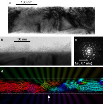
Interestingly, although all three models have a very different fundamental basis and a priori range of application, they all lead to pinning scaling with , simply with a different coefficient, and statistical azimuthal averaging for Bruno’s model. This expectation is opposite to our experimental observation that the pinning field decreases with increasing (Fig. 1). This suggests that roughness coupled with dipolar effect is not the leading mechanism of pinning in our case. This is consistent with the fact that wires electrochemically deposited in AAO templates are known to be very smooth, resulting from the amorphous structure of the aluminium oxide, unless modulations of diameter may result from instabilities during the anodisation step 67. TEM imaging of nanowires similar to those studied here revealed that beyond a possible native oxide layer, no noticeable surface roughness could be observed (Fig. 4a,b). Further, imaging with TEM holography (Fig. 4d) showed that a domain wall was pinned along the low roughness wire segment shown already in 4a. Such low impact from pinning due to surface roughness may not be the case for polycarbonate templates, which display a roughness intrinsically linked with the molecular size of the underlying polymers 68, 69.
Polycrystallinity
Polycrystallinity leads to spatial variations of magnetocrystalline or magnetoelastic anisotropy energy density , due to different grain orientations. This converts into a position-dependent energy of a DW, which implies pinning. In magnetically-soft bulk-like systems, this situation can be described with the Herzer model14, 70, averaging the anisotropy energy over the large number of grains inside a DW. The width of the latter is found self-consistently to scale with . This model is not suitable for cylindrical nanowires, for which is largely determined by magnetostatics and possibly exchange, scaling approximately with in our situation. Instead, we may consider the change of energy of a DW upon motion with distance , and apply the Becker-Kondorski model [Eq.(1)]. , with the change of number of grains in the DW upon motion. This leads to:
| (7) |
Let us apply Eq.(7) to our material with largest magnetocrystalline and magnetoelastic anisotropy, CoNi. At room temperature, the cubic coefficient for magnetocrystalline anisotropy is 71. The magnetoelastic coupling coefficients and are in the range of 48. Considering strain (Fig. 2) in the as-grown material, the resulting anisotropy density is . Eq.(7) applied with , , and the above values for density of anisotropy energy leads to pinning fields or below. This is an order of magnitude lower than experimental values. Besides, those two sources of anisotropy are expected to vanish almost simultaneously for a composition around CoNi, while in our wires the pinning field is the highest. Thus, experimental observations are inconsistent with polycrystallinity combined with magnetocrystalline or magnetoelastic anisotropy energy as the source of DW pinning in our nanowires.
Material defects
A potential imperfection in the material are inhomogeneities in composition of the CoNi alloy, leading to an axial gradient of magnetic energy for a DW. While this may be done on purpose20 to engineer DW positions, undesired inhomogeneities may also arise from potential instabilities or limitations of diffusion during electroplating. However, SEM EDX line scans evidenced homogeneous compositions along the wire lengths in all of our studied samples.
A usual defect in materials is dislocations. Yu et al. 72 noticed that coercive fields increase for larger dislocation densities. Lindquist et al. 21 directly observed pinning on dislocations in bulk magnetite, in which higher dislocation densities and longer dislocation lengths increase depinning fields, while pinning is decreased for larger magnetization. This hints at an inhomogeneity of magnetoelastic anisotropy due to strain around the dislocation, balanced by the pressure induced on the DW by the Zeeman energy. The lowering of the micromagnetic energy around a dislocation has been modeled, promoting nucleation for magnetization reversal73. The increase of and the experimental decrease of pinning for larger Co content are consistent, however again we would expect very low pinning for the CoNi alloy with vanishing magnetostriction. Besides, it is known that annealing reduces dislocation lengths and densities51, 52, 53 and thus pinning, while we observe an increase of pinning upon annealing (Fig. 1e-f). Therefore, dislocations are probably not the most active source of pinning in our case.
Another kind of material defect is grain boundaries. These are by nature two-dimensional, potentially having a larger impact than dislocation on pinning DW, which are two-dimensional as well. The pinning of DW on grain boundaries could indeed be observed directly, e.g. with Lorentz TEM in bulk FeCo alloys22, 72. The reason for pinning at a grain boundary is the various disruptions in the material, such as mismatch of crystalline lattices, strain and possibly accumulation of impurities, including non-magnetic. Accordingly, micromagnetic material parameters may be inhomogeneous, including magnetization, anisotropy and exchange stiffness. A one-dimensional model of DW shall reasonably well describe such situations. This has been the focus of many reports for the search of explanations of coercivity in practical materials, and tackling the Brown paradox74. Aharoni considered a step75 or a linear decrease76 in magnetic anisotropy. This can be generalized to a step77 or the local variation78 of any micromagnetic parameter. In all cases the propagation field scales inversely with magnetization, as the result of the balance of the Zeeman pressure against a magnetization-independent energy profile. This is a general feature in the physics of coercivity, valid also in other situations such as elastic domain walls bending between pinning sites79, 80. The only exception is pinning originating from dipolar anisotropy on roughness, as examined in the first case above, whose energy depends on magnetization and scale with .
Coming back to our measurements, pinning on grain boundaries is consistent with the decrease in depinning field [ to to ] with increasing Co content and increasing in the as-deposited NW samples (Fig. 1), which all share similar grain sizes (Fig. 3). Besides, this explanation is compatible with a pinning persisting for the CoNi alloy despite its vanishing microscopic sources of anisotropy, unlike the hypothesis of the effect of polycrystallinity examined previously. Still, if the grain boundary area is smaller than the section of the wire, the pinning effect is probably averaged out over multiple grain boundaries. Again, this fact is consistent with the increase of pinning strength upon annealing (Fig. 3). Not only grain boundaries are expected to become more extended, but annealing also promotes impurity diffusion to the grain boundaries81. The reduced depinning field for NWs deposited with [] matches with the reduced grain size compared to the as-deposited NWs []. Similarly, one may expects pinning to decrease with increasing NW diameter, related to the averaging of energy over the number of grains boundaries across the diameter.
Overview and discussion
To conclude the above analysis of various physical reasons for pinning, the most plausible explanation lies in the role of grain boundaries, able to affect micromagnetic material parameters locally. Surface roughness and random anisotropy in a polycrystalline material probably play a minor role in the present case. Still, the granular structure of the material has an impact, partially averaging the effect for smaller grain size, and thereby decreasing the pinning effect. It is possible to reduce the depinning field by increasing , here through a larger Co content, however, the appearance of the hexagonal close packed Co phase above a composition of CoNi37 may increase pinning due to the increasing magnetocrystalline anisotropy. However, this trend may not apply for current-driven DW motion, for which a higher transfer of angular momentum is required for large magnetization. Initial experiments comparing as-deposited and annealed diameter CoNi NWs revealed an increase in depinning current from in as-deposited wires to in annealed wires, which matches the trend observed under quasistatic fields. However, it appears that the changes in pinning strength have a much greater impact on than on . Finally, although reducing the grain size appears to be an effective method to reducing pinning strength, it also leads to increased resistance in NWs. Therefore, temperature-assisted depinning shall crucially be taken account in the analysis of experiments, and would also imply a higher power consumption in applications.
V Conclusion
We have experimentally investigated DW pinning at room temperature in electrodeposited and rather magnetically-soft CoNi NWs, with , and . Pinning is highest for and decreases linearly with increasing Co content, scaling roughly with . This observation is not compatible with pinning governed by surface roughness, which should rather increase in proportion to . Also, this does not support the role of magnetocrystalline anisotropy and magnetostriction, as at room temperature these are lowest nearly simultaneously for the CoNi concentration. This suggests that pinning is governed by microstructural defects such as grain boundaries, supported by information on grain size and boundaries brought by XRD and TEM, and the increase of pinning for larger grain size . This suggests a handle to controlling DW pinning in electrodeposited wire by decreasing through engineering of deposition parameters or conversely increasing by annealing.
VI Acknowledgements
M. S. acknowledges a grant from the Laboratoire d’excellence LANEF in Grenoble (ANR-10-LABX-51-01). The authors acknowledge financial support from the CNRS-CEA “METSA” French network (FR CNRS 3507).
References
- Sixtus and Tonks 1931 K. J. Sixtus and L. Tonks, Phys. Rev. 37, 930 (1931).
- Beach et al. 2005 G. S. D. Beach, C. Nistor, C. Knuston, M. Tsoi, and J. L. Erskine, Nat. Mater. 4, 741 (2005).
- Thiaville and Nakatani 2006 A. Thiaville and Y. Nakatani, “Spin dynamics in confined magnetic structures III,” (Springer, Berlin, 2006) Chap. Domain-wall dynamics in nanowires and nanostrips, pp. 161–205.
- Mougin et al. 2007 A. Mougin, M. C. andJ.P. Adam, P. Metaxas, and J. Ferré, Europhys. Lett. 78, 57007 (2007).
- Boulle et al. 2011 O. Boulle, G. Malinowski, and M. Kläui, Mater. Sc. Eng. R: Rep. 72, 159 (2011).
- Grimaldi et al. 2020 E. Grimaldi, V. Krizakova, G. Sala, F. Yasin, S. Couet, G. S. Kar, K. Garello, and P. Gambardella, Nat. Nanotechnol. 15, 111 (2020).
- Caretta et al. 2018 L. Caretta, M. Mann, F. Büttner, K. Ueda, B. Pfau, C. M. Günther, P. Hessing, A. Churikova, C. Klose, M. Schneider, D. Engel, C. Marcus, D. Bono, K. Bagschik, S. Eisebitt, and G. S. D. Beach, Nat. Nanotechnol. 13, 1154 (2018).
- Parkin 2004 S. S. P. Parkin, “U.s. patents 6834005, 6898132, 6920062,” (2004).
- Parkin et al. 2008 S. S. P. Parkin, M. Hayashi, and L. Thomas, Science 320, 190 (2008).
- Fert et al. 2017 A. Fert, N. Reyren, and V. Cros, Nature Reviews Materials 2, 17031 (2017).
- Klaui et al. 2005 M. Klaui, H. Ehrke, U. Rüdiger, T. Kasama, R. E. Dunin-Borkowski, D. Backes, L. J. Heyderman, C. A. F. Vaz, J. A. C. Bland, G. Faini, E. Cambril, and W. Wernsdorfer, Appl. Phys. Lett. 87, 102509 (2005).
- Bogart et al. 2009 L. K. Bogart, D. Atkinson, K. O’Shea, D. McGrouther, and S. McVitie, Phys. Rev. B 79, 054414 (2009).
- Ivanov and Orlov 2011 A. A. Ivanov and V. A. Orlov, Phys. Sol. State 53, 2441 (2011).
- Herzer 1990 G. Herzer, IEEE Trans. Magn. 26, 1397 (1990).
- Schöbitz et al. 2019 M. Schöbitz, A. De Riz, S. Martin, S. Bochmann, C. Thirion, J. Vogel, M. Foerster, L. Aballe, T. O. Menteş, A. Locatelli, F. Genuzio, S. Le Denmat, L. Cagnon, J. Toussaint, D. Gusakova, J. Bachmann, and O. Fruchart, Phys. Rev. Lett. 123, 217201 (2019).
- Kondorski 1937 E. Kondorski, Phys. Z. Sowjetunion 11, 597 (1937).
- Kondorski 1940 E. J. Kondorski, J. Exp. Theor. Fiz. 10, 420 (1940).
- Vogel et al. 2011 A. Vogel, S. Wintz, T. Gerhardt, L. Bocklage, T. Strache, M.-Y. Im, P. Fischer, J. Fassbender, J. McCord, and G. Meier, Appl. Phys. Lett. 98, 202501 (2011).
- Ivanov et al. 2016 Y. P. Ivanov, A. Chuvilin, S. Lopatin, and J. Kosel, Am. Chem. Soc. Nano 10, 5326 (2016).
- Mohammed et al. 2016 H. Mohammed, E. V. Vidal, Y. P. Ivanov, and J. Kosel, IEEE Transactions on Magnetics 52, 1 (2016).
- Lindquist et al. 2015 A. K. Lindquist, J. M. Feinberg, R. J. Harrison, J. C. Loudon, , and A. J. Newell, J. Geophys. Res. 120, 1415 (2015).
- Yu et al. 1999 R. H. Yu, S. Basu, Y. Zhang, A. Parvizi-Majidi, and J. Q. Xiao, J. Appl. Phys. 85, 6655 (1999).
- Ferreira et al. 2013 V. A. Ferreira, D. Toscano, S. A. Leonel, P. Z. Coura, R. A. Dias, and F. Sato, J. Appl. Phys. 144, 013907 (2013).
- Dean et al. 2011 J. Dean, M. T. Bryan, T. Schrefl, and D. A. Allwood, J. Appl. Phys. 109, 023915 (2011).
- Lei et al. 2013 N. Lei, T. Devolder, G. Agnus, P. Aubert, L. Daniel, J.-V. Kim, W. Zhao, T. Trypiniotis, R. P. Cowburn, C. Chappert, D. Ravelosona, and P. Lecoeur, Nat. Commun. 4, 1378 (2013).
- Bochmann et al. 2017 S. Bochmann, A. Fernandez-Pacheco, M. Mačkovic̀, A. Neff, K. R. Siefermann, E. Spiecker, R. P. Cowburn, and J. Bachmann, RCS Adv. 7, 37627 (2017).
- Fernandez-Pacheco et al. 2017 A. Fernandez-Pacheco, R. Streubel, O. Fruchart, R. Hertel, P. Fischer, and R. P. Cowburn, Nat. Commun. 8, 15756 (2017).
- Wieser et al. 2010 R. Wieser, E. Y. Vedmedenko, P. Weinberger, and R. Wiesendanger, Phys. Rev. B 82, 144430 (2010).
- Yan et al. 2011 M. Yan, C. Andreas, A. Kakay, F. Garcia-Sanchez, and R. Hertel, Appl. Phys. Lett. 99, 122505 (2011).
- Hertel 2016 R. Hertel, J. Phys.: Condens. Matter 28, 483002 (2016).
- Hayashi et al. 2006 M. Hayashi, L. Thomas, Y. B. Bazaliy, C. Rettner, R. Moriya, X. Jiang, and S. S. P. Parkin, Phys. Rev. Lett. 96, 197207 (2006).
- Sellmyer et al. 2001 D. J. Sellmyer, M. Zheng, and R. Skomski, J. Phys.: Condens. Matter 13 (2001), 10.1088/0953-8984/13/25/201.
- Nielsch et al. 2002 K. Nielsch, R. Hertel, R. B. Wehrspohn, J. Barthel, J. Kirschner, U. Gösele, S. F. Fischer, and H. Kronmüller, IEEE Trans. Magn. 38, 2571 (2002).
- Hertel and Kirschner 2004 R. Hertel and J. Kirschner, Physica B 343, 206 (2004).
- Qin et al. 2005 J. Qin, J. Nogués, M. Mikhaylova, A. Roig, J. S. M. oz, and M. Muhammed, Chem. Mater. 17, 1829 (2005).
- Pitzschel et al. 2011 K. Pitzschel, J. Bachmann, S. Martens, J. M. Montero-Moreno, J. Kimling, G. Meier, J. Escrig, K. Nielsch, and D. Görlitz, J. Appl. Phys. 109, 033907 (2011).
- Vivas et al. 2012 L. G. Vivas, M. Vazquez, J. Escrig, S. Allende, D. Altbir, D. C. Leitao, and J. P. Araujo, Phys. Rev. B 85 (2012), 10.1103/physrevb.85.035439.
- Ivanov et al. 2013 Y. P. Ivanov, M. Vázquez, and O. Chubykalo-Fesenko, J. Phys. D: Appl. Phys. 46, 485001 (2013).
- Pereira et al. 2013 A. Pereira, C. Gallardo, A. P. Espejo, J. Briones, L. G. Vivas, M. Vázquez, J. C. Denardin, and J. Escrig, Journal of Nanoparticle Research 15 (2013), 10.1007/s11051-013-2041-3.
- Bochmann et al. 2018 S. Bochmann, D. Döhler, B. Trapp, M. Staňo, A. Wartelle, O. Fruchart, and J. Bachmann, J. Appl. Phys. 124, 163907 (2018).
- Dolocan 2014 V. O. Dolocan, Appl. Phys. Lett. 105, 162401 (2014).
- Berganza et al. 2016 E. Berganza, C. Bran, M. Vazquez, and A. Asenjo, Sci. Rep. 6, 29702 (2016).
- Nasirpouri et al. 2019 F. Nasirpouri, S.-M. Peighambari-Sattari, C. B. E. M. Palmero, E. B. Eguiarte, M. Vazquez, A. Patsopoulos, and D. Kechrakos, Sci. Rep. 9, 1 (2019).
- Fernandez-Roldan et al. 2019 J. A. Fernandez-Roldan, A. D. Riz, B. Trapp, C. Thirion, J. C. Toussaint, O. Fruchart, and D. Gusakova, Sci. Rep. 9, 5130 (2019), http://arxiv.org/abs/1807.06253v1 .
- Riz et al. 2020 A. D. Riz, B. Trapp, J. Fernandez-Roldan, C. Thirion, J.-C. Toussaint, O. Fruchart, and D. Gusakova, in Magnetic Nano- and Microwires (Elsevier, 2020) pp. 427–453.
- Bran et al. 2018 C. Bran, E. Berganza, J. A. Fernandez-Roldan, E. M. Palmero, J. Meier, E. Calle, M. Jaafar, M. Foerster, L. Aballe, A. F. Rodriguez, R. P. del Real, A. Asenjo, O. Chubykalo-Fesenko, and M. Vazquez, Am. Chem. Soc. Nano 12, 5932 (2018).
- Franchin et al. 2011 M. Franchin, A. Knittel, M. Albert, D. Chernyshenko, T. Fischbacher, A. Prabhakar, and H. Fangohr, Phys. Rev. B 84, 094409 (2011).
- Kadowaki and Takahashi 1981 S. Kadowaki and M. Takahashi, J. Phys. Soc. Jap. 50, 1154 (1981).
- Natter and Hempelmann 1996 H. Natter and R. Hempelmann, jpchem 100, 19525 (1996).
- Alper et al. 2008 M. Alper, H. Kockar, M. Safak, and M. C. Baykul, J. Alloys. Compd. 453, 15 (2008).
- Qin et al. 2002 D. Qin, C. Wang, Q. Sun, and H. Li, Appl. Phys. A 74, 761 (2002).
- Tóth et al. 2010 B. G. Tóth, L. Péter, A. Révész, J. Pádár, and I. Bakonyi, Eur. Phys. J. B 75, 167 (2010).
- Wang et al. 2004 Y. M. Wang, S. Cheng, Q. M. Wei, E. Ma, T. G. Nieh, and A. Hamza, Scripta Mater. 51, 1023 (2004).
- Williamson and Hall 1953 G. K. Williamson and W. H. Hall, Acta Metall. Mater. 1, 22 (1953).
- Mote et al. 2012 V. D. Mote, Y. Purushotham, and B. N. Dole, J. Theor. Appl. Phys. 6, 2 (2012).
- Riemer et al. 2009 S. Riemer, J. Gong, M. Sun, and I. Tabakovic, J. Electrochem. Soc. 156, D439 (2009).
- Rashidi and Amadeh 2008 A. M. Rashidi and A. Amadeh, Surface and Coatings Technology 202, 3772 (2008).
- Rashidi and Amadeh 2009 A. M. Rashidi and A. Amadeh, Surface and Coatings Technology 204, 353 (2009).
- Ebrahimi et al. 1999 F. Ebrahimi, G. R. Bourne, M. S. Kelly, and T. E. Matthews, Nanostructured Materials 11, 343 (1999).
- Kang et al. 2009 J.-X. Kang, W.-Z. Zhao, and G.-F. Zhang, Surface and Coatings Technology 203, 1815 (2009).
- Mishra et al. 2004 R. Mishra, B. Basu, and R. Balasubramaniam, Materials Science and Engineering: A 373, 370 (2004).
- Park et al. 2005 D.-Y. Park, R. Y. Song, J. M. Ko, B. Y. Yoo, and N. V. Myung, Electrochem. Solid-State Lett. 8, C23 (2005).
- Dost et al. 2020 R. Dost, Y. Zhou, H. Zhang, D. A. Allwood, and B. J. Inkson, J. Magn. Magn. Mater. 499, 166276 (2020).
- Jamet et al. 2015 S. Jamet, N. Rougemaille, J. C. Toussaint, and O. Fruchart, “Magnetic nano- and microwires: Design, synthesis, properties and applications,” (Woodhead, 2015) Chap. Head-to-head domain walls in one-dimensional nanostructures: an extended phase diagram ranging from strips to cylindrical wires, pp. 783–811.
- Becker and Döring 1939 R. Becker and W. Döring, Ferromagnetismus (Springer, 1939).
- Bruno 1988 P. Bruno, J. Appl. Phys. 64, 3153 (1988).
- Lee et al. 2010 W. Lee, J.-C. Kim, and U. Gösele, Adv. Funct. Mater. 20, 21 (2010).
- Cornelius et al. 2010 T. W. Cornelius, B. Schiedt, D. Severin, G. Pépy, M. Toulemonde, P. Y. Apel, P. Boesecke, and C. Trautmann, Nanotechnology 21, 155702 (2010).
- Biziere et al. 2013 N. Biziere, C. Gatel, R. Lassalle-Balier, M. C. Clochard, J. E. Wegrowe, and E. Snoeck, Nano Lett. 13, 2053 (2013).
- Herzer 1992 G. Herzer, J. Magn. Magn. Mater. 112, 258 (1992).
- Kadowaki and Takahashi 1975 S. Kadowaki and M. Takahashi, J. Phys. Soc. Jap. 38, 1612 (1975).
- Yu et al. 2000 R. H. Yu, S. Basu, L. Ren, Y. Zhang, A. Parvizi-Majidi, K. M. Unruh, and J. Q. Xiao, IEEE Trans. Magn. 36, 3388 (2000).
- Abraham and Aharoni 1962 C. Abraham and A. Aharoni, Phys. Rev. 128, 2496 (1962).
- Brown 1963 W. F. Brown, Micromagnetics (Wiley, 1963).
- Aharoni 1960 A. Aharoni, Phys. Rev. 119, 127 (1960).
- Abraham and Aharoni 1960 C. Abraham and A. Aharoni, Phys. Rev. 120, 1576 (1960).
- Hagedorn 1970 F. B. Hagedorn, J. Appl. Phys. 41, 2491 (1970).
- Leineweber and Kronmüller 1997 T. Leineweber and H. Kronmüller, J. Magn. Magn. Mater. 176, 145 (1997).
- Döring 1938 W. Döring, Z. Phys. 108, 137 (1938).
- Kersten 1948 M. Kersten, Zeitschrift für Physik 124, 714 (1948).
- Wang et al. 2002 Z. K. Wang, M. H. Kuok, S. C. Ng, D. J. Lockwood, M. G. Cottam, K. Nielsch, R. B. Wehrspohn, and U. Gösele, Phys. Rev. Lett. 89 (2002), 10.1103/physrevlett.89.027201.