Charge-induced artifacts in non-local spin transport measurements:
How to prevent spurious voltage signals
Abstract
To conduct spin-sensitive transport measurements, a non-local device geometry is often used to avoid spurious voltages that are caused by the flow of charges. However, in the vast majority of reported non-local spin valve, Hanle spin precession, or spin Hall measurements background signals have been observed that are not related to spins. We discuss seven different types of these charge-induced signals and explain how these artifacts can result in erroneous or misleading conclusions when falsely attributed to spin transport. The charge-driven signals can be divided into two groups: Signals that are inherent to the device structure and/or the measurement setup and signals that depend on a common-mode voltage. We designed and built a voltage-controlled current source that significantly diminishes all spurious voltage signals of the latter group in both DC and AC measurements by creating a virtual ground within the non-local detection circuit. This is especially important for lock-in-based measurement techniques, where a common-mode voltage can create a phase-shifted, frequency-dependent signal with an amplitude several orders of magnitude larger than the actual spin signal. Measurements performed on graphene-based non-local spin valve devices demonstrate how all spurious voltage signals that are caused by a common-mode voltage can be completely suppressed by such a current source.
Two of the most commonly used device geometries for spin transport measurements are non-local spin valve and non-local Hall bar geometries [1, 2, 3, 4, 5, 6, 7, 8]. In such devices there is no spatial overlap between the injection circuit over which a charge current is driven (circuit with electrodes I+ and I- in Fig. 1a) and the detection circuit in which the spin signal is non-locally probed (circuit with electrodes V+ and V- in Fig. 1a). This device scheme is argued to prevent spurious voltage signals because of a putative avoidance of any charge flow in the non-local detection circuit [1, 2, 3, 4]. In real devices, however, there are several mechanisms that can lead to a flow of charges in the non-local part of the device. In this article we discuss seven different mechanisms that can result in charge-induced non-local voltages. All of the discussed mechanisms are of such a fundamental nature that they can occur in any material system.
In this context, it is important to emphasize that our discussion is not exhaustive as we explicitly do not include material-specific phenomena that can lead to non-local voltage signals. One prominent example is the occurrence of large non-local signals either at the charge neutrality point in graphene or by opening a band gap in bilayer graphene. Although these non-local signals have been attributed to topological currents or the valley Hall effect [9, 10, 11, 12], more recent studies rather explain these measurement by generic, non-topological edge currents that lead to a flow of charges in the non-local part of the device [13, 14, 15]. The ensuing debate about the actual underlying physics [15, 16, 17] follows other controversial discussions such as those about the correct interpretation of non-local spin Hall effect measurements or spin transport measurements in topological insulators. For the latter two cases several studies already demonstrated the occurrence of charge-induced non-local voltages that might have been falsely attributed to spin-related effects in preceding publications [18, 19, 20, 21, 22, 23]. This highlights the importance for a comprehensive review of the mechanisms that can create spurious voltage signals, which is one essential part of this article. Besides already known sources of charge-induced non-local voltages, we also discuss a spurious voltage signal that depends on the common-mode voltage in the non-local part of the device and that has not been considered so far. The amplitude of this signal scales with the applied measurement frequency. At higher frequencies this spurious voltage signal will mask any spin signal, which is the likely reason why the vast majority of reported non-local spin valve, Hanle spin precession, and spin Hall measurements were conducted with either DC currents or AC currents at very low frequencies (30 Hz) [24, 25, 26, 27, 28, 29, 30, 31, 32, 33, 34, 35, 36, 37, 38, 39, 40]. We demonstrate that both this frequency dependent spurious voltage signal and two others, which are also caused by the common-mode voltage in the detection circuit, can be completely removed by creating a virtual ground within the non-local part of the device.
In this article, we first discuss in section I the fundamental principles behind non-local spin measurements to lay the basis for the discussion of the charge-induced signals. In section II we explain the mechanisms responsible for the charge-induced signals and (if available) discuss ways how their contribution to a non-local measurement can be minimized. In section III we discuss in detail the one charge signal whose amplitude scales with the measurement frequency and demonstrate how this signal can be removed from the measurement by using a current source that we designed and built for this purpose.
I Principles of a non-local spin transport measurement
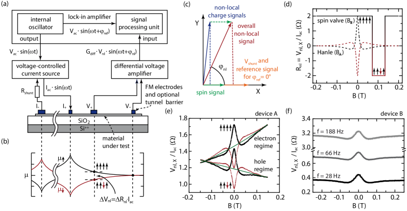
We discuss the mechanisms behind the occurrence of charge-induced, non-local voltages using the example of a lateral spin-valve device whose non-local signal is measured with a lock-in technique (Fig. 1a). But we note that many of the discussed charge-induced signals also occur in other measurement techniques (including DC measurements) and other device geometries (e.g. Hall bar structures for the non-local detection of the spin Hall effect). In our example the sinusoidal voltage signal from the internal oscillator of the lock-in amplifier is used as a reference signal for a voltage-to-current-converter. This converter is driving a current through the device under test (DUT) between the two ferromagnetic electrodes in the injection circuit denoted I+ and I-. It is assumed that the voltage-to-current-converter only creates a negligible phase shift between the reference voltage and the current through the device (probed e.g. by the voltage drop over a shunt resistor ).
The applied charge current gets spin-polarized by the ferromagnetic electrodes and therefore creates a spin accumulation in the material right below the electrodes [1, 2, 3]. This is depicted as a quasi-chemical potential for each spin orientation in Fig. 1b. Because of the gradient in the spin accumulation, spins also diffuse from the I+ electrode towards the non-local part of the device. The corresponding spin accumulation in this part decreases exponentially because of relaxation processes and can be probed between the spin-sensitive, ferromagnetic electrodes (V+ and V-) with a differential voltage amplifier [1, 2, 3].
If the DUT has a spin diffusion coefficient , the time that is needed for the spins to diffuse a distance into the non-local region is on the order of (e.g. for the majority of reported spin transport experiments in graphene this time is between 500 ps and 10 ns). In typical measurements this time is several orders of magnitude shorter than the period of the applied AC signal. Therefore, there cannot be any measurable phase that is caused by spin diffusion between the applied AC current, which creates the spin accumulation in the first place, and the measured non-local spin signal. Accordingly, any non-local signal that has a phase is either due to a measurement artifact or is linked to a physical phenomenon that is not connected to spins. In this respect a lock-in amplifier now becomes important, as it can decompose the overall non-local signal in contributions that are in-phase and out-of-phase to its internal oscillator (Fig. 1c). The X-channel (sometimes also called Re- or Real-channel) of the lock-in measures the amplitude of the non-local voltage that is in-phase to the internal oscillator, whereas the Y-channel (Im- or Imag-channel) measures the signal that is shifted by 90∘. According to the above explanation the spin signal should be entirely located within the X-channel of the lock-in (green arrow in Fig. 1c).
In Fig. 1d the theoretically expected curves for a spin valve and a Hanle spin precession measurement are depicted for the case that only the bare spin signal is present in a non-local measurement. For the spin valve measurement the magnetic field is applied in plane to the material and anti-parallel to the magnetization of the ferromagnetic electrodes. Different widths of the electrodes lead to different coercive fields because of shape anisotropy [41, 42]. In Figs. 1b and 1d it is assumed that electrode V+ switches first (the four arrows represent the magnetisation direction going from electrode I- to V-). Therefore, V+ will no longer probe the spin up but rather the spin down potential, which should only lead to a sign reversal of the measured voltage (see detailed explanation with theoretical derivation in Refs. [1, 2, 3]). If the non-local resistance is calculated by normalizing the non-local voltage by the applied current, the corresponding spin valve curve should be perfectly centered around (Fig. 1d). If the magnetic field is applied in the out-of-plane direction, Hanle spin precession curves can be measured both in case of a parallel orientation of the respective magnetization directions of the I+ and V+ electrodes (black dashed curve in Fig. 1d) and the respective anti-parallel orientation (red dashed curve). These curves are expected to be mirror images of each other and they should converge to zero at high magnetic fields because of a complete dephasing of the spins [1, 2, 3].
Instead, Fig. 1e depicts typical experimental Hanle curves with obvious charge-related background signals that are measured in both the hole and the electron regime of a graphene-based spin valve device (see discussion in section IV how the occurrence of these spurious signals may change for other materials and device structures, e.g. metallic spin valve devices). The background signal can be easily calculated by the arithmetic mean of the two curves for parallel and anti-parallel orientation (green curves in Fig. 1e) and can be fitted by a second order polynomial function. Subtracting this background from the measured data results in Hanle curves as depicted in Fig. 1d, i.e. curves that are perfectly centered around and can be well-fitted with models that only consider a spin signal [1, 2, 3]. It was shown that this kind of magnetic-field dependent background signal can be explained by a combination of a current-spreading effect and the Hall effect [43, 19], the latter causing the slope to change when tuning the device from the hole into the electron regime.
To highlight the previously described background signal whose amplitude increases towards higher frequencies, we use another graphene-based spin valve device for the sake of simplicity. For this device the current spreading effect was minimized by improving the device fabrication process (see explanation in section II.1). As a result the corresponding Hanle curves in Fig. 1f do not have a magnetic-field dependent background signal. Instead, it is seen how a constant offset voltage increases for increasing frequencies of the applied current. It should be noted that in Fig. 1f only the projection of the underlying charge-induced, non-local voltage in the X-channel is depicted (compare to blue arrow in Fig. 1c). As explained in the following sections, the underlying charge-induced signal exhibits a phase close to 90∘. Accordingly, the signal in the Y-channel increases significantly more, even pushing the channel into an overload condition for frequencies higher than 188 Hz in case of this device, which eventually leads to measurement artefacts of the spin signal in the X-channel.
There are a variety of reasons for trying to prevent such charge-induced signals from appearing in non-local measurements. The most obvious ones are that such signals can no longer be falsely attributed to spin-related effects and that the analysis of the spin data gets much simpler. Additionally, there is also the benefit to improve the signal-to-noise ratio of the spin measurement via three effects: First, the gain of the differential voltage amplifier and the sensitivity of the lock-in amplifier can be optimized for the amplitude of the spin signal. Second, preventing a flow of charges in the non-local detection circuit will also prevent that such currents can contribute noise to the measurement. Third, to be able to increase the measurement frequency opens the possibility to probe the spin signal in low-noise frequency bands far away from e.g. the 1/f-noise at low frequencies or typical interference frequencies of 50 Hz or 60 Hz.
II Overview of non-local charge signals
Besides the actual spin signal , there are at least seven other contributions to the overall non-local signal that will be discussed in detail in the following sections:
| (1) |
These contributions can be divided into two groups: The first group consists of signals that are inherent to the device structure and/or the measurement setup and are caused by current spreading (), thermo-electric voltages (), input bias currents (), or crosstalk and interference signals (). These four signals are normally quite insensitive to changes of the common-mode voltage in the transport channel, as explained in more detail in the Supporting Information [44]. Therefore, the current source that is presented in this study will only have minor influence on these signals. Instead, the second group consists of charge-induced signals that are caused by the common-mode voltage within the non-local detection circuit. Therefore, our current source can be used to minimize their impact on non-local spin transport measurements. This group includes signals that are caused by leakage currents (), a finite common-mode rejection ratio (), and the signal that scales with the measurement frequency and that can be explained by charging currents of capacitances in the detection circuit ().
We note that the respective contribution of each charge-related signal can vary quite significantly depending on details like device fabrication, properties of the investigated material, device geometry, measurement setup, and measurement technique. Usually, there are one or two dominating charge-related signals, whereas others might only get relevant for the most precise measurements, for which voltage signals slightly above the thermal noise floor are to be measured. In section II.10 we discuss how a magnetic field dependent measurement can be used to determine the charge-induced contribution to the total non-local signal and how this contribution can then be subtracted from the measurement to obtain the bare spin signal. Additionally, we explain possible pitfalls that may occur in such a procedure.
II.1 Current Spreading ()
One of the most documented charge signals unfortunately does not have a consistent name convention, but instead can be found by different names in literature, such as ”current spreading”, ”baseline resistance”, or simply ”ohmic contribution” [45, 43, 18, 19, 46, 47, 35]. Common to all publications about this charge signal is a spatially inhomogeneous, non-uniform injection of the charge current into the DUT, either via a side-arm of a Hall bar structure or a pinhole in the tunnel barrier of the injection electrode. This is illustrated in Fig. 2a in which I- drains the current and V- detects any voltage uniformly over the whole width of the DUT. Electrode I+ instead injects the current in a point-like manner, breaking the spatial symmetry. A small part of the sourced current will flow on a curved path from I+ into the non-local part of the device before it eventually flows into I-. This leads to a non-uniform potential landscape in the non-local part of the device (colored lines illustrate equipotential lines; actual simulations of this effect can be found in Refs. [43, 19, 35, 48]). This non-uniform potential landscape results in a potential difference between the two voltage probes V+ and V- (especially if V+ also probes in a point-like manner).
An out-of-plane magnetic field (as applied in a Hanle spin precession measurement) acts on the charge currents via a Lorentz force that modifies the potential landscape and therefore the measured non-local voltage (an illustration of the resulting change in the potential landscape is shown by dashed lines in Fig. 2a). Numerical simulations have shown that this Hall-like effect can explain the background signal in Fig. 1e that depends both on the magnetic field and the charge carrier density [43, 19]. In case of a Hall bar geometry, the magnitude of the non-local charge signal at can be estimated by the van der Pauw theorem to [18]:
| (2) |
with the applied current , the two-dimensional sheet resistance , the distance between the sidearm at which the current is injected and the sidearm at which the non-local voltage is probed, and the width of the transport channel.
We are not aware of a measurement technique that can minimize the contribution of to the overall non-local signal. Nevertheless, certain changes in the fabrication process can minimize this charge signal. Foremost, according to equation 2 an increase in the aspect ratio can significantly reduce the effect of current spreading both in case of Hall bar and spin valve geometries. As both the signal due to current spreading and the spin signal decay exponentially with the distance between the I+ and V+ electrodes [1, 2, 3], it is especially the width of the transport channel that should be minimized. Only applicable to the spin valve geometry is the improvement of the interface between the ferromagnetic electrode and the material under test (e.g. by minimizing pinholes in a tunnel barrier), to increase the uniformity of the charge carrier injection over the whole width of the transport channel.
II.2 Thermoelectric voltages ()
It is well-documented that thermo-electric and even magneto-thermo-electric effects can cause non-local charge signals via a combination of Joule heating, the Peltier effect, the Seebeck effect, the Ettingshausen effect, or the Nernst effect [49, 50, 51, 52, 53, 54, 46, 55]. The heat that is generated by the flow of charge carriers between the injection electrodes I+ and I- (Fig. 1a) creates a temperature gradient along the non-local part of the device, especially as electrodes V+ and V- can act as heat sinks. This temperature gradient then results in a differential voltage via e.g. the Seebeck or Nernst effect [49, 50, 51, 52, 53, 54, 55].
The heat that is created by the flow of charge carriers in the injection circuit can depend both linearly (e.g. in case of the Peltier effect) or quadratically (e.g. in case of Joule heating) on the applied current. Hence, in a lock-in measurement the resulting thermoelectric signal can appear both at the first and the second harmonic of the excitation frequency of the current [49, 50]. To our knowledge, no phase shift is observed between the applied current and the thermally induced voltage. This is consistent to the thermal diffusivity of typical materials that are used for spin transport devices [56, 57]. These thermal diffusivities yield heat transfer times over the whole device that are several orders of magnitude shorter than the period of typically applied AC signals (see similar discussion about the spin diffusion coefficient in section I).
Because of the inherent nature of thermoelectric voltages, we are not aware of measurement methods that can reduce their contribution after device fabrication. A suppression of these spurious signals can only occur by design choices during the fabrication process, like the design of electrodes that may function as heat sinks, the heat conductivity of the underlying substrate, or the design of the I+ and I- electrodes in such a way that their respective Peltier effects cancel each other to some extent [54, 46, 55].
Finally, it is important to note that thermoelectric signals not only depend on gate-induced changes in the transport properties of the DUT [58, 59], but that there are even magnetic field dependent analogs to the Peltier and Seebeck effects, whiche are the Ettingshausen and Nernst effects, respectively. These two effects can result in a -field dependence of the corresponding non-local, thermoelectric signal [49, 52, 51].
II.3 Input bias currents ()
We now assume that no current source is connected to the device and that the electrodes I+ and I- are shorted to GND. The only equipment that is connected to the DUT via electrodes V+ and V- is either a differential voltage amplifier or a lock-in amplifier. But even in this situation a small current will flow through the device. This is due to currents that are flowing either out of or into the inputs of a voltage or a lock-in amplifier. Especially in case of operational amplifiers or instrumentation amplifiers this current is called input bias current [60, 61, 62]. In a transport measurement these input bias currents result in non-local charge currents and, therefore, generate voltage drops within the device.
The input bias currents differ by several orders of magnitude between different measurement equipments. Because of high input bias currents up to the nA or even A range, standard amplifiers that use bipolar junction transistors (BJT) in their input stages are unsuitable for non-local spin measurements. However, precision amplifiers may include internal circuitry that diminishes the input bias currents of BJT inputs down to the higher pA range. Even lower input bias currents in the lower pA or even fA range [63] can be found in amplifiers that use field-effect transistors (FET). However, even this type of amplifier might cause problems, as a damage to the input stages may increase these currents significantly.
It is a-priori not clear if the charge signal that is caused by input bias currents is relevant in a non-local spin measurement. We recommend to measure both the input bias currents and the the common-mode rejection ratio (see section II.7) of the experimental setup to clarify this point. In the Supplemental Material [44] we give more information about such measurement procedures and discuss why input bias currents are normally only relevant for DC measurements.
II.4 Crosstalk and interference signals ()
There is always a certain coupling between different signal lines within a measurement setup. Especially cryogenic measurement systems, for which unshielded cables are often placed close together over longer distances [64], can exhibit non-negligible capacitive coupling between individual lines. An AC signal, like the bias voltage that drives the current through the injection circuit, can therefore couple into the wires that are connecting the V+ and V- electrodes to the measurement equipment outside the cryostat. Everything that will change the amplitude of the bias voltage, like a gate-induced change in the conductance of the DUT or a magnetoresistance effect, can change the amplitude of the signal that is coupled into the non-local detection circuit.
Wires can also be prone to damages to their insulation, which can yield reduced insulation resistances between different lines. Leakage currents directly between wires of the injection and detection circuit can therefore result in spurious signals in case of both AC and DC measurements. Fortunately, such setup-related signals can be easily identified by measuring the impedances between each line without any installed DUT.
Interference signals that couple from external sources into the measurement setup can also result in spurious, non-local signals. A common but erroneous assumption is that radio frequency (RF) signals do not impact DC or lock-in measurements, as in the first case the signal is averaged over time-scales several orders of magnitude longer than the period of the RF signal and in the second case the lock-in only measures a signal within a very narrow band around the excitation frequency. But as long as there are non-linear components within the measurement circuit, a down-mixing of the RF interference signal occurs. As a result, RF signals are known to e.g. create DC offset voltages in amplifier circuits [65, 66, 67].
II.5 Common-mode voltage and virtual ground
All of the non-local charge signals, which are discussed in the following sections, significantly depend on the so-called common-mode voltage in the non-local part of the device. This is the voltage that is common to both inputs (non-inverting (+) and inverting (-) input) of the differential amplifier that is connected to electrodes V+ and V-. If we denote these input voltages as , then the common-mode voltage is defined as:
| (3) |
To simplify the discussion on this matter, we make several assumptions that should apply well to a majority of devices. However, these assumptions should be carefully examined considering own device schemes and measurement techniques.
We assume that the frequency of the applied AC current is low enough that any inductance or capacitance of the DUT can be neglected, while the measurement setup can still exhibit inductances or capacitances. The analog assumption in case of a DC measurement is that the time step between two measurement points is much longer than the settling time that is caused by the inductance or capacitance of the DUT. Accordingly, we model the equivalent circuit of the device by a series of ohmic resistors (Fig. 2b) where the contact resistances exhibit ohmic characteristics. Finally, we assume that the measurement system exhibits a well-defined ground potential (GND), that every voltage is referenced to this GND and that the shielding of any coaxial cables are put to the same GND.
To drive a current through the injection circuit, a current source has to apply the voltage
| (4) |
between electrodes I+ and I-. The easiest way to accomplish this is to put one of the electrodes to GND and to apply the full bias voltage (referenced to GND) to the other electrode (red letters in Fig. 2b). Because of the voltage divider that is built from , and , the material under test right below the injection electrode I+ will be on a potential that is unequal to zero, i.e. unequal to GND. Every measurement parameter that has an effect on one of the resistances , and will thus have an impact on . E.g. changing the conductivity of the material by tuning the charge carrier density via a gate voltage will change . Therefore, all spurious non-local signals that are caused by will show a gate-dependent behaviour.
If we neglect any charge currents and their associated ohmic voltage drops in the non-local part of the device, the same voltage is applied to both inputs of the differential voltage amplifier that is connected to electrodes V+ and V-. Under this condition the common-mode voltage would be equal to .
As explained in the following sections, several non-local signals are caused by this common-mode voltage. Fortunately, there is a quick way to check if is playing a role in a measurement. For the wiring denoted with the red letters in Fig. 2b, the measurement only has to be repeated after putting a high-ohmic resistor between the I- electrode and GND. The current-induced voltage drop over this additional resistor will lift the potential (measured against GND) in the whole circuit, therefore increasing . There is only one pitfall to this method, which is a general problem for non-zero common-mode voltages in devices in which the charge carrier density is controlled via electrostatic gating: Gate voltages are normally referenced to GND, but the gate-electric field effect does not depend on the absolute value of the gate voltages but the potential differences between the gates and the DUT. Changing is therefore also changing the gate-induced charge carrier densities (see Supplemental Material [44] for more information). If the spin-signal depends on the charge carrier density, it might be difficult to tell if a change in the non-local signal by lifting the non-local part of the DUT to another potential is related to either a change in the charge-carrier dependent spin signal or a change in the common-mode dependent spurious signals.
The current source that is presented in this work can significantly reduce the common-mode voltage by freely distributing the potential difference that is necessary to drive the current to the two injection electrodes (green letters in Fig. 2b):
| (5) |
with adjustable between (see in-depth technical discussion of the current source in the Supplemental Material [44]). Depending on the values of the ohmic voltage divider consisting of , and , there will be a certain value of for which the common-mode voltage is zero (). Although the non-local part of the device is not connected to GND, it will nevertheless be on ground potential at all times. The right choice of will therefore create a so-called virtual ground in the non-local part of the device. This not only nullifies the non-local charge signals that are caused by , but also results in the fact that any applied gate voltage (referenced to GND) is equal to the potential difference between gate and the non-local part of the DUT (see Supplemental Material [44] on how the adjustment of therefore also impacts a local four-probe measurement of the gate-dependent resistivity of graphene).
II.6 Voltages caused by leakage currents ()
The most obvious non-local charge signal that is caused by a common-mode voltage is due to leakage currents to GND. Especially the finite input impedances of measuring equipment ( in Fig. 2b) play a crucial role, but also more unexpected current paths to GND like damaged insulations of cables or broken capacitors. These leakage currents (red, dashed lines in Fig. 2b) create ohmic voltage drops over the resistances , and , which result in a non-local voltage between V+ and V-.
Assuming purely ohmic impedances and a voltage divider model, the amplitude of this non-local voltage scales linearly with the common-mode voltage and significantly depends on the relative magnitude of the leakage resistance to ground with respect to the resistances , and . Therefore, it is not surprising that spurious voltage signals due to leakage currents are mainly reported in measurements of high-impedance states (see Ref. [68] and the supplementary information of Refs. [10, 11]). Hence, the spurious signal can e.g. be much more pronounced in graphene-based spin valves, in which high-resistive tunnel barriers have to be incorporated to overcome the conductivity mismatch problem [69, 70, 71] compared to metallic spin valves without tunnel barriers.
In our work on graphene-based spin valves, we use a lock-in amplifier that has an input impedance of only to GND (SR830 from Stanford Research Systems). To reduce the effect of leakage currents, we use an additional differential amplifier (SR560 from Stanford Research Systems) with a higher input impedance of to probe the differential voltage between electrodes V+ and V- before the non-local signal is sent to the input of the lock-in (Fig. 1a). Some laboratory-grade multimeters and voltmeters even offer the possibility to select the input impedance to be either or . Repeating a non-local measurement with different input impedances can easily answer the question if the measured non-local voltage is partially caused by leakage currents. But the best solution is to avoid leakage currents entirely by creating a virtual ground inside the non-local part of the device. Under such conditions, the absence of a potential difference between the non-local part of the device and GND completely prevents leakage current from flowing.
II.7 Common mode rejection ratio ()
The output voltage of an ideal differential voltage amplifier, which has a differential gain of and is connected to electrodes V+ and V- (Fig. 1a), is given by:
| (6) |
However, the output voltage of a real differential amplifier also contains a contribution that is proportional to the average voltage at electrodes V+ and V- and that scales with the common-mode gain [60, 61, 72, 73, 68, 63]:
| (7) |
Neglecting any current-driven voltage drops in the non-local part of the device, the average voltage of electrodes V+ and V- is exactly the voltage that is denoted as the common-mode voltage in section II.5. Therefore, will appear in the non-local measurement, although strongly attenuated by the common-mode gain . Data sheets of measurement equipment often state the ratio between the differential and the common-mode gain, the so-called common mode rejection ratio ():
| (8) |
In some data sheets the is only given for a specific differential gain and measurement frequency. As the can depend quite significantly on these two parameters, it is always a good practice to measure the of the own setup at gains and frequencies used for the experiments.
II.8 Capacitor charging ()
All previously discussed signals are in phase with the current that is flowing in the injection circuit and are thus in phase with the spin signal. In contrast, the charge signal that is discussed in this section is phase-shifted to values close but unequal to 90∘. If a sinusoidal current is driven through the injection circuit, also and, therefore, the whole potential of the non-local part of the device will change sinusoidally over time. This is a problem as there are capacitances to GND in the non-local detection circuit ( and in Fig. 2b). Some of these capacitances are intentional, like the capacitors of RC low-pass filters, others are either parasitic or unavoidable, like capacitances to GND of the wiring (around 100 pF/m in case of coaxial cables) or the input capacitance of measurement equipment. As a result, the time-varying common-mode voltage will drive charge and discharge currents over these capacitors (dashed red lines in Fig. 2b).
The resulting differential voltage between V+ and V- can be best understood, if the combinations of the device resistances ( and ) and the setup capacitances () are seen as RC low-pass filters for the voltage in Fig. 2b. The respective RC time constants of the low-pass filters of the voltage probes V+ and V- typically differ, i.e.:
| (9) |
As a result, both the amplitude and the phase of the transmitted voltage signal will differ between the two inputs of the differential voltage amplifier. This leads to a partial conversion of the common-mode voltage into a differential voltage, which is a well-known phenomenon in electronics. Such a conversion is discussed in many application notes of analog-to-digital converters, where a mismatch in the capacitors of a common-mode filter can convert common-mode noise into differential noise. Another example is the conversion between common- and differential-mode voltages caused by imbalances in filters against electromagnetic interference [74, 75].
Although the voltage is caused by the charging currents of the capacitors and , it is nevertheless not perfectly at a phase of 90∘ relative to due to the ohmic resistances , , and . Therefore, also provides a contribution to the X-channel signal of the lock-in amplifier, which will be discussed in section III and can also be seen in simulations conducted with LTspice (models used for the simulations are available in Ref. [76]).
The amplitude of scales linearly with the measurement frequency (see section III), because the current that is caused by a voltage over a capacitor is given as:
| (10) |
This capacitor charging current also flows through the non-local part of the device. In general, is highly dependent on every change in the device’s resistances and capacitances: A change in , , or will change the value of and, therefore, also the voltage that will be applied to the capacitors and . On the other hand, every change in , , , , , or will have an impact on the RC time constants.
To minimize , the capacitances and should be minimized as much as possible, e.g. by reducing the length of the wiring from the V+ and V- electrodes or by avoiding any RC low-pass filters in the measurement setup. Furthermore, additional ohmic resistors might be put into series to the electrodes V+ and V- to roughly match the RC time constants by compensating varying contact resistances. But the best way to suppress is to set the whole non-local part of the device to a virtual ground. In such a case, there is no potential difference across the capacitors and and, therefore, no capacitor charging current.
II.10 Magnetic field dependent measurements
Magnetic field dependent transport measurements are usually performed to distinguish an actual spin signal from spurious charge signals. The success of such an approach significantly depends on two conditions:
-
1.
Does the spin signal exhibit a magnetic field dependence that significantly differs from the magnetic response of the charge-induced signals? The best case scenario here is the existence of a clear spin precession signal.
-
2.
Does the experiment allow to switch the orientation of the injected spins, e.g. by switching the magnetization of the ferromagnetic electrodes?
If both conditions are met, the most reliable way to mathematically remove any charge-induced contribution from the measured data is to record the Hanle spin precession curves for both parallel () and anti-parallel () orientations of the respective magnetization of the injection and detection electrodes. In the ideal case only the bare spin signal will change its sign when reversing the relative magnetization directions [1, 2]. Instead all other spin-independent, charge-induced signals in equation 1 should not change with the magnetization of the electrodes (exceptions are discussed further below). Therefore, the arithmetic mean of both measurements should yield the charge-induced background signal:
| (11) |
This is shown as the green line in Fig. 1e. Subtracting both measurements from each other should yield the pure spin signal:
| (12) |
Under such conditions the charge-induced signals should not pose any risk of a misinterpretation of the spin-dependent data. Nevertheless, the noise that is associated with the charge-induced signals cannot be removed by this subtraction method and, therefore, will deteriorate the signal-to-noise ratio of the spin signal.
It is important to note that equations 11 and 12 are no longer valid if the ferromagnetic electrodes exhibit fringe or stray fields that can act on the DUT. Such fields are well known to complicate the analysis of spin measurements [23, 77, 78, 79, 80, 81, 48] and can appear in quite different forms: 1.) As long as the width of the electrode is small enough that a single-domain magnetization prevails [42], fringe fields with relevant strengths should only be located at the electrode’s two faces that are normal to the electrode’s easy-axis [42, 82]. Stray fields can impact the measurement if these two faces are placed too close to or even on top of the transport channel [23, 77, 78]. 2.) If the width of the electrode is too wide, the magnetization can fall into a multi-domain structure that exhibits stray fields all along its different faces [42]. 3.) A magnetic field applied non-colinear to the electrode can rotate the magnetization from the electrode’s easy axis [41], possibly pushing fringe fields towards the transport channel. This can lead to a situation where fringe fields increasingly affect the DUT with increasing external magnetic field strength (see main text and supplementary information of Refs. [28, 83, 48]). 4.) Stray fields can also occur if the surface of the ferromagnet exhibits a great roughness, which e.g. can be caused by pinholes in a tunnel barrier that is separating the ferromagnet from the DUT [79, 80, 81]. 5.) Stray fields can also be created by domain walls that are pinned at steps in the ferromagnetic electrode. Even the small height difference between a substrate and the top of a single layer graphene spin valve was found to be large enough to be able to pin a domain wall [82].
Fringe or stray fields can become a real issue if there is no unmistakable signature of spin precession in a magnetic field dependent measurement. For example, in 3D topological insulators (TIs) spin precession in a non-local spin transport measurement is not expected because of the spin-momentum-locking [84]. This is the reason why only spin valve measurements are shown in a large number of publication about spin transport experiments in TIs [85, 86, 87, 88, 89, 90, 91]. In this context, it was indeed demonstrated that fringe-field-induced Hall voltages can create artefacts that resemble the switching signals that are expected from a current-induced spin polarization in TI-based spin valves [23, 77, 81].
If neither of the two above conditions is fulfilled, it is even more important to carefully analyze the non-local spin measurements to avoid a misinterpretation of the results. This is especially the case for non-local spin Hall experiments, where quite controversial results were published over the years [4]. In particular, reports about unexpectedly large spin Hall effects [92, 93, 94] often could not be reproduced in later studies that instead identified the role of charge-induced signals in the non-local measurement [18, 19, 20, 21, 22].
Unfortunately, many studies only consider the one charge-induced signal that contributes the most to the overall non-local signal. After subtracting this spurious signal from the measured data, it is then argued that the remaining signal has to be due to spins, especially when the signal shows a magnetic field dependence. However, quite a few charge-induced signals can also exhibit a magnetic field dependence: All charge currents that are flowing in the non-local part of the device, either caused by current spreading or leakage currents, experience the Hall effect. Furthermore, thermal voltages due to the Ettingshausen and Nerst effects show a magnetic field dependence. And finally, any magnetoresistive effect that changes the resistance of the DUT in the injection circuit ( in Fig. 2b) will have an impact on the common-mode voltage and, therefore, will change all charge-induced signals that depend on , i.e. (section II.6), (section II.7), (section II.3), and (section II.8). The magnetic-field-induced changes might be small, but so are the majority of measured non-local spin signals.
III Phase-shifted charge signal in lock-in measurements
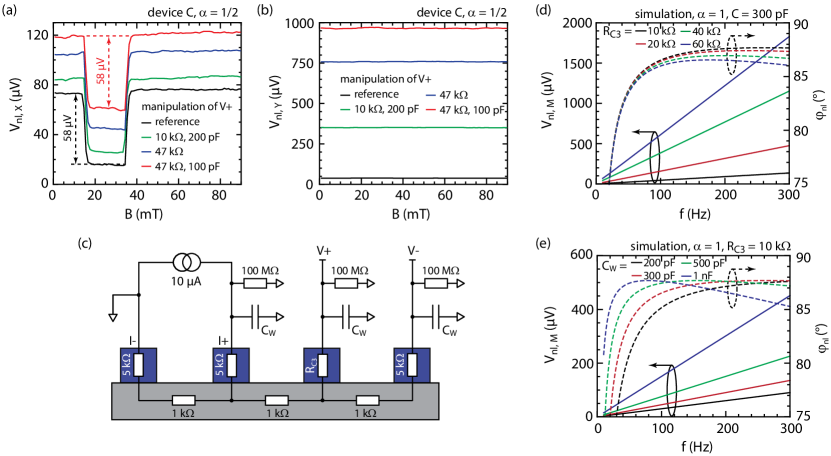
In this section, we discuss in detail the charge-induced non-local voltage signal that is caused by the charging and discharging currents of the capacitances in the non-local part of the setup (see section II.8). For this purpose, we measure graphene spin-valve devices with cobalt electrodes and either MgO or Al2O3 tunnel barriers (details on the exact device geometry and the fabrication process including flake transfer techniques, etching recipes in case of structured CVD-graphene devices, and metalization schemes can be found in Refs. [95, 36, 96, 37, 97, 98, 99]). Figs. 3a and 3b demonstrate how a change in the RC time constant of the V+ electrode has a direct impact on the spin-valve signal in both the X- and Y-channel. For this experiment was not adjusted to create a virtual ground in the non-local part of the device (see explanation in section II.5). Instead, was arbitrarily set to 1/2 which resulted in a non-vanishing common-mode voltage in this device (Fig. 2b).
The manipulation of the RC time constant was accomplished both by connecting ohmic resistors in series to the contact resistance of the V+ electrode (resistance values in Figs. 3a and 3b) and by increasing the length of the coaxial cable that is connecting the electrode to the differential voltage amplifier (100 pF per meter). These manipulations do not have any impact on the amplitude of the spin signal (switching in Fig. 3a indicated by the dashed arrows), but create an ever increasing offset in the signal of the X-channel. As the charge signal is shifted in phase by almost 90∘, the increase in the Y-channel signal (Fig. 3b) is significantly more pronounced. In fact, after applying a differential gain of by the voltage amplifier (see Fig. 1a), the voltage measured by the Y-channel of the lock-in eventually reaches 1 V, which is the maximum voltage before the input of the used lock-in goes into an overload condition.
Simulations conducted with LTspice [76] confirm the dependence of the non-local charge signal on variations in the resistances of the contacts and the capacitances of the wiring. The equivalent circuit for this simulation is shown in Fig. 3c, where either the contact resistance or the capacitance of the wiring is varied, whereas all other values are set to parameters typical for a graphene-based spin-valve device (LTspice files can be found in Ref. [76]). From the simulations the amplitude and the phase (see definitions in Fig. 1c) of the differential, non-local voltage is extracted as a function of the driving frequency of the current in the injection circuit. Fig. 3d shows the results for different values of and a fixed capacitance of , while Fig. 3e depicts the case with a fixed contact resistance but varying capacitances . Both cases demonstrate the linear increase in the amplitude of the non-local charge signal with the measurement frequency (see explanation in section II.8). Furthermore, the simulations demonstrate that the resulting non-local charge signal has a phase close to but not exactly at 90∘ due to the ohmic contributions. The strongly decreasing phase towards lower frequencies is caused by the frequency-independent leakage currents that are flowing over the finite input impedances which are modelled by the resistors (see section II.6). As soon as the signal that is caused by the capacitor charging becomes negligible towards , the leakage currents, which are in phase with the current in the injection circuit, eventually are dominating and are pushing the phase to zero.
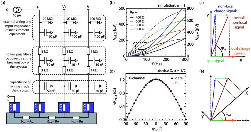
The experimental results and simulations shown in Fig. 3 demonstrate how much the measurement signal can depend on the wiring of the measurement setup. In particular, RC low pass filters can be extremely disadvantageous to non-local, lock-in-based measurements, as they significantly increase the total capacitance of the V+ and V- lines to GND. This in turn increases the spurious signals that are caused by the charging currents of the corresponding capacitors. We use the equivalent circuit that is shown in Fig. 4a to simulate how a mere change of the DUT’s resistances (, for ) impacts the non-local signal. In this equivalent circuit the charge signal was intentionally diminished by assuming identical values for contact resistances, capacitances of the wiring, and RC filter characteristics for all relevant contacts. Therefore, the only difference in the overall RC-time-constants of contacts V+ and V- is given by the value of . Of course, the resistance in the injection circuit also influences the common-mode voltage which is driving the non-local currents in the first place. In Fig. 4b the resulting non-local charge signals for both the X-channel (solid lines) and Y-channel (dashed lines) are plotted as a function of the measurement frequency for different values of . The results strikingly demonstrate how significantly the spurious non-local charge signal depends in this case even on gate-induced changes in the DUT’s resistivity. The simulations were conducted with an applied current of , therefore the left y-axis in Fig. 4b corresponds to a non-local resistance between 0 and .
The example of the RC filters illustrates how drastically specific details of the setup can influence such measurements. We therefore strongly advice to verify the basic assumptions that are often made for individual setups. One important assumption is that the spin signal is fully located within the X-channel of the lock-in. As discussed in section I, the spin signal should be in phase with the current in the injection circuit, which in turn should be in phase with the output signal from the lock-in’s internal oscillator (green and orange vectors in Fig. 4c). Instead the vector addition of all non-local charge signals results in a signal with a phase somewhere between 0∘ and 90∘ (blue vector in Fig. 4c).
Most lock-in amplifiers offer the possibility to rotate the X-Y-coordinate system by a reference phase relative to the internal oscillator, which is illustrated in Fig. 4e. The measured signals are then the projections of both the spin and charge signals onto the respective axis. The amplitude of the actual spin signal in the X-channel as a function of can be determined by the amplitude of the switching in a spin-valve measurement that is repeated for different [43]. In case of our setup and the newly designed current source, the result of such an experiment is shown in Fig. 4d. The actual data points (black squares) can be perfectly fitted (red line) with an equation that describes the projection of the spin signal onto the rotating X-axis:
| (13) |
with a maximum spin signal and an offset phase between the spin signal and the internal oscillator signal. The fit yields a value of , which demonstrates that our current source creates a current signal and, therefore, a spin signal that is almost perfectly in phase with the output of the lock-in.
Finally, we demonstrate the actual strength of such a current source: The distribution of the bias voltage between contacts I+ and I- can be controlled in a way, that the non-local part of the device is set to a virtual ground (see theoretical explanation in section II.5 and discussion about the technical operation of the current source in the Supplemental Material [44]). Under this condition the common-mode voltage in the non-local part is zero at all times (), i.e. no charge current can flow over any resistance or capacitance to GND. Furthermore, spurious signals due to a finite common-mode rejection ratio of the measurement setup are also minimized.
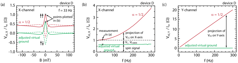
The impact of such an adjustment procedure on a Hanle measurement is shown in Fig. 5a. The particular device for this demonstration was chosen because it only exhibits a constant background signal, which is typical for the capacitor charging effect. The absence of a magnetic field dependent background indicates that the current spreading effect is largely diminished. The red lines depict Hanle curves in both parallel (solid lines) and anti-parallel (dashed lines) magnetization configurations of the I+ and V+ electrodes if a symmetric bias is applied to electrodes I+ and I- (, i.e. to I+ and to I-, compare to Fig. 2b). As the growth of uniform and reproducible tunnel barriers on the inert graphene is quite challenging [100, 101, 27, 102, 103], the difference in the respective contact resistances of I+ and I- is usually quite large. Therefore, the virtual ground point in case of a symmetric bias voltage normally does not lie within the transport channel of the DUT. Accordingly, there is a finite common-mode voltage driving the spurious non-local signals, which is seen as a background signal. Instead, the green curves in Fig. 5a depict the same Hanle measurement (recorded in the X-channel) after was adjusted in such a way that the signal in the Y-channel of the lock-in was minimized. With this adjustment also the background signal in the Hanle measurement has almost completely vanished (in the Supplemental Material [44] we demonstrate that adjusting until the signal in the Y-channel is minimized also avoids common-mode related artifacts in local measurements).
The dependence of the non-local signal on the frequency is depicted in Figs. 5b and 5c for the X-channel and Y-channel, respectively. For these graphs the values in the parallel configuration of the Hanle curves at were measured for both the symmetric (red) and the adjusted bias condition (green). In the Y-channel (Fig. 5c) the aforementioned linear increase of the charge-induced, non-local signal with increasing frequency can be observed in case of the symmetric bias condition. At a frequency of the charge-induced signal is already over 30x larger than the actual spin signal in the X-channel. For more unfavourable values of or in devices that have even more strongly varying contact resistances, the charge-induced signal can even be much larger. This and the fact that spin signals can be much smaller than the one presented in Fig. 5 can yield huge differences between the amplitudes of the spin and charge-induced signals of up to several orders of magnitude.
It is important to note that the charge-induced signal in Fig. 5c goes to zero for even in case of . This implies that the complete signal in the Y-channel is caused by the capacitor charging effect, as its amplitude scales linearly with the applied frequency (see explanation in section II.8). On the other hand, in Fig. 5b there is still an offset between the two curves for and the adjusted ground condition for (indicated by the dashed line). That means that there are additional charge-induced signals present in the X-channel, apart from the projection of onto the X-channel that is responsible for the increasing background signal towards higher frequencies. This increase is not linear as the one seen in Fig. 5c, because the overall phase of varies slightly with the applied frequency (see frequency-dependent phases in Figs. 3d and 3e, and the non-linear increase of the signal in the X-channel in Fig. 4b). Importantly, adjusting the virtual ground in such a way that the spurious signal in the Y-channel vanishes, also completely removes these additional signals within the X-channel, i.e. the green curve in Fig. 5b only consists of the actual spin signal. Therefore, the offset in case of for must be caused by the other charge-induced artifacts that depend on the common-mode voltage, namely and (see sections II.6 and II.7). These two signals can appear not only in AC but also DC () measurements (see Supplemental Material [44] for a more detailed discussion). The possibility to remove these spurious signals therefore demonstrates that the presented current source is also highly beneficial for DC measurements.
IV Conclusion
We have discussed seven different charge-induced, non-local voltage signals that can appear in a spin measurement, despite the fact that this measurement scheme is repeatedly claimed to be free of such spurious signals. However, it is important to emphasize that the relevance of each individual charge-induced signal can vary significantly depending on details in device fabrication, properties of the investigated material, device geometry, measurement setup, and measurement technique. In our study, we focused on experimental data that was measured with a lock-in based technique on graphene spin-valve devices. In such devices we observe that two charge-induced signals normally prevail: the signal that is caused by current-spreading (section II.1) and the signal that is caused by the capacitor charging currents (section II.8). These two signals dominate because tunnel barriers must be used in these devices to overcome the conductivity mismatch problem for an efficient spin injection [69, 70, 71]. But it is known that growing homogeneous, pinhole-free tunnel barriers on top of the inert graphene surface is quite challenging without damaging or modifying the underlying graphene [100, 101, 27, 102, 103]. Pinholes in the tunnel barrier promote the effect of current spreading, whereas strongly varying contact resistances lead to different RC time constants and, therefore, the signal that is caused by the capacitor charging currents. Furthermore, when tunnel barriers are present, a larger bias voltage must be applied to drive the same current as without barriers. Without the possibility to adjust the virtual ground, this unavoidably also increases the common-mode voltage (Fig. 2b) and, therefore, all non-local charge signals that are driven by . In devices without tunnel barriers the relative contribution of each individual charge-induced signal may be completely different.
Nevertheless, the occurrence of all these different charge-induced signals is a general problem, as in the past these artifacts may have been falsely attributed to a variety of spin- or valley-related transport phenomena. For example, it has already been reported that measurement artifacts have most likely led to erroneous and misleading claims regarding the value of the spin Hall angle in certain materials or the spin transport properties of topological insulators. Therefore, understanding both the origins of these signals and the specific conditions under which they can appear is crucial for the correct analysis of non-local transport experiments, not only in the field of spintronics but also other newly emerging fields as valleytronics. If available, we have discussed ways how these spurious signals can be minimized. In particular, we demonstrated that our current source, that is able to create a virtual ground in the non-local part of the device, can remove any charge-induced signals that are caused by a common-mode voltage.
Acknowledgements.
This project has received funding from the European Union’s Horizon 2020 research and innovation programme under grant agreement No. 881603 (Graphene Flagship) and the Deutsche Forschungsgemeinschaft (DFG, German Research Foundation) under Germany’s Excellence Strategy - Cluster of Excellence Matter and Light for Quantum Computing (ML4Q) EXC 2004/1 - 390534769, through DFG (BE 2441/9-1 and STA 1146/11-1), and by the Helmholtz Nano Facility (HNF) [104] at the Forschungszentrum Jülich.References
- Žutić et al. [2004] I. Žutić, J. Fabian, and S. Das Sarma, Spintronics: Fundamentals and applications, Reviews of Modern Physics 76, 323 (2004).
- Fabian et al. [2007] J. Fabian, A. Matos-Abiague, C. Ertler, P. Stano, and I. Žutić, Semiconductor spintronics, Acta Physica Slovaca 57, 565 (2007).
- Johnson and Silsbee [1988] M. Johnson and R. H. Silsbee, Coupling of electronic charge and spin at a ferromagnetic-paramagnetic metal interface, Physical Review B 37, 5312 (1988).
- Sinova et al. [2015] J. Sinova, S. O. Valenzuela, J. Wunderlich, C. H. Back, and T. Jungwirth, Spin Hall effects, Reviews of Modern Physics 87, 1213 (2015).
- Hirohata et al. [2020] A. Hirohata, K. Yamada, Y. Nakatani, I.-L. Prejbeanu, B. Diény, P. Pirro, and B. Hillebrands, Review on spintronics: Principles and device applications, Journal of Magnetism and Magnetic Materials 509, 166711 (2020).
- Roche et al. [2015] S. Roche, J. Åkerman, B. Beschoten, J.-C. Charlier, M. Chshiev, S. P. Dash, B. Dlubak, J. Fabian, A. Fert, M. Guimarães, F. Guinea, I. Grigorieva, C. Schönenberger, P. Seneor, C. Stampfer, S. O. Valenzuela, X. Waintal, and B. van Wees, Graphene spintronics: the European Flagship perspective, 2D Materials 2, 030202 (2015).
- Avsar et al. [2020] A. Avsar, H. Ochoa, F. Guinea, B. Özyilmaz, B. J. van Wees, and I. J. Vera-Marun, Colloquium: Spintronics in graphene and other two-dimensional materials, Reviews of Modern Physics 92, 021003 (2020).
- Sierra et al. [2021] J. F. Sierra, J. Fabian, R. K. Kawakami, S. Roche, and S. O. Valenzuela, Van der Waals heterostructures for spintronics and opto-spintronics, Nature Nanotechnology 16, 856 (2021).
- Gorbachev R. et al. [2014] V. Gorbachev R., W. Song J. C., L. Yu G., V. Kretinin A., F. Withers, Y. Cao, A. Mishchenko, V. Grigorieva I., S. Novoselov K., S. Levitov L., and K. Geim A., Detecting topological currents in graphene superlattices, Science 346, 448 (2014).
- Sui et al. [2015] M. Sui, G. Chen, L. Ma, W.-Y. Shan, D. Tian, K. Watanabe, T. Taniguchi, X. Jin, W. Yao, D. Xiao, and Y. Zhang, Gate-tunable topological valley transport in bilayer graphene, Nature Physics 11, 1027 (2015).
- Shimazaki et al. [2015] Y. Shimazaki, M. Yamamoto, I. V. Borzenets, K. Watanabe, T. Taniguchi, and S. Tarucha, Generation and detection of pure valley current by electrically induced Berry curvature in bilayer graphene, Nature Physics 11, 1032 (2015).
- Endo et al. [2019] K. Endo, K. Komatsu, T. Iwasaki, E. Watanabe, D. Tsuya, K. Watanabe, T. Taniguchi, Y. Noguchi, Y. Wakayama, Y. Morita, and S. Moriyama, Topological valley currents in bilayer graphene/hexagonal boron nitride superlattices, Applied Physics Letters 114, 243105 (2019).
- Ribeiro et al. [2017] M. Ribeiro, S. R. Power, S. Roche, L. E. Hueso, and F. Casanova, Scale-invariant large nonlocality in polycrystalline graphene, Nature Communications 8, 2198 (2017).
- Marmolejo-Tejada et al. [2018] J. M. Marmolejo-Tejada, J. H. García, M. D. Petrović, P.-H. Chang, X.-L. Sheng, A. Cresti, P. Plecháč, S. Roche, and B. K. Nikolić, Deciphering the origin of nonlocal resistance in multiterminal graphene on hexagonal-boron-nitride with ab initio quantum transport: Fermi surface edge currents rather than Fermi sea topological valley currents, Journal of Physics: Materials 1, 015006 (2018).
- Aharon-Steinberg et al. [2021] A. Aharon-Steinberg, A. Marguerite, D. J. Perello, K. Bagani, T. Holder, Y. Myasoedov, L. S. Levitov, A. K. Geim, and E. Zeldov, Long-range nontopological edge currents in charge-neutral graphene, Nature 593, 528 (2021).
- Foa-Torres and Valenzuela [2021] L. Foa-Torres and S. Valenzuela, A valley of opportunities, Physics World November, 43 (2021).
- Roche et al. [2022] S. Roche, S. R. Power, B. K. Nikolić, J. H. García, and A.-P. Jauho, Have mysterious topological valley currents been observed in graphene superlattices?, Journal of Physics: Materials 5, 021001 (2022).
- Mihajlović et al. [2009] G. Mihajlović, J. E. Pearson, M. A. Garcia, S. D. Bader, and A. Hoffmann, Negative Nonlocal Resistance in Mesoscopic Gold Hall Bars: Absence of the Giant Spin Hall Effect, Physical Review Letters 103, 166601 (2009).
- Völkl et al. [2019] T. Völkl, D. Kochan, T. Ebnet, S. Ringer, D. Schiermeier, P. Nagler, T. Korn, C. Schüller, J. Fabian, D. Weiss, and J. Eroms, Absence of a giant spin Hall effect in plasma-hydrogenated graphene, Physical Review B 99, 085401 (2019).
- Kaverzin and van Wees [2015] A. A. Kaverzin and B. J. van Wees, Electron transport nonlocality in monolayer graphene modified with hydrogen silsesquioxane polymerization, Physical Review B 91, 165412 (2015).
- Van Tuan et al. [2016] D. Van Tuan, J. M. Marmolejo-Tejada, X. Waintal, B. K. Nikolić, S. O. Valenzuela, and S. Roche, Spin Hall Effect and Origins of Nonlocal Resistance in Adatom-Decorated Graphene, Physical Review Letters 117, 176602 (2016).
- Wang et al. [2015] Y. Wang, X. Cai, J. Reutt-Robey, and M. S. Fuhrer, Neutral-current Hall effects in disordered graphene, Physical Review B 92, 161411 (2015).
- de Vries et al. [2015] E. K. de Vries, A. M. Kamerbeek, N. Koirala, M. Brahlek, M. Salehi, S. Oh, B. J. van Wees, and T. Banerjee, Towards the understanding of the origin of charge-current-induced spin voltage signals in the topological insulator , Physical Review B 92, 201102 (2015).
- Kamalakar et al. [2015] M. V. Kamalakar, C. Groenveld, A. Dankert, and S. P. Dash, Long distance spin communication in chemical vapour deposited graphene, Nature Communications 6, 6766 (2015).
- Yan et al. [2016] W. Yan, O. Txoperena, R. Llopis, H. Dery, L. E. Hueso, and F. Casanova, A two-dimensional spin field-effect switch, Nature Communications 7, 13372 (2016).
- Xu et al. [2018] J. Xu, T. Zhu, Y. K. Luo, Y.-M. Lu, and R. K. Kawakami, Strong and Tunable Spin-Lifetime Anisotropy in Dual-Gated Bilayer Graphene, Physical Review Letters 121, 127703 (2018).
- Cubukcu et al. [2015] M. Cubukcu, M.-B. Martin, P. Laczkowski, C. Vergnaud, A. Marty, J.-P. Attané, P. Seneor, A. Anane, C. Deranlot, A. Fert, S. Auffret, C. Ducruet, L. Notin, L. Vila, and M. Jamet, Ferromagnetic tunnel contacts to graphene: Contact resistance and spin signal, Journal of Applied Physics 117, 083909 (2015).
- Ghiasi et al. [2019] T. S. Ghiasi, A. A. Kaverzin, P. J. Blah, and B. J. van Wees, Charge-to-Spin Conversion by the Rashba-Edelstein Effect in Two-Dimensional van der Waals Heterostructures up to Room Temperature, Nano Letters 19, 5959 (2019).
- Amamou et al. [2018] W. Amamou, G. Stecklein, S. J. Koester, P. A. Crowell, and R. K. Kawakami, Spin Absorption by In Situ Deposited Nanoscale Magnets on Graphene Spin Valves, Physical Review Applied 10, 044050 (2018).
- Ringer et al. [2018a] S. Ringer, M. Rosenauer, T. Völkl, M. Kadur, F. Hopperdietzel, D. Weiss, and J. Eroms, Spin field-effect transistor action via tunable polarization of the spin injection in a Co/MgO/graphene contact, Applied Physics Letters 113, 132403 (2018a).
- Zhu et al. [2018] T. Zhu, S. Singh, J. Katoch, H. Wen, K. Belashchenko, I. Žutić, and R. K. Kawakami, Probing tunneling spin injection into graphene via bias dependence, Physical Review B 98, 054412 (2018).
- Gebeyehu et al. [2019] Z. M. Gebeyehu, S. Parui, J. F. Sierra, M. Timmermans, M. J. Esplandiu, S. Brems, C. Huyghebaert, K. Garello, M. V. Costache, and S. O. Valenzuela, Spin communication over 30 m long channels of chemical vapor deposited graphene on SiO2, 2D Materials 6, 034003 (2019).
- Safeer et al. [2019] C. K. Safeer, J. Ingla-Aynés, F. Herling, J. H. Garcia, M. Vila, N. Ontoso, M. R. Calvo, S. Roche, L. E. Hueso, and F. Casanova, Room-Temperature Spin Hall Effect in Graphene/MoS2 van der Waals Heterostructures, Nano Letters 19, 1074 (2019).
- Zhao et al. [2019] B. Zhao, D. Khokhriakov, B. Karpiak, A. M. Hoque, L. Xu, L. Shen, Y. P. Feng, X. Xu, Y. Jiang, and S. P. Dash, Electrically controlled spin-switch and evolution of Hanle spin precession in graphene, 2D Materials 6, 035042 (2019).
- Liu et al. [2019] Y. Liu, C. Zeng, J. Ding, J. Zhong, Y. Gao, X. Kuang, J. Yu, L. Cao, J. He, and Z. Liu, Effect of the low-resistance tunnel barriers induced inhomogeneous spin current distribution in graphene crossed configuration lateral spin valve, AIP Advances 9, 115005 (2019).
- Drögeler et al. [2016] M. Drögeler, C. Franzen, F. Volmer, T. Pohlmann, L. Banszerus, M. Wolter, K. Watanabe, T. Taniguchi, C. Stampfer, and B. Beschoten, Spin Lifetimes Exceeding 12 ns in Graphene Nonlocal Spin Valve Devices, Nano Letters 16, 3533 (2016).
- Volmer et al. [2014] F. Volmer, M. Drögeler, E. Maynicke, N. von den Driesch, M. L. Boschen, G. Güntherodt, C. Stampfer, and B. Beschoten, Suppression of contact-induced spin dephasing in graphene/MgO/Co spin-valve devices by successive oxygen treatments, Physical Review B 90, 165403 (2014).
- Benítez et al. [2020] L. A. Benítez, W. Savero Torres, J. F. Sierra, M. Timmermans, J. H. Garcia, S. Roche, M. V. Costache, and S. O. Valenzuela, Tunable room-temperature spin galvanic and spin Hall effects in van der Waals heterostructures, Nature Materials 19, 170 (2020).
- Panda et al. [2020] J. Panda, M. Ramu, O. Karis, T. Sarkar, and M. V. Kamalakar, Ultimate Spin Currents in Commercial Chemical Vapor Deposited Graphene, ACS Nano 14, 12771 (2020).
- Ringer et al. [2018b] S. Ringer, S. Hartl, M. Rosenauer, T. Völkl, M. Kadur, F. Hopperdietzel, D. Weiss, and J. Eroms, Measuring anisotropic spin relaxation in graphene, Physical Review B 97, 205439 (2018b).
- Brands and Dumpich [2005] M. Brands and G. Dumpich, Experimental determination of anisotropy and demagnetizing factors of single Co nanowires by magnetoresistance measurements, Journal of Applied Physics 98, 014309 (2005).
- Leven and Dumpich [2005] B. Leven and G. Dumpich, Resistance behavior and magnetization reversal analysis of individual Co nanowires, Physical Review B 71, 064411 (2005).
- Volmer et al. [2015] F. Volmer, M. Drögeler, T. Pohlmann, G. Güntherodt, C. Stampfer, and B. Beschoten, Contact-induced charge contributions to non-local spin transport measurements in Co/MgO/graphene devices, 2D Materials 2, 024001 (2015).
- [44] The Supplemental Material includes 1.) a discussion of all technical aspects of the voltage-controlled current source with all information necessary to rebuild the electronic, 2.) measurements about its accuracy, bandwidth, and stability during fast transients, 3.) a discussion and measurements of how a common mode voltage can impact even local measurements, 4.) practical hints on how to adjust the virtual ground, 5.) a discussion about applications and limitations of the current source, and 6.) some practical advices both on the use of the current source and on the investigation of the charge-induced signals in non-local measurements.
- Johnson and Silsbee [2007] M. Johnson and R. H. Silsbee, Calculation of nonlocal baseline resistance in a quasi-one-dimensional wire, Physical Review B 76, 153107 (2007).
- Hu et al. [2019] J. Hu, G. Stecklein, D. A. Deen, Q. Su, P. A. Crowell, and S. J. Koester, Scaling of the Nonlocal Spin and Baseline Resistances in Graphene Lateral Spin Valves, IEEE Transactions on Electron Devices 66, 5003 (2019).
- Rüffer et al. [2011] D. Rüffer, F. D. Czeschka, R. Gross, and S. T. B. Goennenwein, Experimental observation of an enhanced anisotropic magnetoresistance in non-local configuration, Applied Physics Letters 99, 142112 (2011).
- Safeer et al. [2021] C. K. Safeer, F. Herling, W. Y. Choi, N. Ontoso, J. Ingla-Aynés, L. E. Hueso, and F. Casanova, Reliability of spin-to-charge conversion measurements in graphene-based lateral spin valves, 2D Materials 9, 015024 (2021).
- Renard et al. [2014] J. Renard, M. Studer, and J. A. Folk, Origins of Nonlocality Near the Neutrality Point in Graphene, Physical Review Letters 112, 116601 (2014).
- Bakker et al. [2010] F. L. Bakker, A. Slachter, J.-P. Adam, and B. J. van Wees, Interplay of Peltier and Seebeck Effects in Nanoscale Nonlocal Spin Valves, Physical Review Letters 105, 136601 (2010).
- Das et al. [2016] K. S. Das, F. K. Dejene, B. J. van Wees, and I. J. Vera-Marun, Anisotropic Hanle line shape via magnetothermoelectric phenomena, Physical Review B 94, 180403 (2016).
- Gopinadhan et al. [2015] K. Gopinadhan, Y. J. Shin, R. Jalil, T. Venkatesan, A. K. Geim, A. H. C. Neto, and H. Yang, Extremely large magnetoresistance in few-layer graphene/boron-nitride heterostructures, Nature Communications 6, 8337 (2015).
- Hu and Kimura [2013] S. Hu and T. Kimura, Anomalous Nernst-Ettingshausen effect in nonlocal spin valve measurement under high-bias current injection, Physical Review B 87, 014424 (2013).
- Bennet et al. [2019] R. K. Bennet, A. Hojem, and B. L. Zink, Thermal gradients and anomalous Nernst effects in membrane-supported nonlocal spin valves, Physical Review B 100, 104404 (2019).
- Ariki et al. [2017] T. Ariki, T. Nomura, K. Ohnishi, and T. Kimura, Effective suppression of thermoelectric voltage in nonlocal spin-valve measurement, Applied Physics Express 10, 063004 (2017).
- Yang et al. [2012] N. Yang, X. Xu, G. Zhang, and B. Li, Thermal transport in nanostructures, AIP Advances 2, 041410 (2012).
- Balandin [2011] A. A. Balandin, Thermal properties of graphene and nanostructured carbon materials, Nature Materials 10, 569 (2011).
- Zuev et al. [2009] Y. M. Zuev, W. Chang, and P. Kim, Thermoelectric and Magnetothermoelectric Transport Measurements of Graphene, Physical Review Letters 102, 096807 (2009).
- Harzheim et al. [2020] A. Harzheim, C. Evangeli, O. V. Kolosov, and P. Gehring, Direct mapping of local Seebeck coefficient in 2D material nanostructures via scanning thermal gate microscopy, 2D Materials 7, 041004 (2020).
- Gray et al. [2009] P. R. Gray, P. J. Hurst, S. H. Lewis, and R. G. Meyer, Analysis and Design of Analog Integrated Circuits (John Wiley & Sons, Inc., Hoboken, NJ, USA, 2009).
- Gray and Meyer [1982] P. R. Gray and R. G. Meyer, MOS operational amplifier design - a tutorial overview, IEEE Journal of Solid-State Circuits 17, 969 (1982).
- Kinget [2005] P. R. Kinget, Device mismatch and tradeoffs in the design of analog circuits, IEEE Journal of Solid-State Circuits 40, 1212 (2005).
- Märki et al. [2017] P. Märki, B. A. Braem, and T. Ihn, Temperature-stabilized differential amplifier for low-noise DC measurements, Review of Scientific Instruments 88, 085106 (2017).
- Ekin [2010] J. Ekin, Experimental Techniques for Low-Temperature Measurements: Cryostat Design, Material Properties and Superconductor Critical-Current Testing (Oxford Scholarship Online, 2010).
- Fiori and Crovetti [2002] F. Fiori and P. S. Crovetti, Nonlinear effects of radio-frequency interference in operational amplifiers, IEEE Transactions on Circuits and Systems I: Fundamental Theory and Applications 49, 367 (2002).
- Poulton [1994] A. Poulton, Effect of conducted EMI on the DC performance of operational amplifiers, Electronics Letters 30, 282 (1994).
- Redouté and Steyaert [2007] J.-M. Redouté and M. Steyaert, Measurement of EMI induced input offset voltage of an operational amplifier, Electronics Letters 43, 1088 (2007).
- De Sanctis et al. [2018] A. De Sanctis, J. D. Mehew, S. Alkhalifa, C. P. Tate, A. White, A. R. Woodgate, M. F. Craciun, and S. Russo, Novel circuit design for high-impedance and non-local electrical measurements of two-dimensional materials, Review of Scientific Instruments 89, 024705 (2018).
- Rashba [2000] E. I. Rashba, Theory of electrical spin injection: Tunnel contacts as a solution of the conductivity mismatch problem, Physical Review B 62, R16267 (2000).
- Schmidt et al. [2000] G. Schmidt, D. Ferrand, L. W. Molenkamp, A. T. Filip, and B. J. van Wees, Fundamental obstacle for electrical spin injection from a ferromagnetic metal into a diffusive semiconductor, Physical Review B 62, R4790 (2000).
- Fert and Jaffrès [2001] A. Fert and H. Jaffrès, Conditions for efficient spin injection from a ferromagnetic metal into a semiconductor, Physical Review B 64, 184420 (2001).
- Szynowski [1983] J. Szynowski, CMRR analysis of instrumentation amplifiers, Electronics Letters 19, 547 (1983).
- Pallas-Areny and Webster [1991] R. Pallas-Areny and J. G. Webster, Common mode rejection ratio in differential amplifiers, IEEE Transactions on Instrumentation and Measurement 40, 669 (1991).
- Wang and Lee [2010] S. Wang and F. C. Lee, Investigation of the Transformation Between Differential-Mode and Common-Mode Noises in an EMI Filter Due to Unbalance, IEEE Transactions on Electromagnetic Compatibility 52, 578 (2010).
- Ott [2009] H. W. Ott, Electromagnetic Compatibility Engineering (John Wiley & Sons, Inc., Hoboken, NJ, USA, 2009).
- [76] The data supporting the findings of this study are available in a Zenodo repository under https://doi.org/10.5281/zenodo.6525020. There we provide 1.) all data presented in each figure, 2.) the LTspice models for each simulation, 3.) Gerber files of the PCB used for our current source, 4.) the corresponding Altium Designer files, and 5.) a bill of materials.
- Karpiak et al. [2017] B. Karpiak, A. Dankert, A. W. Cummings, S. R. Power, S. Roche, and S. P. Dash, 1D ferromagnetic edge contacts to 2D graphene/h-BN heterostructures, 2D Materials 5, 014001 (2017).
- Groen et al. [2021] I. Groen, V. T. Pham, N. Leo, A. Marty, L. E. Hueso, and F. Casanova, Disentangling Spin, Anomalous, and Planar Hall Effects in Ferromagnet-Heavy-Metal Nanostructures, Physical Review Applied 15, 044010 (2021).
- Txoperena and Casanova [2016] O. Txoperena and F. Casanova, Spin injection and local magnetoresistance effects in three-terminal devices, Journal of Physics D: Applied Physics 49, 133001 (2016).
- Dash et al. [2011] S. P. Dash, S. Sharma, J. C. Le Breton, J. Peiro, H. Jaffrès, J.-M. George, A. Lemaître, and R. Jansen, Spin precession and inverted Hanle effect in a semiconductor near a finite-roughness ferromagnetic interface, Physical Review B 84, 054410 (2011).
- Muduli et al. [2012] P. K. Muduli, J. Barzola-Quiquia, S. Dusari, A. Ballestar, F. Bern, W. Böhlmann, and P. Esquinazi, Large local Hall effect in pin-hole dominated multigraphene spin-valves, Nanotechnology 24, 015703 (2012).
- Berger et al. [2015] A. J. Berger, M. R. Page, H. Wen, K. M. McCreary, V. P. Bhallamudi, R. K. Kawakami, and P. Chris Hammel, Correlating spin transport and electrode magnetization in a graphene spin valve: Simultaneous magnetic microscopy and non-local measurements, Applied Physics Letters 107, 142406 (2015).
- Li et al. [2020] L. Li, J. Zhang, G. Myeong, W. Shin, H. Lim, B. Kim, S. Kim, T. Jin, S. Cavill, B. S. Kim, C. Kim, J. Lischner, A. Ferreira, and S. Cho, Gate-Tunable Reversible Rashba-Edelstein Effect in a Few-Layer Graphene/2H-TaS2 Heterostructure at Room Temperature, ACS Nano 14, 5251 (2020).
- Hasan and Kane [2010] M. Z. Hasan and C. L. Kane, Colloquium: Topological insulators, Reviews of Modern Physics 82, 3045 (2010).
- Li et al. [2014] C. H. Li, O. M. J. van ‘t Erve, J. T. Robinson, Y. Liu, L. Li, and B. T. Jonker, Electrical detection of charge-current-induced spin polarization due to spin-momentum locking in Bi2Se3, Nature Nanotechnology 9, 218 (2014).
- Tang et al. [2014] J. Tang, L.-T. Chang, X. Kou, K. Murata, E. S. Choi, M. Lang, Y. Fan, Y. Jiang, M. Montazeri, W. Jiang, Y. Wang, L. He, and K. L. Wang, Electrical Detection of Spin-Polarized Surface States Conduction in (Bi0.53Sb0.47)2Te3 Topological Insulator, Nano Letters 14, 5423 (2014).
- Ando et al. [2014] Y. Ando, T. Hamasaki, T. Kurokawa, K. Ichiba, F. Yang, M. Novak, S. Sasaki, K. Segawa, Y. Ando, and M. Shiraishi, Electrical Detection of the Spin Polarization Due to Charge Flow in the Surface State of the Topological Insulator Bi1.5Sb0.5Te1.7Se1.3, Nano Letters 14, 6226 (2014).
- Dankert et al. [2015] A. Dankert, J. Geurs, M. V. Kamalakar, S. Charpentier, and S. P. Dash, Room Temperature Electrical Detection of Spin Polarized Currents in Topological Insulators, Nano Letters 15, 7976 (2015).
- Tian et al. [2015] J. Tian, I. Miotkowski, S. Hong, and Y. P. Chen, Electrical injection and detection of spin-polarized currents in topological insulator Bi2Te2Se, Scientific Reports 5, 14293 (2015).
- Lee et al. [2015] J. S. Lee, A. Richardella, D. R. Hickey, K. A. Mkhoyan, and N. Samarth, Mapping the chemical potential dependence of current-induced spin polarization in a topological insulator, Physical Review B 92, 155312 (2015).
- Yang et al. [2016] F. Yang, S. Ghatak, A. A. Taskin, K. Segawa, Y. Ando, M. Shiraishi, Y. Kanai, K. Matsumoto, A. Rosch, and Y. Ando, Switching of charge-current-induced spin polarization in the topological insulator , Physical Review B 94, 075304 (2016).
- Seki et al. [2008] T. Seki, Y. Hasegawa, S. Mitani, S. Takahashi, H. Imamura, S. Maekawa, J. Nitta, and K. Takanashi, Giant spin Hall effect in perpendicularly spin-polarized FePt/Au devices, Nature Materials 7, 125 (2008).
- Balakrishnan et al. [2013] J. Balakrishnan, G. Kok Wai Koon, M. Jaiswal, A. H. Castro Neto, and B. Özyilmaz, Colossal enhancement of spin-orbit coupling in weakly hydrogenated graphene, Nature Physics 9, 284 (2013).
- Balakrishnan et al. [2014] J. Balakrishnan, G. K. W. Koon, A. Avsar, Y. Ho, J. H. Lee, M. Jaiswal, S.-J. Baeck, J.-H. Ahn, A. Ferreira, M. A. Cazalilla, A. H. C. Neto, and B. Özyilmaz, Giant spin Hall effect in graphene grown by chemical vapour deposition, Nature Communications 5, 4748 (2014).
- Drögeler et al. [2014] M. Drögeler, F. Volmer, M. Wolter, B. Terrés, K. Watanabe, T. Taniguchi, G. Güntherodt, C. Stampfer, and B. Beschoten, Nanosecond Spin Lifetimes in Single- and Few-Layer Graphene-hBN Heterostructures at Room Temperature, Nano Letters 14, 6050 (2014).
- Volmer et al. [2021] F. Volmer, I. Seidler, T. Bisswanger, J.-S. Tu, L. R. Schreiber, C. Stampfer, and B. Beschoten, How to solve problems in micro- and nanofabrication caused by the emission of electrons and charged metal atoms during e-beam evaporation, Journal of Physics D: Applied Physics 54, 225304 (2021).
- Drögeler et al. [2017] M. Drögeler, L. Banszerus, F. Volmer, T. Taniguchi, K. Watanabe, B. Beschoten, and C. Stampfer, Dry-transferred CVD graphene for inverted spin valve devices, Applied Physics Letters 111, 152402 (2017).
- Drögeler et al. [2015] M. Drögeler, F. Volmer, M. Wolter, K. Watanabe, T. Taniguchi, D. Neumaier, C. Stampfer, and B. Beschoten, Nanosecond spin lifetimes in bottom-up fabricated bilayer graphene spin-valves with atomic layer deposited AlO spin injection and detection barriers, physica status solidi (b) 252, 2395 (2015).
- Bisswanger et al. [2021] T. Bisswanger, Z. Winter, A. Schmidt, F. Volmer, K. Watanabe, T. Taniguchi, C. Stampfer, and B. Beschoten, CVD bilayer graphene spin valves with 26 m spin diffusion length at room temperature, arXiv (2021), arXiv:2105.06277 .
- Canto et al. [2015] B. Canto, C. P. Gouvea, B. S. Archanjo, J. E. Schmidt, and D. L. Baptista, On the Structural and Chemical Characteristics of Co/Al2O3/graphene Interfaces for Graphene Spintronic Devices, Scientific Reports 5, 14332 (2015).
- Vervuurt et al. [2017] R. H. J. Vervuurt, W. M. M. E. Kessels, and A. A. Bol, Atomic Layer Deposition for Graphene Device Integration, Advanced Materials Interfaces 4, 1700232 (2017).
- Hsu et al. [2014] A. L. Hsu, R. J. Koch, M. T. Ong, W. Fang, M. Hofmann, K. K. Kim, T. Seyller, M. S. Dresselhaus, E. J. Reed, J. Kong, and T. Palacios, Surface-Induced Hybridization between Graphene and Titanium, ACS Nano 8, 7704 (2014).
- Ahlberg et al. [2016] P. Ahlberg, F. O. L. Johansson, Z.-B. Zhang, U. Jansson, S.-L. Zhang, A. Lindblad, and T. Nyberg, Defect formation in graphene during low-energy ion bombardment, APL Materials 4, 046104 (2016).
- HNF [2017] Research Center Jülich GmbH, HNF - Helmholtz Nano Facility, J. Large Scale Res. Facil. (JLSRF) 3, A112 (2017).