Ultrafast tunable lasers using lithium niobate integrated photonics
Recent advances in the processing of thin-film lithium niobate (LiNbO3) on insulator (LNOI) have enabled low-loss photonic integrated circuits [1, 2], modulators with improved half-wave voltage [3, 4], electro-optic frequency combs [5] and novel on-chip electro-optic devices, with applications ranging from 5G telecommunication [6] and microwave photonics [7] to microwave-to-optical quantum interfaces [8, 9]. Lithium niobate integrated photonic circuits could equally be the basis of integrated frequency-agile lasers with narrow linewidth. Pioneering work on polished lithium niobate crystal resonators [10, 11, 12] has led to the development of electrically tunable narrow-linewidth lasers [13]. Here we report low-noise frequency-agile lasers based on lithium niobate integrated photonics and demonstrate their use for coherent laser ranging. This is achieved through heterogeneous integration of ultra-low-loss silicon nitride (Si3N4) photonic circuits [14] with thin-film lithium niobate via direct wafer bonding. The hybrid platform features low propagation loss of 8.5 dB/m enabling narrow-linewidth lasing (intrinsic linewidth of 3 kHz) by self-injection locking to a III–V semiconductor laser diode. The hybrid mode of the resonator allows electro-optical laser frequency tuning at a speed of 12 petahertz/s ( Hz/s) with high linearity, low hysteresis and while retaining narrow linewidth. Using this hybrid integrated laser, we perform a proof-of-concept frequency-modulated continuous-wave (FMCW) LiDAR ranging experiment, with a resolution of 15 cm. By fully leveraging the high electro-optic coefficient of lithium niobate, with further improvements in photonic integrated circuits design, these devices can operate with CMOS-compatible voltages, or achieve millimetre-scale distance resolution. Endowing low loss silicon nitride integrated photonics with lithium niobate, gives a platform with wide transparency window, that can be used to realize ultrafast tunable lasers from the visible to the mid-infrared, with applications ranging from optical coherence tomography (OCT) and LiDAR to environmental sensing.
Lithium niobate is an attractive material for electro-optic devices, and has been widely used for many decades. It exhibits a transparency window from ultraviolet to mid-infrared wavelengths and has a large Pockels coefficient [15, 16], which is key for efficient, low-voltage, and high-speed modulation. Integrated photonics based on materials exhibiting the Pockels effect — such as AlN [17] and GaP [18] — have been demonstrated before, but only recently for lithium niobate [19, 20]. Following the commercial availability of lithium niobate on insulator via wafer bonding and smart-cut, there has also been substantial progress in the etching of low-loss lithium niobate waveguides, culminating in linear optical loss of 2.7 dB/m and ring resonators with intrinsic Q-factor of [1]. The majority of works have utilized argon ion beam etching to manufacture ridge waveguide structures, which enabled modulators operating at CMOS voltages [3], high-efficiency QPSK modulators [21], as well as electro-optic frequency combs [5]. In addition, the platform has provided a route to creating interfaces using cavity electro-optics that efficiently couple microwave to optical fields [9, 8]. Further potential applications include the creation of synthetic dimensions for topological photonics [22]. In addition to direct etching, recently also heterogeneous integration [23, 24] of lithium niobate chiplets onto silicon nitride [25] or silicon (Si) [26] integrated photonic circuits has been demonstrated.
Beyond application for electro-optical modulators, an integrated photonics platform with a large Pockels coefficient and low propagation loss fulfils all the requirements for realizing integrated frequency-agile laser sources, which feature fast, linear and mode-hop-free tuning. Specifically, such frequency-agile electro-optical lasers can be realized by self-injection locking of a III–V diode laser to an high-Q optical cavity [27]. This technique, in conjunction with low-loss integrated photonic resonators, has already enabled compact chip-scale lasers with Lorentzian linewidth on the order of one hertz using silicon nitride [28]. Yet to date, no integrated hybrid lasers based on materials displaying Pockels effect have been demonstrated. In contrast to thermal or piezoelectrical [29, 30] tuning of optical microresonators, electro-optical materials can enable ultra-fast optical tuning with theoretically tens of GHz intracavity modulation bandwidth. Integrated electro-optical materials can therefore be used to realize a host of laser structures, such as widely tunable Vernier lasers [31] or fast, mode-hop-free and continuously tunable lasers for a multitude of applications that include coherent LiDAR [32, 33, 34], trace-gas spectroscopy [35, 36], and optical coherence tomography (OCT) [37].
Here, we demonstrate for the first time a self-injection-locked narrow-linewidth frequency-agile laser based on a lithium niobate integrated photonic circuit. This is achieved on a heterogeneous integrated lithium niobate platform combining low-loss silicon nitride photonic waveguides with lithium niobate by wafer-scale bonding [38]. Damascene silicon nitride waveguides feature tight confinement, ultra-low propagation loss (1 dB/m), and high-power handling [14]. They can be manufactured with high yield on a wafer scale and are already available from a commercial foundry. Additional advantages of the silicon nitride waveguide platform include low gain of Raman and Brillouin nonlinearities [39, 40] and radiation hardness [41]. Our heterogeneous integrated lithium niobate on Damascene silicon nitride (LNOD) platform enables high-Q resonances (loaded linewidth 100 MHz), provides a high yield of bonded devices, and exhibits low (compared to ridge LNOI) insertion loss (3.9 dB per facet [38]). Combining the unique properties of both platforms enables self-injection locking with laser frequency noise reduction of 20 dB, a fundamental linewidth of 3 kHz, and frequency-agility with a flat actuation bandwidth up to 100 MHz. Using this hybrid integrated laser source, we perform FMCW LiDAR experiments in lab environment with resolution of 15 cm.
RESULTS
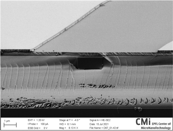
Heterogeneous integration of lithium niobate on silicon nitride. Our fabrication method combines the processes of photonic Damascene waveguide fabrication with wafer-scale bonding [42, 43] to enable electro-optic modulation on passive, ultralow-loss silicon nitride PICs, as schematically depicted in Fig. 1(a). Our process starts with the fabrication of a patterned and planarized silicon nitride substrate using the photonic Damascene process [44, 14]. Deep-ultraviolet (DUV) stepper lithography is used to pattern waveguides and microresonators on a silicon substrate with 4 m thick thermal wet silicon dioxide (SiO2). The pattern is then dry-etched into the silicon dioxide layer to form the waveguide preform, followed by a high-temperature reflow of the waveguide preform [45] to reduce surface roughness. Stoichiometric silicon nitride is deposited by low-pressure chemical vapour deposition (LPCVD) on the patterned substrate, filling the preform and forming the waveguide cores. Chemical mechanical polishing (CMP) is used to remove excess silicon nitride and to planarize the wafer top surface. Subsequently the entire substrate is thermally annealed at 1,200∘C to drive out the residual hydrogen contained in the silicon nitride. A silicon dioxide interlayer is deposited on the substrate, followed by densification. The interlayer is then polished to reduce the remaining topography and set the desired thickness. A root-mean-square roughness of less than 0.4 nm over an area of a few square micrometres and of only a few nanometres over an area of several hundred micrometres are necessary for bonding. Next, a few-nanometre-thick alumina layer is deposited by atomic layer deposition (ALD) on both the donor (LNOI) and the acceptor (Damascene) wafers before contact bonding and donor-wafer removal. Tungsten (W) electrodes are then manufactured by sputtering and reactive ion etching. At this point, the areas of the coupling facets and the tapered sections of the silicon nitride waveguides are cleared from lithium niobate by physical etching with argon ions, so that light can first couple into the tapered waveguides with minimal coupling losses, before transitioning to the area with lithium niobate bonded on top. Finally, chip release is performed by chip-facet definition by deep silicon dioxide and silicon etching, followed by chip separation through backside silicon lapping. Fig. 1(b) depicts a scanning electron microscope (SEM) cross section of the heterogeneous LNOD waveguide.
Laser self-injection locking. Laser self-injection locking is initiated by butt-coupling of an InP distributed-feedback (DFB) diode laser to the LNOD chip (Fig. 1 (c,d)) and tuning the laser current to match the output frequency to the resonance frequency of the LNOD resonator. The optical backreflection on surface or volumetric inhomogeneities inside the microresonator provides spectrally narrowband feedback to the laser diode by coupling clock- and counterclockwise propagating modes. Light in the counterclockwise mode radiates back to the laser bearing the power fraction given by the reflection coefficient , which depends on the interaction strength of the modes and the resonator coupling efficiency [46].
The laser diode is forced to oscillate at the frequency of the cavity resonance in the self-injection-locked regime. Assuming that the frequency noise of the laser is white, the frequency noise suppression ratio is [27]:
| (1) |
where is the linewidth of the free-running DFB laser; is the linewidth of self-injection-locked DFB laser; and are the quality factors of the laser diode cavity and of the microresonator mode, respectively (with , where and are the intrinsic cavity decay rate and bus–waveguide coupling rate); and is the phase-amplitude coupling factor [47]. Self-injection locking occurs within a finite frequency interval around the cavity resonance. The locking bandwidth is given, assuming large intermodal interaction strength and high coupling efficiency, by:
| (2) |
In order to strongly reduce the laser linewidth and increase the frequency locking range, a high-Q resonance and strong reflection are desirable.
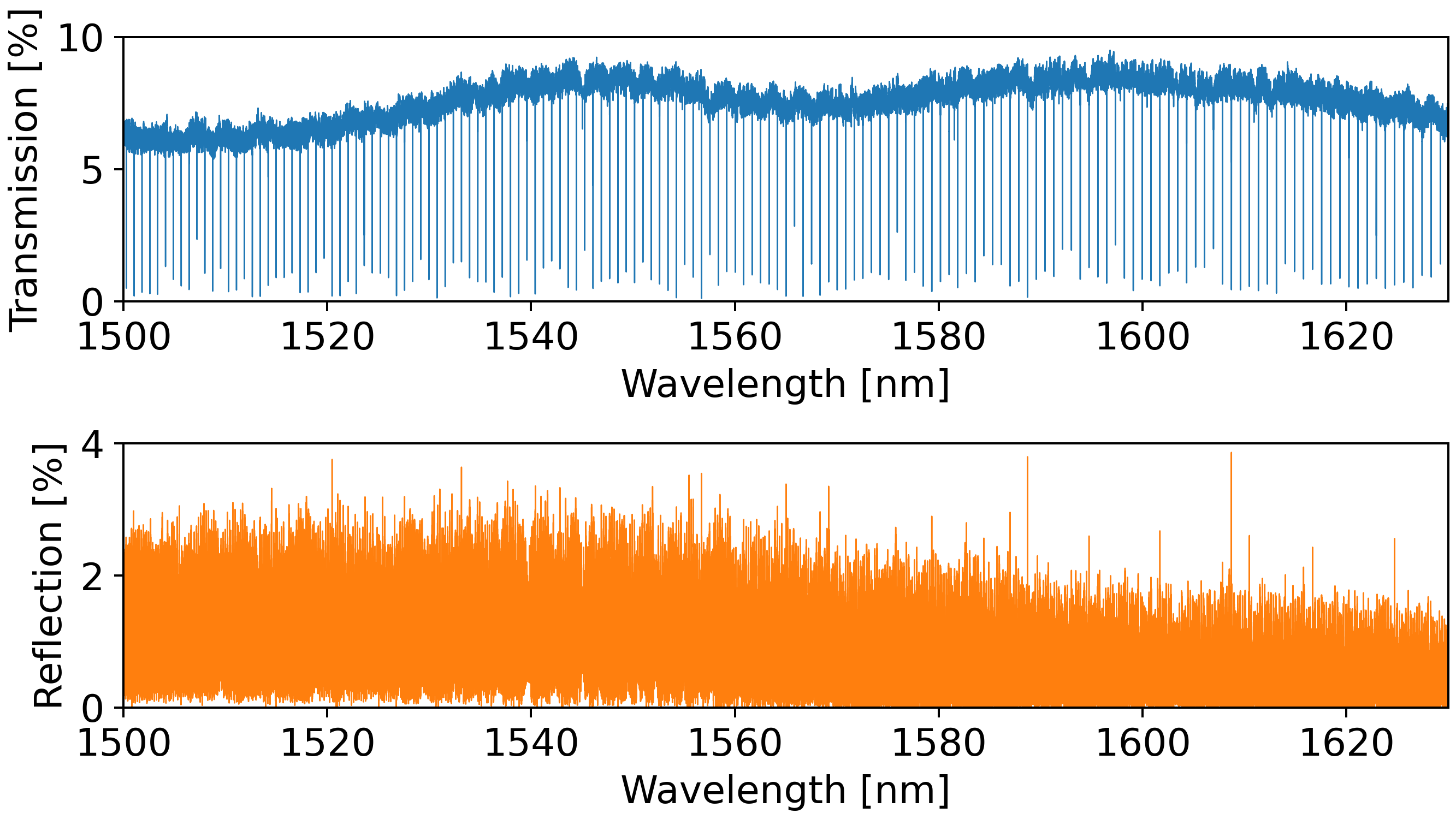
The device used in our experiments features a 102-GHz free spectral range (FSR) and a resonance linewidth of 100 MHz (see Fig. 2(a,b)) operated close to critical coupling.
The intrinsic loss of the microresonator indicates a linear propagation loss of our LNOD waveguide platform of 8.5 dB/m.
The power reflection of the device reaches 3% (see Fig. 2(a) and Supplementary Figure 2 for full spectrum) and features both the narrowband reflection of the microresonator and wideband sinusoidal modulation by spurious reflections from the chip facet, as well as and the transitions between the inverse tapers the LNOD waveguide.
Despite the weak back-reflection contrast, injection locking is observed due to the narrow linewidth of the optical resonance.
The self-injection-locked DFB emission spectrum (Fig. 2(c)) indicates a lasing wavelength of 1555.4 nm with a side-mode-suppression ratio of 50 dB.
To characterize self-injection locking, a heterodyne beat note of the unlocked and locked DFB laser with a reference laser (Toptica CTL) is generated on a fast photodiode and processed using an electrical spectrum analyzer (Fig. 2(d)).
We observe the narrowing of the beat note upon locking of the DFB laser (see Fig. 2(e)).
When sweeping the DFB current, we found the regions where there is almost no change of the laser frequency, because of the self-injection locking (see Fig. 2(f)).
To reveal the locking bandwidth, we set the DFB current inside the locked state, and scanned the cavity resonance by applying a triangular voltage chirp to the electrodes (Fig. 2(g)).
The self-injection locking is achieved within a frequency span of around 1 GHz; however, linear tuning is observed only within a 600-MHz band, due to the low back-reflection of the LNOD microresonator.
Next, we measured the frequency noise single-sideband spectral density of the DFB diode laser in the free-running and self-injection-locked regimes (see Methods for details and Figure 2(h) for results).
The laser self-injection locking suppresses the frequency noise by at least 20 dB across all frequency offsets.
We find the intersection point of the frequency noise curve and the beta-line [48] at 30 kHz (Fig. 2(h) orange and dashed red).
The full width at half maximum linewidth, which is calculated by integration of the frequency noise from the beta-line to the inverse integration time, is 56 kHz at 0.1 ms integration time, 262 kHz at 1 ms, and 1.1 MHz at 100 ms.
The laser frequency noise reaches a horizontal plateau (white noise floor) of 103 Hz2/Hz at 3 MHz offset, which corresponds to an intrinsic laser linewidth of 3.14 kHz.
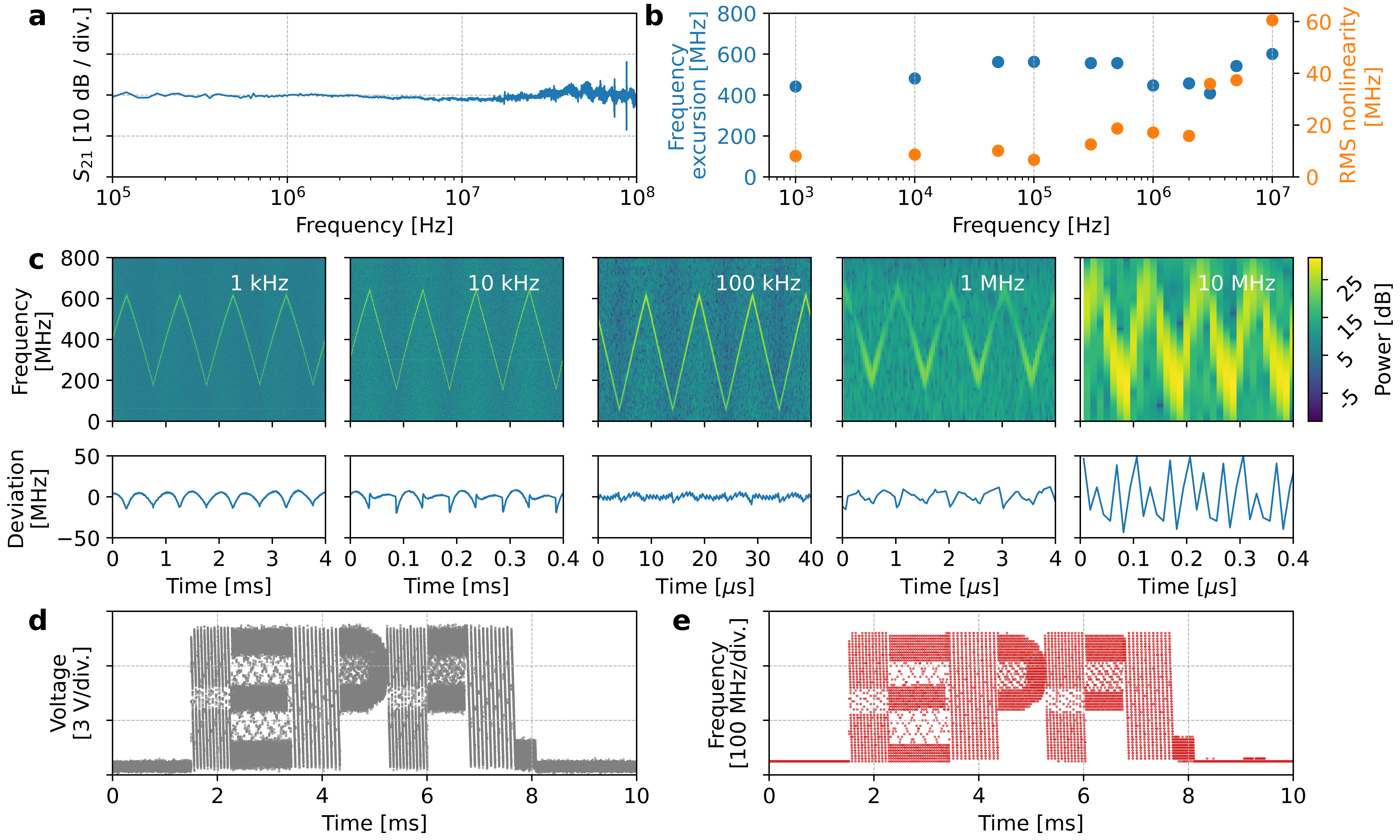
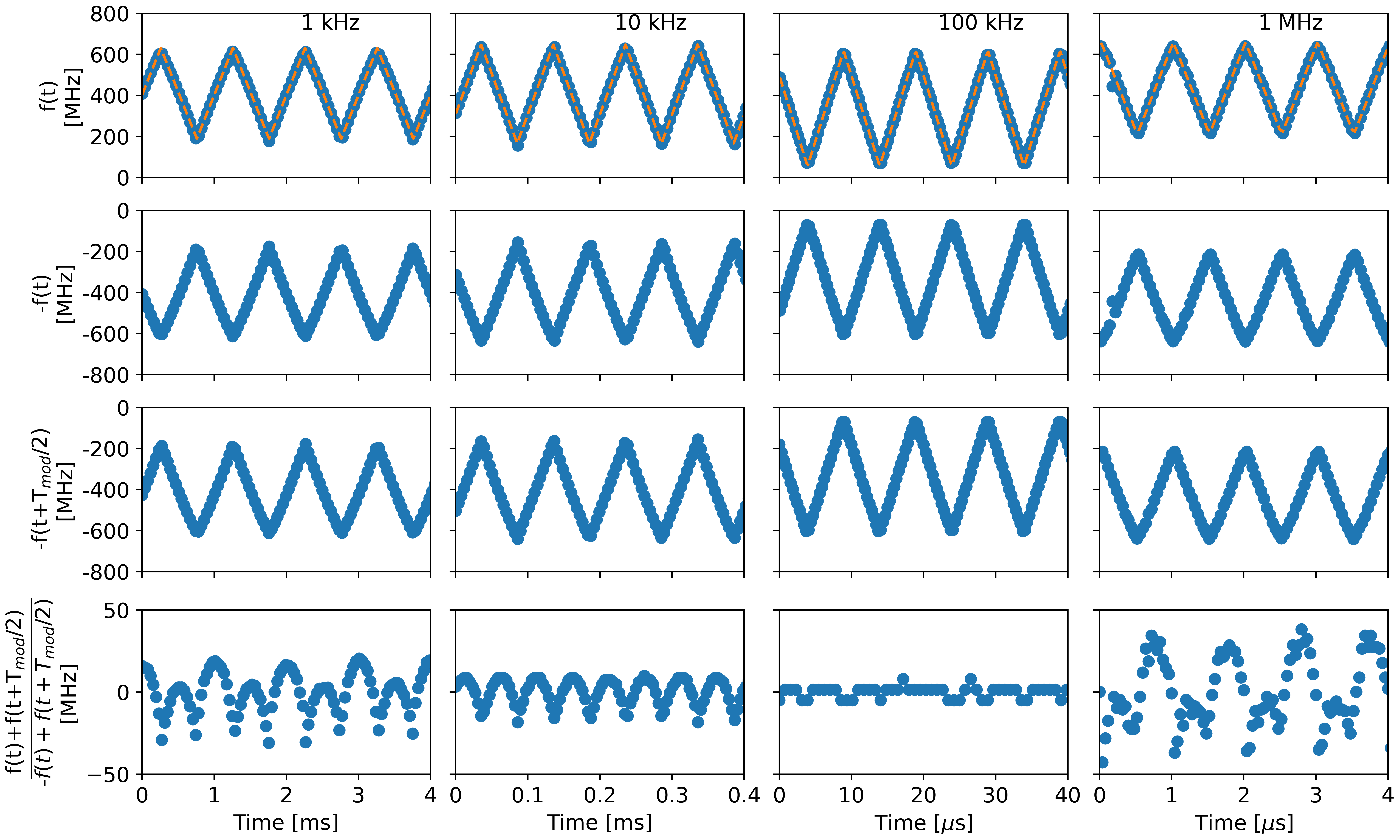
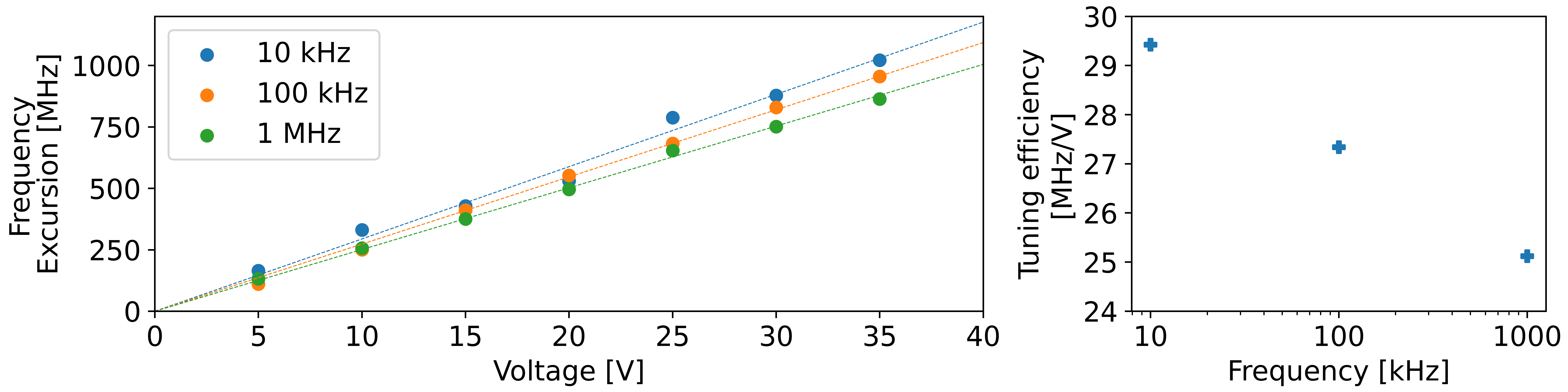
Frequency-agile laser tuning. In order to measure the voltage-to-frequency response of the LNOD microresonator, the signal from a network analyser was applied to the electrodes and the laser frequency (Toptica CTL) was fixed on the slope of the cavity resonance. This measurement reveals an important advantage of the LNOD platform: the modulation response function for the 102 GHz FSR microresonator is flat up to 100 MHz (see Fig. 3(a)). To demonstrate the frequency agility of the laser and the response of the laser frequency to a large-amplitude voltage modulation, the DFB laser was self-injection-locked to the cavity resonance and a triangular voltage signal with and modulation frequencies ranging from 1 kHz to 10 MHz was applied. No signal pre-distortion [49] or active feedback [50] were applied to the driving signal. The applied voltage modulates the refractive index of lithium niobate via the Pockels effect and shifts the cavity resonance, forcing the laser to follow the resonance as long as it remains within the overall locking range [51, 52]. To reveal the time-varying frequency-tuning characteristics for large signal modulation in the self-injection-locked state, the heterodyne beat note of the hybrid integrated laser with the reference laser was recorded on a fast photodiode. Frequency excursions remained on the level of 500 MHz, independently of the modulation frequency, whereas the nonlinearity tended to increase with increased the modulation frequency. The minimum nonlinearity of 1% of the frequency excursion is observed at a 100 kHz tuning rate. The upper row in Fig. 3(c) presents the processed laser-frequency spectrograms, which are calculated by time-segmented Fourier transformation, and the bottom row shows corresponding residuals after a perfect triangular modulation is fit to the data. Figure 3(b) shows the laser frequency excursion and the root-mean-squared deviation of the measured profiles from a perfect triangular frequency modulation determined by curve fitting. Additional data on tuning efficiency and hysteresis are shown in Supplementary Figures 3 and 4. The demonstrated frequency-modulation rate of 600 MHz in 50 ns equates to 12 PHz/s.
Although highly linear ramp frequency modulation is essential for FMCW LiDAR application [53], the frequency can be modulated in an arbitrary manner while preserving of the high tuning rate. To illustrate this, we programmed an arbitrary waveform generator to reproduce the logo of EPFL (see Fig. 3(d)) and applied the signal to the LNOD device. The laser frequency was again determined by heterodyne beat note with the reference laser, and the result of the time–frequency analysis is depicted in Fig. 3(e).
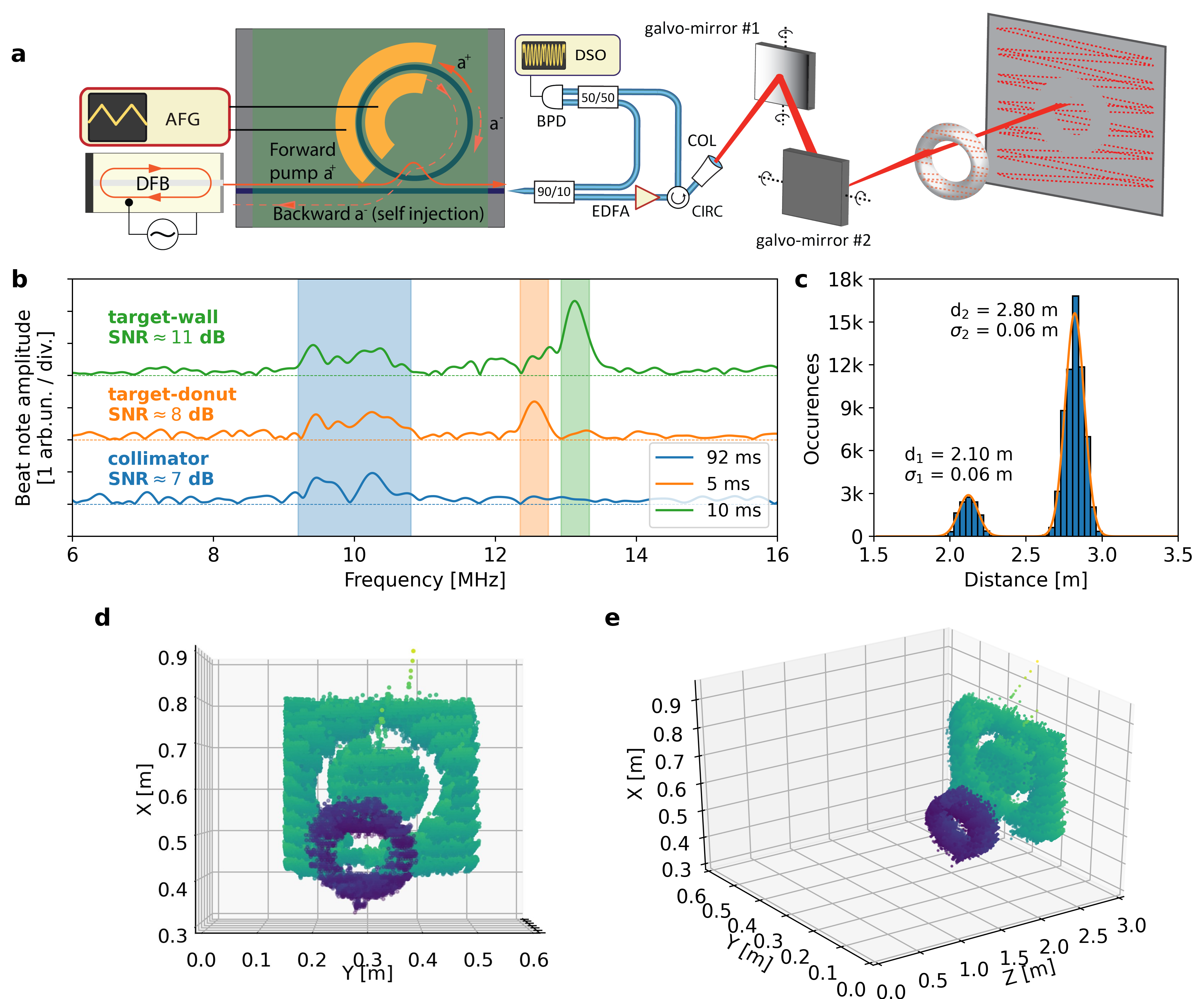
Optical coherent ranging demonstration. In order to demonstrate the application potential of our laser, we perform a proof-of-concept optical ranging experiment inside a lab environment. The FMCW LiDAR method [54] consists of a linear frequency modulation of the laser source and delayed homodyne detection with the optical signal reflected from the target. The experimental setup is depicted in Fig.4(a) (see the Methods section for a detailed description). The laser beam is scanned across the target scene by means of two galvo-mirrors with triangular driving signals. We used a polystyrene donut-like object and a metal sidewall of a rack enclosure as the target. Both objects were located approximately 3 metres away from the collimator. A photograph of the target scene and the beam-scanning pattern are depicted in Supplementary Figure 5. The beat note between the signal reflected from the target and the local oscillator is detected with a balanced photodiode and recorded by an oscilloscope. Zero-padded short-time Fourier transformation is then applied to the collected oscillogram data to retrieve the beat note spectrum evolution over 128k time slices. The time–frequency spectrograms obtained for both target and the reference Mach–Zehnder interferometer (MZI) are shown in the Supplementary Figure 6. The MZI was used for distance calibration (we retrieve the resolution of 15 cm) only and no signal pre-distortion or active feedback was applied. Figure 4(b) shows three different timeframes with beat notes of the local oscillator with the reflections from the wall, the donut and the collimator, and their respective signal-to-noise values. Last, the centre frequencies of the beat note spectra were identified and mapped into the distance domain using the MZI length as a reference. The resulting distribution of the distance values is plotted as a histogram in Fig. 4(c), showing two peaks representing the donut (at 2.1 m) and the wall (at 2.8 m). The double-Gaussian fit reveals the statistical distribution of distance values for both objects (see Fig. 4(c)). The point cloud of the 3D optical ranging is inferred from the distance data and the voltage-to-angle conversion of the galvo-mirror controller; it is shown in Fig. 4(d) and (e), where the point colour encodes the distance from the collimator.
CONCLUSION
In summary, we have demonstrated a novel heterogeneous platform for electro-optical photonic circuits using heterogeneous integration of photonic Damascene silicon nitride and thin-film lithium niobate with good fibre-to-chip coupling (3.9 dB per facet) and linear propagation losses as low as 8.5 dB/m. We have further demonstrated optical microresonators with 100 MHz loaded linewidth, wideband uniform bus–waveguide coupling and flat modulation response up to 100 MHz. Using the combination of ultra-low-loss silicon nitride photonic circuits, and endowing them with lithium niobate electro-optical modulation enables to create hybrid integrated injection locked lasers with simultaneously narrow linewidth and fast on chip tuning of 12 PHz/second. This laser source enables frequency-modulated continuous-wave optical ranging without the need for signal pre-distortion or active feedback, with a resolution of around 15 cm. With improvements in PIC design, such as a reduction of the interlayer silicon dioxide thickness and electrode-position optimization, we believe that our platform will form the basis of very fast tunable lasers with 10-ns level switching time, mode-hop-free tuning over tens of GHz, and fundamental linewidths below 100 Hz and km-level coherence length. Beyond integrated lasers, the platform can also be used to realise other devices, such as photonic switching networks for photonic computing [55] or boson sampling [56], as well as integrated transceivers that combine hybrid integrated narrow linewidth lasers with lithium-niobate-based integrated IQ-modulators. The wide transparency window of both lithium niobate [15] and silicon nitride [57, 58], moreover, allows such frequency agility to be extended to other wavelength ranges such as the mid-infrared or the visible, providing a platform for fast tunable lasers for applications ranging from optical coherence tomography [37] to trace gas sensing [59].
METHODS
Device fabrication. First, we produce a photonic Damascene silicon nitride integrated circuit. We start with a 4” silicon (Si) wafer with 4 m thermal oxide (SiO2) that we then process as follows [60]: deep-ultra-violet (DUV) stepper photolithography for preform patterning, preform dry etching, preform reflow process, low-pressure chemical vapour deposition (LPCVD) of silicon nitride (Si3N4), and chemical-mechanical polishing (CMP). An SiO2-interlayer is then deposited and subsequently polished with CMP. Prior to bonding, a few-nanometre-thick alumina layer is deposited on the donor (LNOI) and the acceptor wafer (Damascene). After that, both wafers are brought in contact and annealed for several hours at 250∘C. The silicon on the backside of the donor wafer is grinded and what is left after this step is removed with tetramethylammonium hydroxide (TMAH) wet etching. The thermal oxide is wet etched with buffered hydrofluoric acid (BHF). A layer of tungsten (W) is sputtered on the lithium niobate surface, and the electrode pattern is transferred in this layer via fluoride-based reactive ion etching (RIE). Finally, lithium niobate is etched to open the chip facets areas in order to improve the input coupling of the device on the chips by means of argon ion beam etching. The subsequent chip release is performed in three steps: dry etching of chips boundaries in silicon dioxide with fluorine-based chemistry, further etching of silicon carrier by the Bosch process, and backside wafer grinding.
Laser frequency noise measurements. We performed heterodyne beat note spectroscopy [61] beating the reference external cavity diode laser (Toptica CTL) with the hybrid integrated DFB diode laser to reveal the frequency noise of the latter. The beat note of the two signals was detected on a photodiode, and its electrical output was then sent to an electrical spectrum analyser (Rohde & Schwarz FSW43). The recorded data for the in-phase and quadrature components of the beat note were processed by Welch’s method [62] to retrieve the single sided phase noise power spectral density (PSD) that was converted to frequency noise using: . To calculate the laser linewidth, we integrate the frequency noise spectra from the intersection of the PSD with the beta-line down to the integration time of measurement [48]. The area under the curve is then recalculated to provide the full-width-half-maximum (FWHM) measure of the linewidth using: FWHM . Because a rigorous definition of the optical linewidth does depend on the integration time of the measurement we evaluate the FWHM linewidth as 56 kHz at 0.1 ms integration time, 262 kHz at 1 ms, and 1.1 MHz at 100 ms. The phase noise of the reference laser is determined by another beatnote measurement with a commercial ultrastable laser (Menlo ORS).
Thermo-refractive noise simulations. The frequency stability of the 102-GHz-FSR LNOD devices is primarily limited by the material refractive index fluctuations due to the relatively large material temperature fluctuations at resonator scale (thermo-refractive noise). To quantify the noise level in our system, we follow the approach based on the Fluctuation-Dissipation theorem (FDT), described in Ref. [63, 64, 65], that was originally given by Levin and successfully applied to the thermal noise analysis of LIGO’s mirrors. Since FDT relates fluctuations of a system to how the system dissipates energy, we simulate the noise levels with finite element method by testing how the system dissipates in response to a probe force. Since the fractional thermo-refractive noise of our device is a weighted average of the temperature fluctuations determined by the optical field distribution , in order to find out its magnitude at a particular Fourier frequency , we apply a sinusoidal entropy oscillation (energy-conjugated with temperature) at this frequency, with the same weight mimicking the field distribution, to our system in the simulation. The corresponding power dissipated in the system is retrieved from the simulation and is used to calculate the thermo-refractive noise power spectral density at this particular frequency using FDT. The device field distribution and the heat propagation simulated in the described steps are performed on COMSOL Multiphysics.
Coherent ranging experiment. The laser diode is edge-coupled to the LNOD chip with 200-nm-thick tungsten electrodes deposited along the silicon nitride waveguide on lithium niobate. The laser frequency tuning is achieved by locking the laser to a cavity resonance, fixing the DFB current, and tuning the cavity resonance via Pockels effect by a voltage applied to the electrodes. Triangular ramp signal from AWG with 0.5 Vpp amplitude and 100 kHz frequency is further amplified up to 25 Vpp by a high-voltage amplifier (Falco Systems) with 5 MHz bandwidth. No additional pre- or post- processing (linearization) was utilized for the laser frequency ramp for the coherent ranging experiment. We used the cavity resonance corresponding to 179 mA DFB current. To calibrate the frequency excursion, the 5 % fraction of the optical signal was sent to a reference Mach-Zehnder (MZI) fibre interferometer. The MZI optical length of 13.18 m was found out by an independent measurement involving a tunable diode laser scan calibrated by a frequency comb. Taking the measured MZI optical length and beatnote frequency values, the distance resolution of 15 cm is inferred. 95 % of light is split into two paths: the local oscillator path (10 %) and the target path (90 %). The signal in the target path is amplified by an EDFA (Calmar) up to 4 mW and directed to the collimator with the 8-mm aperture set to match the target distance range of 3 m. We use the galvo scanner (Thorlabs GVS112) for the beam steering. Two mirrors were controlled by linear ramp signals of 3 Hz and 60 Hz rates with the amplitude and offset values chosen to ensure that the scanning pattern fully covers the target scene. The data for the point cloud was collected within the total time interval of 1.3 s. The frame rate was limited by the galvo scanning speed and the Doppler broadening that is imparted by the rapidly tilting mirrors.
Scene reconstruction and signal data processing. The data collected in the FMCW LiDAR experiment were subject to digital signal processing steps in order to locate the scene elements in space. First, the zero-padded short-time Fourier transforms (STFT) of the beat note oscillograms from the target and the reference MZI were evaluated. The Blackman-Harris window function was used with the window size set to one period of the frequency modulated signal. Second, the obtained time-frequency maps were used to search at any given time frame the frequency values corresponding to the beat note peak. This set was filtered so that only the data points with beat note amplitudes above 1.3 were considered for further analysis. We then subtract the distance from the laser to the collimator so that the point cloud distance is given with respect to the collimator aperture position. Finally, the frequency data were converted to the distance domain, using MZI length as a reference, and the Cartesian components of each point were computed from the voltage profile applied to the galvo-mirrors.
Electro-optic S21 response measurement. A 300 W continuous wave (CW) light (1550 nm) from an external cavity diode laser (Toptica CTL) is coupled to the device using a lensed fibre. The input laser is biased at the slope of the optical resonance. A -5 dBm RF electrical signal is applied from port 1 of the network analyzer to the electrodes of the device under test, and the light intensity modulation is detected by a 12 GHz photodiode (New Focus 1544), which is sent back to port 2 of the network analyzer.
Authors Contributions: V.S. and G.L. performed experiments with the help of J.R. and A.S.. R.N.W., A.R., C.M., and J.L. developed the processes and fabricated the samples with assistance from S.H.. M.C. designed the lithography masks and performed PIC simulations. U.D., Y.P., A.R., R.N.W., and J.L. performed the CMP for bonding. D.C. performed the wafer bonding. V.S., G.L., and J.R. analysed the data. V.S. and G.H. performed thermo-refractive noise limit simulations. V.S., G.L., J.R., and T.J.K. wrote the manuscript with input from A.R., A.S., and P.S. P.S. and T.J.K. supervised the project.
Funding Information: This work was supported by Contract HR0011-20-2-0046 (NOVEL) from the Defense Advanced Research Projects Agency (DARPA), Microsystems Technology Office (MTO), and by funding from the European Union Horizon 2020 Research and Innovation Program under the Marie Sklodowska-Curie grant agreement No. 722923 (OMT) and No. 812818 (MICROCOMB), and under the FET-Proactive grant agreement No. 732894 (HOT). It was also supported by funding from the Swiss National Science Foundation under grant agreement No. 176563 (BRIDGE) and No. 186364 (QuantEOM).
Acknowledgments: The samples were fabricated in the EPFL center of MicroNanoTechnology (CMi) and the Binnig and Rohrer Nanotechnology Center (BRNC) at IBM Research. We thank the Cleanroom Operations Team of the BRNC, especially Diana Davila Pineda and Ronald Grundbacher for their help and support.
Data Availability: The code and data used to produce the plots within this work will be released on the repository Zenodo upon publication of this preprint.
References
- Zhang et al. [2017] M. Zhang, C. Wang, R. Cheng, A. Shams-Ansari, and M. Lončar, Optica 4, 1536 (2017).
- Krasnokutska et al. [2018] I. Krasnokutska, J.-L. J. Tambasco, X. Li, and A. Peruzzo, Opt. Express 26, 897 (2018).
- Wang et al. [2018] C. Wang, M. Zhang, X. Chen, M. Bertrand, A. Shams-Ansari, S. Chandrasekhar, P. Winzer, and M. Lončar, Nature 562, 101 (2018).
- He et al. [2019] M. He, M. Xu, Y. Ren, J. Jian, Z. Ruan, Y. Xu, S. Gao, S. Sun, X. Wen, L. Zhou, L. Liu, C. Guo, H. Chen, S. Yu, L. Liu, and X. Cai, Nature Photonics 13, 359 (2019).
- Zhang et al. [2019a] M. Zhang, B. Buscaino, C. Wang, A. Shams-Ansari, C. Reimer, R. Zhu, J. M. Kahn, and M. Lončar, Nature 568, 373 (2019a).
- Yang et al. [2019] Y. Yang, R. Lu, L. Gao, and S. Gong, Journal of Microelectromechanical Systems 28, 575 (2019).
- Marpaung et al. [2019] D. Marpaung, J. Yao, and J. Capmany, Nature photonics 13, 80 (2019).
- Lambert et al. [2020] N. J. Lambert, A. Rueda, F. Sedlmeir, and H. G. L. Schwefel, Advanced Quantum Technologies 3, 1900077 (2020).
- Javerzac-Galy et al. [2016] C. Javerzac-Galy, K. Plekhanov, N. R. Bernier, L. D. Toth, A. K. Feofanov, and T. J. Kippenberg, Phys. Rev. A 94, 053815 (2016).
- Ilchenko et al. [2004] V. S. Ilchenko, A. A. Savchenkov, A. B. Matsko, and L. Maleki, Phys. Rev. Lett. 92, 043903 (2004).
- Savchenkov et al. [2005] A. Savchenkov, V. Ilchenko, A. Matsko, and L. Maleki, IEEE Photonics Technology Letters 17, 136 (2005).
- Soltani et al. [2016] M. Soltani, V. Ilchenko, A. Matsko, A. Savchenkov, J. Schlafer, C. Ryan, and L. Maleki, Opt. Lett. 41, 4375 (2016).
- Dale et al. [2014] E. Dale, W. Liang, D. Eliyahu, A. A. Savchenkov, V. S. Ilchenko, A. B. Matsko, D. Seidel, and L. Maleki, in Imaging and Applied Optics 2014 (Optical Society of America, 2014) p. JTu2C.3.
- Liu et al. [2021] J. Liu, G. Huang, R. N. Wang, J. He, A. S. Raja, T. Liu, N. J. Engelsen, and T. J. Kippenberg, Nature Communications 12, 2236 (2021).
- Jhans et al. [1986] H. Jhans, J. M. Honig, and C. N. R. Rao, Journal of Physics C: Solid State Physics 19, 3649 (1986).
- Weis and Gaylord [1985] R. S. Weis and T. K. Gaylord, Applied Physics A 37, 191 (1985).
- Xiong et al. [2012] C. Xiong, W. H. P. Pernice, and H. X. Tang, Nano Letters 12, 3562 (2012).
- Wilson et al. [2020] D. J. Wilson, K. Schneider, S. Hönl, M. Anderson, Y. Baumgartner, L. Czornomaz, T. J. Kippenberg, and P. Seidler, Nature Photonics 14, 57 (2020).
- Wang et al. [2014] C. Wang, M. J. Burek, Z. Lin, H. A. Atikian, V. Venkataraman, I.-C. Huang, P. Stark, and M. Lončar, Opt. Express 22, 30924 (2014).
- Wang et al. [2015] J. Wang, F. Bo, S. Wan, W. Li, F. Gao, J. Li, G. Zhang, and J. Xu, Opt. Express 23, 23072 (2015).
- Xu et al. [2020] M. Xu, M. He, H. Zhang, J. Jian, Y. Pan, X. Liu, L. Chen, X. Meng, H. Chen, Z. Li, X. Xiao, S. Yu, S. Yu, and X. Cai, Nature Communications 11, 3911 (2020).
- Hu et al. [2020] Y. Hu, C. Reimer, A. Shams-Ansari, M. Zhang, and M. Loncar, Optica 7, 1189 (2020).
- Komljenovic et al. [2018] T. Komljenovic, D. Huang, P. Pintus, M. A. Tran, M. L. Davenport, and J. E. Bowers, Proceedings of the IEEE 106, 2246 (2018).
- Plößl and Kräuter [1999] A. Plößl and G. Kräuter, Materials Science and Engineering: R: Reports 25, 1 (1999).
- Chang et al. [2017a] L. Chang, M. H. P. Pfeiffer, N. Volet, M. Zervas, J. D. Peters, C. L. Manganelli, E. J. Stanton, Y. Li, T. J. Kippenberg, and J. E. Bowers, Opt. Lett. 42, 803 (2017a).
- Weigel et al. [2016] P. O. Weigel, M. Savanier, C. T. DeRose, A. T. Pomerene, A. L. Starbuck, A. L. Lentine, V. Stenger, and S. Mookherjea, Scientific Reports 6, 22301 (2016).
- Kondratiev et al. [2017] N. M. Kondratiev, V. E. Lobanov, A. V. Cherenkov, A. S. Voloshin, N. G. Pavlov, S. Koptyaev, and M. L. Gorodetsky, Opt. Express 25, 28167 (2017).
- Jin et al. [2021] W. Jin, Q.-F. Yang, L. Chang, B. Shen, H. Wang, M. A. Leal, L. Wu, M. Gao, A. Feshali, M. Paniccia, K. J. Vahala, and J. E. Bowers, Nature Photonics 15, 346 (2021).
- Tian et al. [2020] H. Tian, J. Liu, B. Dong, J. C. Skehan, M. Zervas, T. J. Kippenberg, and S. A. Bhave, Nature Communications 11, 3073 (2020).
- Hosseini et al. [2015] N. Hosseini, R. Dekker, M. Hoekman, M. Dekkers, J. Bos, A. Leinse, and R. Heideman, Opt. Express 23, 14018 (2015).
- Fan et al. [2016] Y. Fan, J. P. Epping, R. M. Oldenbeuving, C. G. H. Roeloffzen, M. Hoekman, R. Dekker, R. G. Heideman, P. J. M. van der Slot, and K. Boller, IEEE Photonics Journal 8, 1 (2016).
- Bostick [1967] H. Bostick, IEEE Journal of Quantum Electronics 3, 232 (1967).
- Martin et al. [2018] A. Martin, D. Dodane, L. Leviandier, D. Dolfi, A. Naughton, P. O’Brien, T. Spuessens, R. Baets, G. Lepage, P. Verheyen, P. D. Heyn, P. Absil, P. Feneyrou, and J. Bourderionnet, Journal of Lightwave Technology 36, 4640 (2018).
- Rogers et al. [2021] C. Rogers, A. Y. Piggott, D. J. Thomson, R. F. Wiser, I. E. Opris, S. A. Fortune, A. J. Compston, A. Gondarenko, F. Meng, X. Chen, G. T. Reed, and R. Nicolaescu, Nature 590, 256 (2021).
- Millot et al. [2016] G. Millot, S. Pitois, M. Yan, T. Hovhannisyan, A. Bendahmane, T. W. Hänsch, and N. Picqué, Nature Photonics 10, 27 (2016).
- Debecker et al. [2005] I. Debecker, A. K. Mohamed, and D. Romanini, Opt. Express 13, 2906 (2005).
- Ji et al. [2019] X. Ji, X. Yao, Y. Gan, A. Mohanty, M. A. Tadayon, C. P. Hendon, and M. Lipson, APL Photonics 4, 090803 (2019).
- Churaev et al. [2021] M. Churaev, A. Riedhauser, R. N. Wang, M. A. Anderson, C. Möhl, V. Snigirev, T. Blésin, A. Siddharth, Y. Popoff, D. Caimi, S. Hönl, J. Riemensberger, J. Liu, P. Seidler, and T. J. Kippenberg, in review (2021).
- Karpov et al. [2016] M. Karpov, H. Guo, A. Kordts, V. Brasch, M. H. P. Pfeiffer, M. Zervas, M. Geiselmann, and T. J. Kippenberg, Phys. Rev. Lett. 116, 103902 (2016).
- Gyger et al. [2020] F. Gyger, J. Liu, F. Yang, J. He, A. S. Raja, R. N. Wang, S. A. Bhave, T. J. Kippenberg, and L. Thévenaz, Phys. Rev. Lett. 124, 013902 (2020).
- Brasch et al. [2014] V. Brasch, Q.-F. Chen, S. Schiller, and T. J. Kippenberg, Opt. Express 22, 30786 (2014).
- Komljenovic et al. [2016] T. Komljenovic, M. Davenport, J. Hulme, A. Y. Liu, C. T. Santis, A. Spott, S. Srinivasan, E. J. Stanton, C. Zhang, and J. E. Bowers, Journal of Lightwave Technology 34, 20 (2016).
- Chang et al. [2017b] L. Chang, M. H. P. Pfeiffer, N. Volet, M. Zervas, J. D. Peters, C. L. Manganelli, E. J. Stanton, Y. Li, T. J. Kippenberg, and J. E. Bowers, Opt. Lett. 42, 803 (2017b).
- Pfeiffer et al. [2018a] M. H. P. Pfeiffer, C. Herkommer, J. Liu, T. Morais, M. Zervas, M. Geiselmann, and T. J. Kippenberg, IEEE Journal of Selected Topics in Quantum Electronics 24, 1 (2018a).
- Pfeiffer et al. [2018b] M. H. P. Pfeiffer, J. Liu, A. S. Raja, T. Morais, B. Ghadiani, and T. J. Kippenberg, Optica 5, 884 (2018b).
- Gorodetsky et al. [2000] M. L. Gorodetsky, A. D. Pryamikov, and V. S. Ilchenko, JOSA B 17, 1051 (2000).
- Henry [1982] C. Henry, IEEE Journal of Quantum Electronics 18, 259 (1982).
- Domenico et al. [2010] G. D. Domenico, S. Schilt, and P. Thomann, Appl. Opt. 49, 4801 (2010).
- Zhang et al. [2019b] X. Zhang, J. Pouls, and M. C. Wu, Opt. Express 27, 9965 (2019b).
- Roos et al. [2009] P. A. Roos, R. R. Reibel, T. Berg, B. Kaylor, Z. W. Barber, and W. R. Babbitt, Opt. Lett. 34, 3692 (2009).
- Ilchenko et al. [2011] V. S. Ilchenko, E. Dale, W. Liang, J. Byrd, D. Eliyahu, A. A. Savchenkov, A. B. Matsko, D. Seidel, and L. Maleki, in Laser Resonators and Beam Control XIII, Vol. 7913, edited by A. V. Kudryashov, A. H. Paxton, and V. S. Ilchenko, International Society for Optics and Photonics (SPIE, 2011) pp. 295 – 303.
- Lihachev et al. [2021] G. Lihachev, J. Riemensberger, W. Weng, J. Liu, H. Tian, A. Siddharth, V. Snigirev, R. N. Wang, J. He, S. A. Bhave, and T. J. Kippenberg, Ultralow-noise frequency-agile photonic integrated lasers (2021), arXiv:2104.02990 [physics.optics] .
- Uttam and Culshaw [1985] D. Uttam and B. Culshaw, Journal of Lightwave Technology 3, 971 (1985).
- Behroozpour et al. [2017] B. Behroozpour, P. A. M. Sandborn, M. C. Wu, and B. E. Boser, IEEE Communications Magazine 55, 135 (2017).
- Drake et al. [1986] B. L. Drake, R. P. Bocker, M. E. Lasher, R. H. Patterson, and W. J. Miceli, Optical Engineering 25, 38 (1986).
- B. et al. [2013] S. J. B., M. B. J., H. P. C., K. W. Steven, J. Xian-Min, B. Marco, D. Animesh, T.-P. Nicholas, L. N. K., K. Dmytro, G. J. C., S. B. J., S. P. G. R., and W. I. A., Science 339, 798 (2013).
- Morin et al. [2021] T. J. Morin, L. Chang, W. Jin, C. Li, J. Guo, H. Park, M. A. Tran, T. Komljenovic, and J. E. Bowers, Optica 8, 755 (2021).
- Guo et al. [2018] H. Guo, C. Herkommer, A. Billat, D. Grassani, C. Zhang, M. H. P. Pfeiffer, W. Weng, C.-S. Brès, and T. J. Kippenberg, Nature Photonics 12, 330 (2018).
- Truong et al. [2013] G.-W. Truong, K. O. Douglass, S. E. Maxwell, R. D. van Zee, D. F. Plusquellic, J. T. Hodges, and D. A. Long, Nature Photonics 7, 532 (2013).
- Pfeiffer et al. [2018c] M. H. P. Pfeiffer, C. Herkommer, J. Liu, T. Morais, M. Zervas, M. Geiselmann, and T. J. Kippenberg, IEEE Journal of Selected Topics in Quantum Electronics 24, 1 (2018c).
- Duthel et al. [2009] T. Duthel, G. Clarici, C. R. S. Fludger, J. C. Geyer, C. Schulien, and S. Wiese, IEEE Photonics Technology Letters 21, 1568 (2009).
- Welch [1967] P. Welch, IEEE Transactions on Audio and Electroacoustics 15, 70 (1967).
- Levin [1998] Y. Levin, Phys. Rev. D 57, 659 (1998).
- Kondratiev and Gorodetsky [2018] N. Kondratiev and M. Gorodetsky, Physics Letters A 382, 2265 (2018).
- Huang et al. [2019] G. Huang, E. Lucas, J. Liu, A. S. Raja, G. Lihachev, M. L. Gorodetsky, N. J. Engelsen, and T. J. Kippenberg, Phys. Rev. A 99, 061801 (2019).
Supplementary Information to:
Ultrafast tunable lasers using lithium niobate integrated photonics
Viacheslav Snigirev1,∗, Annina Riedhauser2,∗, Grigory Lihachev1,∗, Johann Riemensberger1, Rui Ning Wang1, Charles Möhl2, Anat Siddharth1, Guanhao Huang1, Youri Popoff2,3, Ute Drechsler2, Daniele Caimi2, Simon Hönl2, Junqiu Liu1, Paul Seidler2, and Tobias J. Kippenberg1
1 Institute of Physics, Swiss Federal Institute of Technology Lausanne (EPFL), CH-1015 Lausanne, Switzerland
2 IBM Research Europe, Zurich, Säumerstrasse 4, CH-8803 Rüschlikon, Switzerland
3 Integrated Systems Laboratory, Swiss Federal Institute of Technology Zürich (ETH Zürich), CH-8092 Zürich, Switzerland
∗ These authors contributed equally to this work