Nils Meyer
Grid on QPACE 4
Abstract
In 2020 we deployed QPACE 4, which features 64 Fujitsu A64FX model FX700 processors interconnected by InfiniBand EDR. QPACE 4 runs an open-source software stack. For Lattice QCD simulations we ported the Grid LQCD framework to support the ARM Scalable Vector Extension (SVE). In this contribution we discuss our SVE port of Grid, the status of SVE compilers and the performance of Grid. We also present the benefits of an alternative data layout of complex numbers for the Domain Wall operator.
1 Introduction
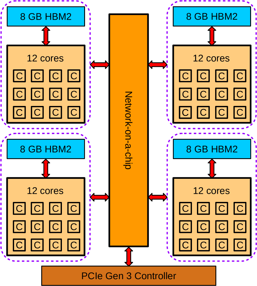
Lattice QCD has traditionally been a developer and early adopter of new high-performance computing (HPC) resources. A very promising new instruction set architecture is Arm’s Scalable Vector Extension (SVE), which has been implemented in hardware for the first time in the A64FX processor developed by RIKEN R-CCS and Fujitsu. This processor powers Japan’s flagship Fugaku supercomputer and is also used in the QPACE 4 cluster at the University of Regensburg.
Porting and optimizing Lattice QCD code for a new hardware architecture has been a difficult and time-consuming task in the past. The Grid Lattice QCD framework [1] makes this task much easier by isolating the details of the hardware in a few files at the lowest layer of the software stack. Our port of Grid to SVE is described in [2, 3, 4]. In this contribution we study the performance of this port on QPACE 4, including compiler performance and a different choice of the data layout for complex numbers compared to Grid.
2 QPACE 4
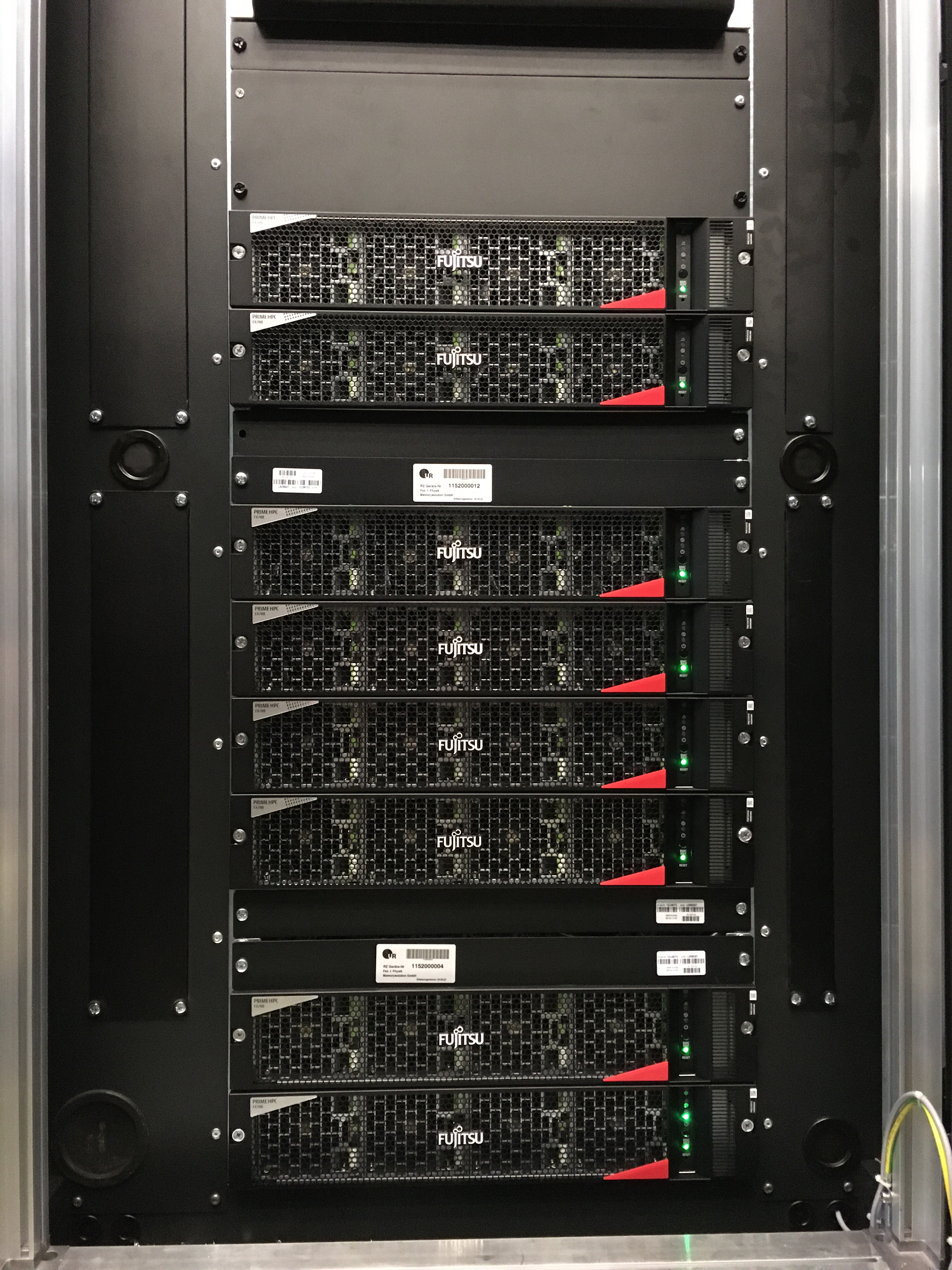
QPACE 4 is the latest member of the QCD PArallel Computing Engine (QPACE) series. The small-scale cluster features compute nodes from the Fujitsu PRIMEHPC FX700 series. QPACE 4 was deployed at the University of Regensburg in June 2020 and is shown in Fig. 2. The key characteristics of QPACE 4 are
-
•
64 Fujitsu A64FX CPUs, 48 cores each (up to 4 NUMA domains), 1.8 GHz (see Fig. 2)
-
•
512-bit ARM Scalable Vector Extension (SVE)
-
•
177/354 TFlop/s peak in double/single precision (DP/SP)
-
•
2048 GB HBM2 memory total
-
•
InfiniBand EDR interconnect (100 Gbit/s)
We run an open-source software stack using CentOS Stream 8, GCC 10.1 and OpenMPI 4.0. For storage we use the GlusterFS parallel file system. For Lattice QCD we use Grid [1] and the Grid Python Toolkit (GPT) [5].
3 Main memory throughput
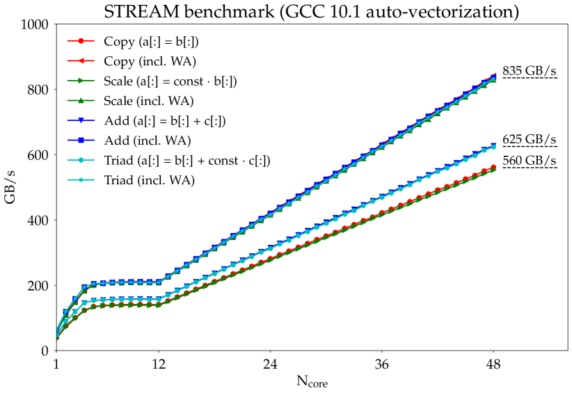
The nominal aggregate peak throughput of the HBM2 memories of a single node is 1 TB/s. The de-facto standard benchmark for evaluation of memory throughput is the STREAM benchmark [6]. STREAM consists of four mini-benchmarks (copy, scale, add, and triad). The mini-benchmarks differ in computation and in the load/store ratio of array elements. For copy and scale the load/store ratio is 1:1 per element, and for add and triad this ratio is 2:1.
We show thread scaling of the STREAM benchmark on a single QPACE 4 node in Fig. 4. Data throughput scales with the number of cores in use if . We measure up to 625 GB/s of benchmark data throughput. The caches of the A64FX implement a write-back policy, i.e., a cache block is loaded from main memory on a write miss. This is called Write Allocation (WA). WA causes extra data traffic and thus reduces the effective memory throughput. Including WA traffic, the data throughput is up to 835 GB/s. We note that STREAM on a single Fugaku node (48 compute cores, 2.2 GHz) yields comparable results despite the difference in clock frequencies.
4 Grid on QPACE 4
4.1 Port to A64FX (512-bit SVE)
The ARM C Language Extensions (ACLE) provide access to SVE vector types and SVE instructions in C/C++ [7]. We use ACLE to implement Grid’s lower-level functions. Grid stores complex numbers in memory alternating real and imaginary parts (see Fig. 5). We refer to this layout as RIRI. We use hardware support for processing complex numbers. We published the details of the implementation in [2, 3, 4]. Our Grid port to the A64FX is available in upstream Grid (configure --enable-simd=A64FX).
Key computational kernels such as Wilson Dslash and the performance-relevant part of the Domain Wall operator, which we refer to as Domain Wall kernel and discuss in detail in [8], are specialized to the A64FX using ACLE and the RIRI layout. Manual instruction scheduling facilitates instruction latency hiding and optimal use of the register file. We use software prefetching to optimize the data flow between compute cores and memory hierarchy. Specialized kernels are enabled by the command line argument --dslash-asm when starting binaries.

4.2 Benchmarks
Grid features a rich set of tests and performance benchmarks. Here we present a relevant subset of benchmarks to illustrate the performance of Grid on QPACE 4.
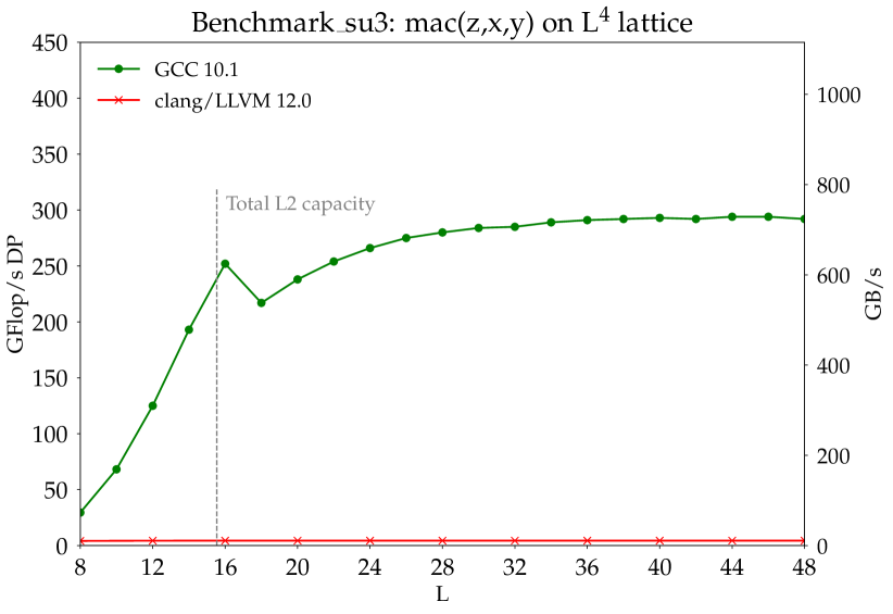
Benchmark_su3 performs independent SU(3) matrix multiplication on each lattice site in a 4d volume. This benchmark is well suited for SVE compiler testing. We show the performance of SU(3) matrix multiplication as a function of the lattice volume on a single QPACE 4 node in Fig. 4. Using GCC 10.1 we achieve up to about 300 GFlop/s DP, which corresponds to a benchmark data throughput of about 744 GB/s not taking into account WA traffic. We also show the performance of the open source LLVM/clang SVE compiler. LLVM/clang-based SVE compilers (including open source LLVM/clang, Arm’s armclang, and also Fujitsu’s compiler in clang mode) introduce unnecessary copy operations and therefore generate non-optimal code. We did not test Cray’s LLVM/clang-based SVE compiler, but we expect similar results. At present we recommend using GCC 10.1 or 10.2.
| Volume | 1 MPI rank | 4 MPI ranks | ||
|---|---|---|---|---|
| DP | SP | DP | SP | |
| 360 | 893 | 321 | 619 | |
| 350 | 990 | 383 | 827 | |
| 339 | 1023 | 383 | 898 | |
| Volume | 1 MPI rank | 4 MPI ranks | ||
|---|---|---|---|---|
| DP | SP | DP | SP | |
| 484 | 949 | 408 | 803 | |
| 477 | 958 | 409 | 815 | |
| 476 | 960 | 432 | 875 | |
The performance of the Wilson Dslash kernel and the Domain Wall kernel is shown in Table 1 and 2, respectively, on a single QPACE 4 node. We observe a mild performance penalty using 4 MPI ranks compared to 1 MPI rank. We attribute this penalty to the overhead associated with inter-process communication using shared memory. SP performance is nominally expected to be about twice the DP performance due to the doubling of the Flop throughput. We observe this for the Domain Wall kernel, while for the Wilson Dslash kernel DP performance is lower than expected. To explain this, we note that (a) Grid uses different data layouts for SP and DP and (b) the Domain Wall kernel has higher cache reuse than the Wilson Dslash kernel. Performance variations for different lattice volumes are mild. We attribute the variations to the details of cache reuse, which differ amongst lattice volumes. We note that GCC 10.1 and 10.2 deliver best performance. LLVM/clang-based compilers and other versions of GCC perform worse.
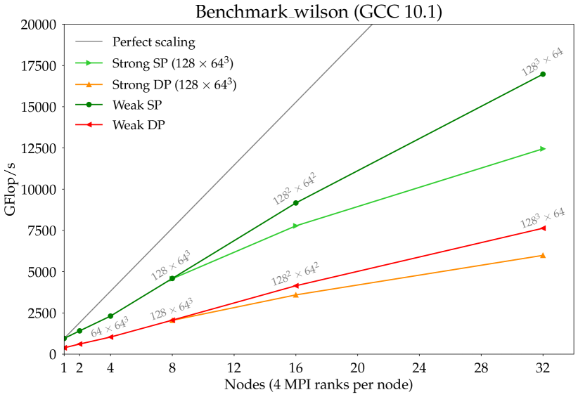
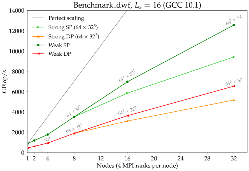
The multi-node performance of key computational kernels using MPI is shown in Figs. 7 and 7. QPACE 4 has two separate InfiniBand partitions, and the maximum number of nodes within each partition is 32. Grid’s MPI code path is non-trivial. For instance, it includes many branches in the instruction stream, multiple function calls, irregular memory access, and communication over the network. We observe a significant performance drop running on multiple nodes compared to a single node despite large local volumes. Differences between 1 rank per node and 4 ranks per node are marginal (< 3%). Further investigation is necessary to identify and resolve bottlenecks in the MPI code path.
4.3 Alternative layout of complex numbers
Grid only supports the RIRI layout for complex numbers. In a collaboration with University of Erlangen we studied the Domain Wall kernel using an alternative data layout for complex numbers on Fugaku [8]. We illustrate the RRII layout in Fig. 5. Key characteristics of the RIRI and RRII layout are shown in Table 3. For RIRI we use the svcadd () and svcmla () intrinsics for processing complex numbers (). The corresponding instructions have high latencies and limitations on pipeline usage (see [8, 9] for details). SVE does not support complex multiplication without addition of a third operand. For RRII only real arithmetics is necessary, which comes with lower instruction latencies and no limitations on pipeline usage.
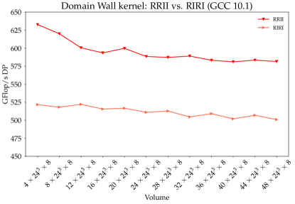
We tested the RRII layout on the A64FX extending GridBench [10], which features a subset of Grid. We implemented the Domain Wall kernel using ACLE and used datasets generated by Grid. GridBench does not support MPI, therefore benchmarks are restricted to a single node. On Fugaku (48 cores, 2.2 GHz) the RRII layout outperforms RIRI by up to 12% [8]. On a single QPACE 4 node the RRII layout outperforms RIRI by up to about 20%, see Fig. 8. Instructions processing complex numbers predominantly use the FLA pipeline, thereby leading to imbalanced pipeline usage. Pipeline usage is balanced using real arithmetics, which is the case for the RRII layout. RIRI consumes up to 20% more energy than RRII on Fugaku. RRII energy consumption benefits further from shutting down one of the two floating-point pipelines with minor impact on performance. Currently we are not able to shut down pipelines on QPACE 4 due to missing software support. However, we expect energy savings comparable to, or even higher than, Fugaku and comparable impact on performance. We plan to extend Grid to support the RRII layout in the future.
| RIRI | RRII | |
| Parallel lattice site updates | 4 DP, 8 SP | 8 DP, 16 SP |
| Full spinor projection to half spinor | svcadd () if applicable | Real arithmetics |
| Reconstruction of full spinor | svcadd () if applicable | Real arithmetics |
| SU(3) half spinor | svcmla () | Real arithmetics |
| Real Flop per lattice site update | 1416 (need to compute ) | 1320 |
| FLA / FLB pipeline usage | Imbalanced | Balanced |
5 Summary and outlook
QPACE 4 comprises 64 Fujitsu A64FX CPUs interconnected by InfiniBand EDR. The A64FX achieves outstanding performance for Lattice QCD applications. GCC 10.1 and 10.2 achieve best overall performance, while other compilers underperform. An alternative layout of complex numbers is beneficial on the A64FX, but has yet to be integrated into Grid. The necessary code modifications remain future work.
Acknowledgment
We acknowledge funding of the QPACE 4 project provided by the Deutsche Forschungsgemeinschaft (DFG) in the framework of SFB/TRR-55. Furthermore, we acknowledge support from the HPC tools team at Arm. We thank Yasumichi Aoki, Peter Boyle, Issaku Kanamori, and Yoshifumi Nakamura for valuable discussions.
References
- [1] P. Boyle, A. Yamaguchi, G. Cossu and A. Portelli, Grid: A next generation data parallel C++ QCD library, PoS (LATTICE 2015) (2016) 023 [1512.03487]
- [2] N. Meyer, P. Georg, D. Pleiter, S. Solbrig and T. Wettig, SVE-enabling Lattice QCD Codes, 2018 IEEE International Conference on Cluster Computing (CLUSTER) (2019) 623 [1901.07294]
- [3] N. Meyer, D. Pleiter, S. Solbrig and T. Wettig, Lattice QCD on upcoming Arm architectures, PoS (LATTICE 2018) (2019) 316 [1904.03927]
- [4] N. Meyer, D. Pleiter, S. Solbrig and T. Wettig, Lattice QCD on QPACE 4, 2020 Asian-Pacific Symposium of Lattice Field Theory (APLAT 2020)
- [5] C. Lehner et al., Grid Python Toolkit (GPT), [https://github.com/lehner/gpt]
- [6] J. D. McCalpin, Memory Bandwidth and Machine Balance in Current High Performance Computers, IEEE Computer Society Technical Committee on Computer Architecture (TCCA) (1995)
- [7] Arm, ARM C Language Extensions for SVE, [https://developer.arm.com/documentation/100987/latest/]
- [8] C. Alappat, N. Meyer, J. Laukemann, T. Gruber, G. Hager, G. Wellein and T. Wettig, Execution-Cache-Memory modeling and performance tuning of sparse matrix-vector multiplication and Lattice quantum chromodynamics on A64FX, Concurrency and Computation Pract. Exper. (2021) e6512
- [9] Fujitsu, A64FX Microarchitecture Manual, [https://github.com/fujitsu/A64FX/tree/master/doc]
- [10] N. Meyer and C. Alappat, GridBench with A64FX support, [https://github.com/nmeyer-ur/GridBench/tree/intrinsics]