Fabry-Perot interferometer with quantum well mirror for controllable dispersion compensation
Abstract
In this work we propose a controllable dispersion compensation mirror based on Fabry-Perot interferometer with quantum well. The choice of the parameters of the heterostructure and experiment geometry makes it possible to introduce negative dispersion in narrow spectral region with maintaining the constant reflection coefficient. Feasibility of this concept is proved experimentally by measurements of the reflectivity form InGaAs/GaAs quantum well. The control of quantum well exciton parameters could be used to switch the dispersion compensation on and off.
Dispersion control plays important role both in optical communication systems [1] and in short-pulsed lasers [2, 3]. In most cases, it is necessary to introduce negative (anomalous) dispersion, since optical materials have normal dispersion in their transparency region (, where – refractive index of the medium, and – light frequency). In many applications Fabry-Perot interferometer (FPI)-based reflectors are used to introduce the negative group delay dispersion (GDD), expressed as , where is the optical phase.
The Fabry-Perot interferometer [4] is an optical cavity formed by two parallel mirrors. The complex reflection coefficient of such resonator could be expressed as follows:
| (1) |
where and are complex reflection coefficients of mirrors and is the phase build up after the round-trip of the light in the cavity.
Chromatic dispersion compensation can be done without adding losses by a Gires-Tournois interferometer (GTI) [5], which is a FPI with the highly reflective second mirror (). The reflectivity for the GTI is close to unity at any wavelength, but the phase of reflected light depends on the light frequency in a periodic manner. The GTI has spectral region, where it may introduce fixed negative GDD without the possibility to control its value except for the complex and unstable variable-gap GTIs.
Saturable absorber semiconductor mirror (SESAM) is the GTI with the saturable absorber introduced into the gap between mirrors. SESAM could be used to introduce different negative GDD values depending on the incident light intensity. Usually the epitaxially grown quantum well (QW) is used as the absorber. Such active mirrors could be used for modelocking and short pulse generation in lasers [6, 7, 8, 9].
In this work we propose a new active mirror structure – an FPI with the QW acting as one of the mirrors. Careful design of the structure and the excitation geometry leads to wavelength-independent reflectivity with the negative GDD introduced near the QW exciton resonance. Such FPI is similar to the GTI, but allows one to switch the GDD to zero by the bleaching of the exciton resonance (for example, by additional control pulse). We consider this active mirror theoretically and demonstrate the feasibility of its design by the measurements of the reflectivity of the heterostructure with an InGaAs/GaAs QW.
1 Theory
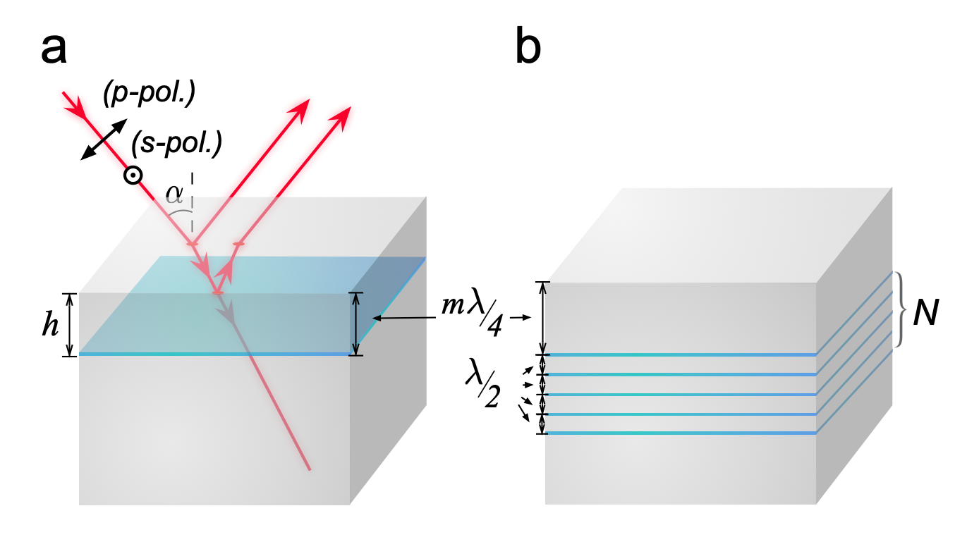
Let us consider a heterostructure shown in Figure 1(a) consisting of a substrate, a thin QW layer, and a cap layer with thickness . The refractive index of the semi-infinite substrate and the cap layer is , and the air refractive index is . In this case the FPI is formed between the surface and the QW layer. Let us denote the amplitude reflection coefficient for structure/air interface as (real number), and the QW layer amplitude reflection coefficient as (complex number). The reflectivity of the structure could be found as and for the FPI (Eq. (1)) could be represented in the following form:
| (2) |
In the case of a thin single QW the reflection coefficient could be represented in the following way [10]:
| (3) |
where is the exciton resonance radiative width, – its non-radiative broadening, and – detuning of the exciton resonance frequency from the light frequency .
The proposed FPI structure should have the constant reflectivity across the whole spectral range. In what follows, this situation will be referred to as compensation mode. Away from the exciton resonance, tends to the non-resonant Frensel reflectivity . Thus, to maintain the spectral uniformity, it is necessary for the second term in the expression (2) to be equal to zero across the whole spectral range, which can be achieved when the following condition is met (taking into account Eq. (3)):
| (4) |
This condition could be satisfied for any only if . Thus, the necessary criterion for the constant reflectivity is , where . Note that this is valid only for sufficiently small , when the phase can be considered weakly dependent on the wavelength. Taking this criterion into account, Eq. (4) could be solved leading to the condition , where the compensation reflection coefficient is the following:
| (5) |
where is a quality factor. Consider that . For ideal QW () , and for realistic QW structures .
For a given QW cap layer thickness (determined by ) and quality factor the compensation mode can always be found for certain light polarization and incident angle. Compensation conditions are summarized in Table 1, where – reflection coefficient for structure/air interface at normal incidence, – Brewster’s angle.
| Quality factor | Angle of incidence | Polarization | |
|---|---|---|---|
| even | – | p | |
| odd | p | ||
| odd | p, s | ||
| odd | s |
Note that at and odd the compensation takes place at normal incidence (), and thus does not depend on the polarization of the incident light. The angle of incidence at which the compensation occurs can be found as follows:
| (6) |
where , and for p- and s-polarizations correspondingly. The dependency is summarized in Fig. 2, a.
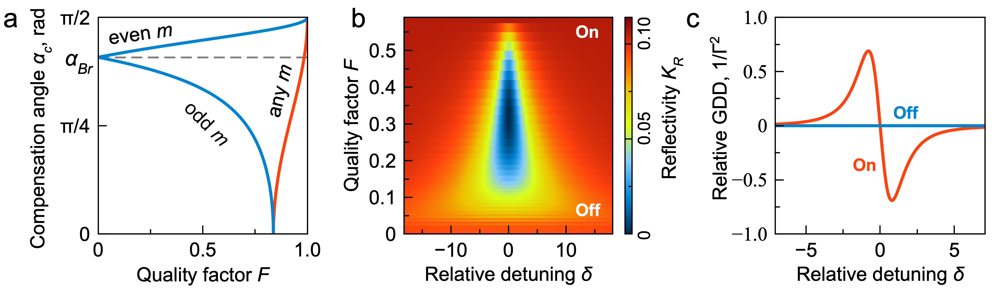
The compensation at normal incidence, which is particularly interesting for practical applications, imposes rather strong requirements on the QW quality. For example, in the case of GaAs/vacuum interface (, ) the quality factor for the normal compensation should be , what is beyond the capabilities of current QWs growth methods. This requirement can be relaxed if the multiple QW (MQW) structure is used instead of the single QW (Fig. 1(b)). The MQW structure consists from QWs separated by layers so that the reflection from these QWs interferes constructively [10]. If all the QWs have approximately the same and values then all previous calculations remains the same except for the replacement of the single QW quality factor with effective quality factor , where is the quality factor of single QW in the MQW. In this case even for the low-quality QWs the compensation at normal incidence still could be observed for proper MQW structure. It should be noted that is also achievable for MQW structures. In this situation, compensation becomes impossible.
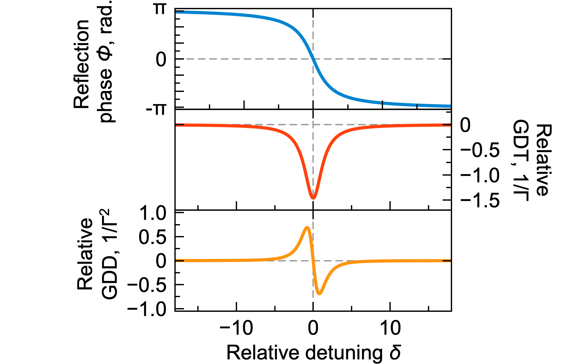
The reflection phase could be calculated as . For the structure with the reflection phase could be represented in the following way for the compensation condition in the vicinity of the resonance frequency :
| (7) |
| (8) |
where is the relative detuning and .
The group delay time (GDT) could be calculated in relative units of by differentiating of the reflection phase with respect to the relative detuning :
| (9) |
The GDT is always negative. One more derivation leads to the group delay dispersion (GDD) in relative units of :
| (10) |
Figure 3 shows phase, GDT and GDD values for (same as in the QW structure studied in experimental section).
The main advantage of proposed QW-based mirror is the ability to turn on and off the dispersion compensation by the external stimulus. Fast bleaching of the QW resonance by control laser beam could lead to the switching of to almost zero value. This could be done by the rapid increase of due to excitons scattering on quasiparticles introduced by the control light pulse [11, 12, 13, 14, 15]. Figure 2(b) shows the reflectivity spectra for different values. The compensation in the ”on” state takes place at with the constant and non-zero GDD (Fig. 2(c), red curve). The mirror could be switched to the ”off” state by the rapid decrease of to zero. In this case the reflectivity remains the same as in the ”on” state, but the GDD vanishes (Fig. 2(c), blue curve).
2 Experiment
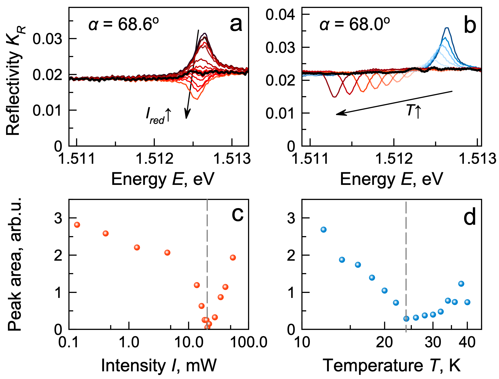
To demonstrate the compensation mode, we used molecular beam epitaxy to grow the sample P553 on a (100) GaAs substrate with a 2 nm In0.02Ga0.98As/GaAs QW and 295 nm GaAs cap layer. Such layer roughly correspond to thickness (). The sample was grown without rotation, which allows us to exactly satisfy the compensation condition for by choosing a specific point on the sample.
The sample was kept in a closed-loop helium cryostat. The reflectivity spectrum was measured using the white lamp focused down to 100 m spot and a spectrometer with a CCD detector. The QW heavy-hole exciton resonance was observed at eV at 10 K. The sample could be illuminated by a 656 nm cw laser in order to introduce additional broadening of the exciton resonance.
The required cap layer thickness was found by the reflectivity observation. Once the thickness is a product of the exciton feature in reflectivity became symmetric. Further, the compensation conditions could be met by the choice of the angle of incidence . However, the angle-tuning experiment is challenging. Therefore, we fixed and p-polarization (the condition in the second row of Table 1). The further fine tuning of the compensation conditions was made by the variation. Since of the exciton resonance is fixed for the QW composition and thickness [16] the quality factor can be varied by tuning of . Non-radiative broadening includes all possible broadening sources. The inhomogeneous broadening is determined by the sample, so it could not be varied. The homogeneous broadening includes thermal broadening due to the exciton-phonon interaction, and all additional sources of the irreversible phase relaxation, such as exciton scattering on charge carriers, excitons and other elementary excitations. In this work, we used two methods for fine tuning of by increase of the homogeneous broadening: illumination of the sample above the QW barrier and sample heating.
Figure 4(a) shows the acquired reflectivity of the sample at 10 K for different intensities of the additional 656 nm illumination up to 100 mW measured before the lens that focuses light onto the sample. Illumination excites quasiparticles, which introduce additional homogeneous broadening and decrease . In the absence of illumination, constructive interference of signals reflected from the QW and the sample surface is observed. With an increase in the illumination intensity , the amplitude of the interference decreases, and at a certain illumination intensity, the compensation is observed – the reflectivity ceases to depend on the wavelength (black curve in the figure). With a further growth of the interference changes to the destructive one. Figure 4(c) shows the dependency of the area under the interference peak (area between experimental curve and non-resonant reflectivity level) with the growth of . At mW this area turns to zero manifesting the compensation.
Similar experiment was carried out for the temperature rise (Fig. 4(b)). An increase in temperature leads to an increase in broadening, but in this case, a red shift of the exciton resonance frequency is also observed. At K the minimum of the interference peak is reached (see Fig. 4(d)) and the compensation condition is met.
The calculation for the parameters of the experimentally studied single QW shows that the compensation is observed at , the maximum GDT is expected to be around -10 ps and maximum absolute value of GDD around 10 ps/nm.
3 Conclusion
In this work, we suggested the possibility of controlled dispersion compensation using a Fabry-Perot interferometer with a QW as a mirror. In the experiment with a single InGaAs/GaAs QW, we demonstrated the sample layout and experimental geometry, in which there is no reflection feature associated with exciton resonance. The reflectivity remains constant, and theoretical calculations predict the presence of a nonzero GDD near the exciton resonance. This GDD could be switched off by the external stimulus without change of the reflectivity.
Further steps towards the practical application of the proposed structure could be done. MQW can be used to achieve the compensation for normal incidence and larger GDD value. The overall reflectance of the system can be made higher than the Fresnel reflectance of the material and closer to unity by using QWs as the surface mirror and a distributed Bragg reflector as the bottom one. Finally, the proposed effect can also be demonstrated at room temperature using materials with higher exciton binding energies, such as GaN.
4 Funding
This work was funded by Russian Foundation for Basic Research with grant 20-32-70163.
5 Acknowledgments
The experimental study was carried out using the equipment of Saint Petersburg State University (SPbU) resource center “Nanophotonics”.
References
- [1] S. Orfanidis, Electromagnetic Waves and Antennas (Sophocles J. Orfanidis, 2016).
- [2] P. M. W. French, G. F. Chen, and W. Sibbett, \JournalTitleOptics Communications 57, 263 (1986).
- [3] W. Sibbett, Ultrashort pulses for nonlinear optical techniques (Springer Netherlands, Dordrecht, 1993), pp. 363–414.
- [4] C. Fabry and A. Perot, \JournalTitleAnn. Chim. Phys. 16, 115–144 (1899).
- [5] F. Gires and T. P., \JournalTitleC. R. Acad. Sci. 258, 6112–6115 (1964).
- [6] U. Keller, K. Weingarten, F. Kartner, D. Kopf, B. Braun, I. Jung, R. Fluck, C. Honninger, N. Matuschek, and J. Aus der Au, \JournalTitleIEEE Journal of Selected Topics in Quantum Electronics 2, 435 (1996).
- [7] A. Isomäki, A. Vainionpää, J. Lyytikäinen, and O. G. Okhotnikov, \JournalTitleAppl. Phys. Lett. 82, 2773 (2003).
- [8] A. Isomäki, M. Rusu, L. Orsila, M. Guina, and O. Okhotnikov, \JournalTitlePhysica Scripta 114, 145 (2004).
- [9] M. Moenster, U. Griebner, W. Richter, and G. Steinmeyer, \JournalTitleIEEE Journal of Quantum Electronics 43, 174 (2007).
- [10] E. Ivchenko, Optical Spectroscopy of Semiconductor Nanostructures (Alpha Science, 2005).
- [11] P. Y. Shapochkin, S. Eliseev, V. Lovtcius, Y. P. Efimov, P. Grigoryev, E. Khramtsov, and I. Ignatiev, \JournalTitlePhys. Rev. Applied 12, 034034 (2019).
- [12] P. Y. Shapochkin, M. S. Lozhkin, I. A. Solovev, Y. P. Efimov, S. Eliseev, V. Lovtcius, and Y. V. Kapitonov, \JournalTitleAppl. Phys. Lett. 116, 081102 (2019).
- [13] A. S. Kurdyubov, B. F. Gribakin, A. V. Mikhailov, A. V. Trifonov, Y. P. Efimov, S. A. Eliseev, V. A. Lovtcius, and I. V. Ignatiev, \JournalTitleSemiconductors 54, 1514 (2020).
- [14] A. S. Kurdyubov, A. V. Trifonov, I. Y. Gerlovin, B. F. Gribakin, P. S. Grigoryev, A. V. Mikhailov, I. V. Ignatiev, Y. P. Efimov, S. A. Eliseev, V. A. Lovtcius, M. Aßmann, M. Bayer, and A. V. Kavokin, \JournalTitlePhys. Rev. B 104, 035414 (2021).
- [15] B. F. Gribakin, E. S. Khramtsov, A. V. Trifonov, and I. V. Ignatiev, \JournalTitlePhys. Rev. B 104, 205302 (2021).
- [16] S. Poltavtsev, Y. Efimov, Y. Dolgikh, S. Eliseev, V. Petrov, and V. Ovsyankin, \JournalTitleSolid State Communications 199, 47 (2014).