Electron dynamics in a 2D nanobubble:
A two-level system based on spatial density
Abstract
Nanobubbles formed in monolayers of transition metal dichalcogenides (TMDCs) on top of a substrate feature localized potentials, in which electrons can be captured. We show that the captured electronic density can exhibit a non-trivial spatiotemporal dynamics, whose movements can be mapped to states in a two-level system illustrated as points of an electronic Poincaré sphere. These states can be fully controlled, i.e, initialized and switched, by multiple electronic wave packets. Our results could be the foundation for novel implementations of quantum circuits.
I Introduction
Monolayers of transition metal dichalcogenides (TMDCs) are atomically thin two-dimensional (2D) semiconductors attractive for several applications in electronics and optoelectronics.[1, 2, 3, 4] Due to their two-dimensional nature and the strong dependence of the material properties on strain and substrates, TMDC monolayers can host localized potentials of different extensions, ranging from few Angstroms for atomic defects [5, 6, 7, 8] to several hundreds of nanometers for strain-induced potentials.[9, 10, 11, 12, 13] They are receiving increasing interest in the context of quantum information processing, because localized excitons may serve as single photon sources [9]. Localized potentials can be either deterministically induced, for example by patterned substrates [14, 10, 11, 12, 13] and helium irradiation,[7] or they build up naturally in the form of defects and disorder [5, 6, 8] or nanobubbles.[15, 16, 17, 18, 19, 20, 21, 22, 23] Bubbles are naturally formed in experiments when depositing the 2D material on a substrate,[16, 17, 19, 21, 22, 23, 24] similar to the everyday process of air-bubbles forming when putting a plastic foil on glass. Bubbles in various monolayers and of different dimensions can also be obtained via bottom-up approaches such as ionic irradiations. [24, 25] Nanobubbles are able to induce an energy confinement due to the interplay of strain and local screening variations,[15] resulting in a non-trivial circular shape recently observed in experiments.[22, 23] Besides being extensively studied via optical response,[14, 10, 11, 12, 13, 26, 27, 28] localized potentials can impact also the transport and associated recombination in different hosting 2D materials [29, 30, 8] and even lead to excitonic funneling for larger potentials.[31, 32, 33, 34, 35]
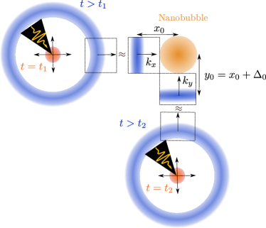
In localized structures a non-trivial spatiotemporal dynamics can be induced by capture from an electronic wave packet moving in the 2D monolayer.[36] In particular the carrier capture can be mediated by the emission of phonons, which interact strongly with the electrons in the TMDC monolayer.[37, 38] The crucial property behind this peculiar dynamics is the locality of the carrier capture process, which was already studied in quantum wire-dot geometries.[39, 40, 41] In this paper we combine two state-of-the art theoretical approaches to describe the dynamics of electronic wave packets in a realistic model of a TMDC hosting a nanobubble. We show that the resulting dynamics of the captured distribution can be well controlled by a combination of impinging wave packets, Fig. 1(a), allowing movements ranging from linear along varying axes to circular. We show that all movements can be initialized, switched and mapped on a Poincaré sphere, analogous to the polarization states of light. This means that the electronic movement of the captured density inside the nanobubble can be understood as a two-level system, which could be used as quasi-stationary quantum state.
II System set-up
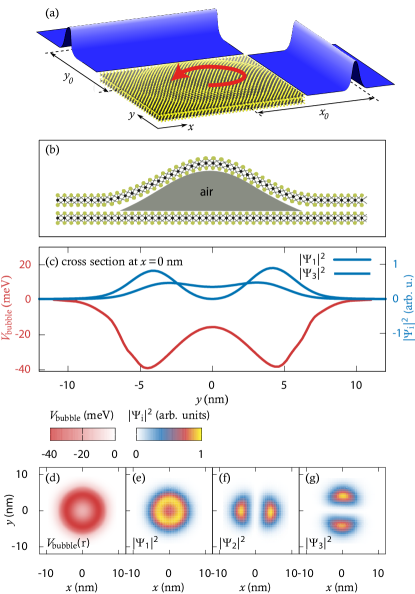
A sketch of our system is shown in Fig. 1(a): In a TMDC monolayer a nanobubble (yellow-gray area) is formed. To calculate the potential created by this nanobubble, we utilize microscopic calculations, based on atomic force field and subsequent tight-binding simulations (see also Supporting Information). The method is based on the requirements of covering strain as well as local changes of the screening and electronic hybridization on the nanometer scale. To investigate the interplay between TMDC layer deformations and carrier confinement, we model a TMDC layer encapsulating an air bubble with atomic resolution using a million-atom supercell as shown in Fig. 1(b) similar to Ref. [15]. Considering as a material a MoS2 monolayer, the effects of the nanobubble result in the formation of a zero-dimensional (0D) confinement potential in the conduction band as plotted in Figs. 1(c) and (d): It is mostly radially symmetric and shows the values of maximum depth (about -40 meV) distributed on a ring, rather than at the center. This is the result of two different spatially-varying contributions, i.e. dielectric constant and strain, which are stronger at the center and tail of the nanobubble, respectively.[15] This non-trivial shape has been recently experimentally observed in TMDC-based structures[22, 23] via photoluminescence studies. Note that for bubbles with higher aspect ratios the shape is more triangular.[15]
We then insert the microscopically obtained 0D potential in the Schrödinger equation using for electrons in K valley standard single-particle dispersion [42, 43] and scalar plane-waves approximation.[36] Besides the (quasi-)continuous states with positive energies we find 5 bound states at the energies meV, meV and meV and meV. The wave functions of the and states are plotted in Figs. 1(e-g) and additionally a cross section along the line nm of the and one state is shown together with the potential in Fig. 1(c). One can see a slight tilt of the states with respect to the and axis and also a slight asymmetry of with respect to due to small deviations from radial symmetry [cf. Figs. 1(c,g)].
These states now act as a basis for the density matrix treatment to describe the dynamics of the electronic density in the 2D-0D TMDC system. Mimicking a strongly-localized optical excitation, we construct an electronic wave packet as initial condition. While different amplitudes and orientations will be used, in the following all wave packets have the same excess energy as well as energetic and spatial width (see Supporting Information for additional information). The excess energy of meV corresponds to a velocity of nm/ps (for a possible experimental realization see Supporting Information).
We then set up the equation of motion for the density matrix including the carrier-phonon interaction. In particular, here we account for the electron-phonon interaction with longitudinal optical (LO) phonons of energy meV via the Fröhlich coupling.[44, 37] We use a Lindblad formalism [36] including all non-diagonal density matrix elements accounting for the spatial inhomogenity in our system [45], capturing most effects found also in quantum kinetics calculations (for more details see Refs. [39, 41, 36, 46] and Supporting Information). We note that for the traveling wave packet we consider coherent dynamics in contrast to diffusion dynamics already observed in experiments.[47, 48, 49, 50, 51, 30, 8, 52] Here in fact we address the dynamics in the very first few hundreds of femtoseconds at very low temperature, where TMDCs show scattering times of several picoseconds [53] and energy-thermalization timescales of tens of picoseconds, as recently experimentally observed for related excitons [54] via phonon-assisted photoluminescence, cf. [55]. The slow intravalley thermalization observed at low temperatures is due to the decreased effectiveness of scattering with phonons, as observed optically via vanishing associated contribution to the excitonic linewidth.[56, 57, 58, 59] For these reasons we restrict ourselves to the coherent limit for the traveling distribution, while due to energy separations the capture is typically ruled by emission of optical phonons,[39, 40, 60, 41] as also shown recently for excitons in Mo-based TMDC monolayers.[46] Since we discuss the capture of electrons, we focus on the Fröhlich coupling which is particularly efficient in these materials.[37] We stress that we focus on the low-density regime, so that Pauli-blocking or Coulomb-induced effects [61] can be neglected.
When the wave packets impinge on the nanobubble, carriers are captured into the bound states via the electron-phonon interaction. Previous studies have shown that besides energy selection rules, the carrier capture crucially depends on the spatial characteristics, as it can happen only when the wave packet is in the vicinity of the nanobubble, i.e. the capture is local,[39, 41, 36] and it is affected by its direction of motion.[36] More details on the methods and simulation can be found in the Supporting Information and in Refs. [15] and [36].
III Dynamics at the bubble
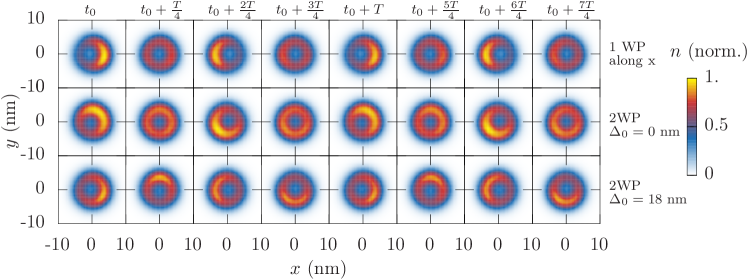
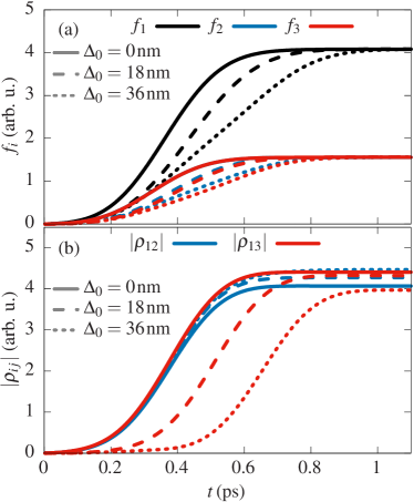
During passage of the wave packets, electrons with a density of are captured into the nanobubble.[36] Figure 2 shows snapshots of the captured density for different scenarios. The time takes into account that the wave packet needs a certain time to reach the nanobubble where it can be captured. Using a typical starting distance nm, the time is given by 350 fs (cf. also Fig. S2 in Supporting Information) and analogous for .
In Fig. 2(top row) the effect of a single wave packet moving along the -direction and crossing the nanobubble is shown. The captured electronic density displays an oscillatory movement along the -axis. The oscillation results from the capture into a superposition state of the localized p-states and the s-state. Therefore the period agrees well with the value provided by the energy difference between and state, i.e. ps. For a different potential, a similar movement was discussed in Ref. [36]. In the following, we use two wave packets of the same amplitude: one traveling along and one traveling along (see Fig. 1(a)). The dynamics of the density inside the nanobubble is controlled by adjusting the initial distance of the two wave packets from the nanobubble. We define the difference in starting distances as . Note that other control scenarios are also possible, e.g., by changing the respective starting time. A spatial separation corresponds to a temporal separation between the moment in which the corresponding wave packets impinge on the nanobubble. Thereby, nm marks the distance corresponding to the travel of a wave packet during a period . Figure 2(middle row) shows the captured density from two wave packets with , i.e., . The density oscillates in a diagonal movement between the upper right and lower left corner. Using a finite difference nm corresponding to a time we can induce a anti-clockwise circular movement, shown in Fig. 2(bottom row). We stress that such a movement cannot be induced by a single wave packet alone.
To quantify these movements, we define the center-of-mass (COM) as
and analogously for . The evolution of the COM for different is shown in Fig. 3, where the color encodes the increasing time.
Depending on the number of wave packets and their starting distance , we obtain different types of movement: For a single wave packet along , the COM-movement is just along as shown in Fig. 3(a), while : This happens because the initial configuration is symmetric along , and such a symmetry is preserved by the captured density only if the latter has no oscillations in [36]. Note that the residual slight deviation from strictly null value of can be traced back to the slight asymmetry of the wave function in Figs. 1(c,g). Obviously, it is possible to induce a vertical oscillation in a completely analogous manner by excitation along the -axis. This is shown in Fig. 3(b).
For the cases shown in the middle and lower row of Fig. 2, two wave packets with nm and nm, respectively, we find a diagonal movement in Fig. 3(c) and a circular movement in Fig. 3(e). If we now increase the starting difference further, for nm we find an anti-diagonal movement in Fig. 3(d) and for nm a left-circular movement in Fig. 3(f). These distances correspond to time shifts of multiples of , namely, , , and for (c), (e), (d) and (f), respectively. For separations of that are not a multiple of an elliptical movement is obtained.
IV Electronic motion as a two-level system
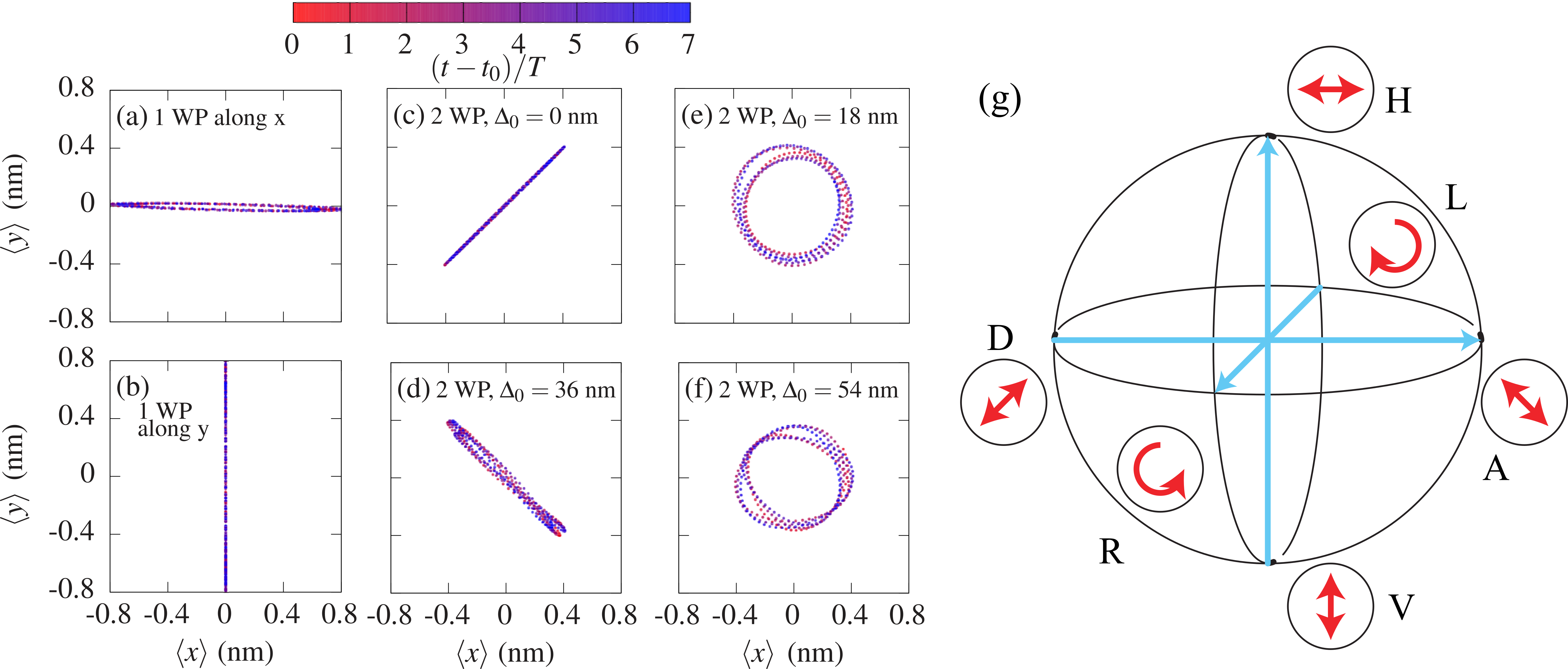
Modern quantum technologies rely on properly-defined Poincaré spheres e.g. as defined via the different light polarizations.[62, 63] As sketched in Fig. 3(g), a Poincaré sphere displays horizontal and vertical polarizations on the poles ( and ) while showing on the equator diagonal/anti-diagonal ( and ) as well as left- and right-circular polarizations ( and ). Remarkably, these points resemble the electronic COM found in Fig. 3 (cf. red arrows in Fig. 3(g) with Figs. 3(a-f)). Starting with these empirical considerations, we exploit the above-discussed density dynamics to introduce an electronic Poincaré sphere analogous to the one defined e.g. by light polarization.
Considering that only the and two states contribute to the dynamics within the nanobubble, the spatial density in the nanobubble can be separated into three parts
| (1) |
where is the contribution not displaying any dynamics after the capture is completed. and are the electronic motions in the horizontal and vertical direction, which can be written as
| (2) |
with the spatial profiles and time shift and the frequency (see Supporting Information for more details). Note that we can map the spatial profiles by using the occupations and coherences of the eigenstates in the nanobubble potentials as outlined in Supporting Information.
If we consider two equally shaped wave packets impinging from and direction, the central factor for the electronic motion within the nanobubble are the times when they impinge on the nanobubble. The time difference introduces a phase difference between the horizontal and vertical oscillation according to Eq. (2), which determines the movement achieved in the nanobubble.
From Eqs. (1) and (2) we can extract the COM-movement to
| (3) | |||||
normalized to the total captured density
We here used that .
The two-dimensional vector in Eq. (3) can be written as
with and denoting the real part. The vector is an electronic analog of the Jones vector,[63] which is one of the possible ways for describing the light polarization. Another option to describe the polarization of light is the Stokes vector.[62, 63] Also for the Stokes vector we can introduce the electronic spatial analog using
| (4) |
From the four Stokes parameters one can define the electronic Poincaré sphere with squared radius as sketched in Fig. 3(g). From the electronic Poincaré sphere we can define the generic state of the electronic oscillation as [63]
| (5) |
with
| (6) |
where . Equation (5) is a formal way to associate a quantum-mechanical state on the electronic Poincaré sphere with the real oscillations of the captured electronic density. The density oscillations can thereby be unambiguously mapped onto a Poincaré sphere considering the amplitudes and and the phase difference .
The Jones vector, Stokes coefficients and electronic Poincaré sphere are all analogous ways to describe a two-level system of the electronic spatial oscillations inside the nanobubble, with e.g. being the ground state and the excited one. Of course different choices of basis states are possible.[63] We stress that the electronic state in Eq. (5) per se is time independent, as the Jones vector, Stokes coefficient and Poincaré-sphere points do not depend on time , but only depend on time shifts and . Nevertheless, its manifestation are time-dependent oscillations of or, analogously, of . Such an electronic two-level system could be useful e.g. to store information in a stationary qubit.
V State switching
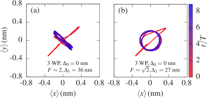
The proposed mechanisms can go beyond the initialization of the electronic Poincaré sphere by switching its state. To show this we start initializing a diagonal movement with . Then we add a third wave packet traveling along the -direction, which is shifted w.r.t. the first one by and has an amplitude bigger by a factor than the amplitude of the first two.
The dynamics of the COM for the electronic density captured inside the TMDC nanobubble is shown in Fig. 4. In both cases it starts with the diagonal movement induced by the first two wave packets (red dots between first and third quadrant in Figs. 4(a,b)). In the first control example of Fig. 4(a) the third wave packet has twice the intensity of the first two () and starts with nm. As a result, the initial diagonal movement is switched into the anti-diagonal one (blue dots between second and fourth quadrant). The simulation results are consistent with previous considerations: While the first two wave packets induce a state , the third one induces an additional contribution . Note that we do not use normalized states here because in the end the state must be normalized to the total density present in the system (thereby defining the radius of the Poincaré sphere). The first two wave packets are initialized with in and direction and the second one with in -direction, such that the sum thus provides . We then have
Note that the overall amplitude of the COM has decreased by approximately a factor of 2 w.r.t. to the initial state due to the normalization mentioned above, cf. Eq. (3) and Fig. 4(a).
In the second example we set and nm, corresponding to an additional phase of the third wave packet w.r.t. the first two. The result is shown in Fig. 4(b), which shows a right-circular motion. The state is expected, because besides state we can calculate in the vertical direction . Even more versatile controls can be obtained by adding additional wave packets. This shows that the wave packets can fully control the electronic Poincaré sphere via both initialization and switch, indicating the versatility of the proposed two-level system.
VI Conclusion
In conclusion, we have demonstrated an electronic Poincaré sphere, whose states can be initialized and switched by capture from traveling wave packets. For this purpose we combine the first-principle description of a TMDC nanobubble and associated confining potential with a density-matrix description of ultrafast electronic transport and capture. Thanks to the locality of the carrier capture the non-trivial dynamics of the captured distribution can be fully controlled. We find that the phase difference between horizontal and vertical oscillation is analogous to the polarization states of light, i.e. the Poincaré sphere, and fully controllable by the time delay of additional wave packets. Our results show how new opportunities of information protocols could be offered by the miniaturization properties of two-dimensional materials and the spatial control of carrier dynamics.
Acknowledgements
We thank F. A. Reiter for graphical help with Fig. 1. R. R. acknowledges funding from the Deutsche Forschungsgemeinschaft (DFG) through SFB 1083 (subproject B9) and the European Union’s Horizon 2020 research and innovation programme under grant agreement no. 881603 (Graphene Flagship). F. L. and D. E. R. acknowledge financial support by the Deutsche Forschungsgemeinschaft (DFG) through the project 406251889 (RE 4183/2-1). C. C., M. F., F. J., and M. L. acknowledge support by the Deutsche Forschungsgemeinschaft (DFG) within RTG 2247 and through a grant for CPU time at the HLRN (Göttingen/Berlin).
Appendix A Simulation details
Our simulation is a multi-step process: (i) We perform a microscopic calculation of the nanobubble potential based on a combination of valence force field and 6-band tight binding model. (ii) The nanobubble potential is inserted into the Schrödinger equation for K-valley electrons, yielding bound and free states together with the corresponding energies. (iii) Using the wave functions obtained from the Schrödinger equation as basis states, we set up the equation of motion for the electron density matrix in the framework of a Lindblad superoperator technique. (iv) As initial condition we construct wave packets in the subspace of the free states localized at a certain distance from the nanobubble and calculate their time evolution according to the density matrix equation. We here describe these steps in detail:
Regarding step (i): For the simulation of the nanobubble we use a combination of atomic force field calculations with tight binding simulations. Starting from a paraboloid profile of the nanobubble, the atoms in the upper TMDC layer are relaxed, while the atoms in the lower layer are kept fixed. This part of the simulation is performed using a REAX potential [64] with the parametrization from Ref. [65] within a valence force field calculation, which is capable of accurately describing bond deformations under strain as well as continuous bond formation and breaking dynamics. Based on these valence force field simulations, new equilibrium positions of the individual atoms in the bended material are determined. Information about the displaced atoms is used in a subsequent tight-binding electronic-state calculation for the supercell structure. For a supercell with an in-plane extension of 130 nm and up to 1.2 atoms, a 6-band tight-binding Hamiltonian is solved as discussed in Ref. [15]. Strain-induced local band gap changes arising from the displaced atomic positions are included via a generalized Harrison rule [66].
Additionally, when locally detaching the upper layer from the substrate underneath and changing from a commensurate bilayer to monolayer-like structures across the nanobubble, the upper layer is subject to a modified dielectric environment and electronic hybridization is hence different than in a bilayer [67, 68, 69, 70]. As discussed in Ref. [15], these effects are included in the calculation by changing individual tight-binding parameters.
Regarding step (ii): We insert the potential evaluated in step (i) in a Schrödinger equation where we assume that the eigenstates for the bare-monolayer behave around the K valley as scalar plane waves with free eigenenergies [36], with Å, 1.66 eV, eV, =75 meV and meV [42, 43], cf. also Ref. [36].
Regarding step (iii): We further set up the equations of motion taking into account the free evolution of the electronic wave packet (see point (iv) below for its initial definition) and scattering with LO phonon via Fröhlich interaction. While for excitons intervalley scattering can be very important [56, 55, 54, 52], despite efficient Hamiltonian coefficients [38] free electrons close to the K-valley energy mininum cannot directly scatter in the free states of other valleys due to energy conservation or uneffectiveness of absorption of phonons with finite energies at cryogenic temperatures. In view of the picoseconds scattering times [53] and tens of picoseconds energy-thermalization time of related excitonic states [54], intravalley scattering with acoustic phonon of K electrons is expected to take place at longer timescales than the ones here considered, hence it is neglected. As a consequence we restrict ourselves to the free coherent evolution for the free distribution. The scattering between free and bound states is dominated by optical phonon modes due to energy separation between emitting and receiving states[39, 40, 41], as shown recently for excitons in Mo-based TMDC monolayers [46]. In particular here we focus on the effective scattering with LO phonon via Fröhlich interaction, whose scattering coefficients between electronic states in valley K with momenta are given by , where the electron-LO phonon Hamiltonian follows Ref. [37]. These scattering coefficients have been inserted in a Lindblad approach for the carrier capture [41, 36], which is able to describe the scattering from the delocalized states into the localized ones not only tracking the energy of the emitting states, but also the spatial information. Key to describe the dynamics in this highly inhomogeneous case is the off-diagonal nature of the Lindblad superoperator together with an energetic broadening of the energy conservation, the latter previously included by comparison with the full quantum kinetics calculations [41], although more recent studies have shown similar broadenings [46].
Finally, regarding point (iv) we choose a wave-front type packet, which in the density matrix and in the basis of the free TMDC states and for the -propagating case can be written as [36]
where is the 2D wave vector and is the Heaviside step function. The wave packet propagating along has the same form with and (). The wave packets have a finite width in space and energy of = 10 nm and = 5 meV, respectively, and are centered at or () for propagation along and , respectively. The excess energy, which determines the velocity as well as the bound states which are energetically favorable for the carrier capture, is taken to be meV, i.e., an energy close to ELO, with and being the energy of state 1 and nearly degenerate states 2 and 3, respectively (see main manuscript). Such a wave packet can in principle be found in certain distances from the excitation spot of a strongly localized near-field source [36]. The energetic width meV corresponds then to an ultrafast excitation of about 150 fs duration. These length and timescales could be combined as typically done in the field of ultrafast nano-optics (see, e.g., [71] for a review on experimental applications). These experimental developments have led to extensive studies of nanometric wave packets (see, e.g., [72, 73, 74]). A specific setup for the presented system is given in Fig. S5, where two near-field sources lead to the considered wave packets in and direction impinging on the nanobubble. In this setup a temporal delay between the exciting pulses can be used to effectively tune the difference in starting positions .
Note that we work in the single-band approximation with the standard single-particle dispersion [42, 43], while also excitonic effects in TMDC monolayers are very prominent [3, 4]. Nevertheless beside the formation of deeply-bound excitons [75, 76], in competition with spatial separation between electrons and holes [61], we also expect electronic wave packets able to travel through the monolayer and then be captured in the here-considered ultrafast timescale.
Appendix B Occupations and coherences of the captured electrons
While in the manuscript we focus purely on the description using the real-valued density, it is interesting to consider the occupation and the coherences of the bound states. More details on the quantum mechanical description of the states using the density matrix formalism can be found in previous publications [45, 39, 40, 77, 41, 36].
In the density matrix formalism the single particle density matrix within the eigenbasis states is given by
from which the spatial distribution is calculated via
In our case the states correspond to the bound states in the nanobubble potential (see discussion in the main text). Since for our initial conditions the the occupation of the states and is negligible, we will restrict our discussion to states .
The occupations and coherences of the states are then given respectively by
The most remarkable feature is that the capture from the 2D system into the 0D localized potential results not only in occupations, but in a superposition state of the different states [36]. The general density matrix reads
| (7) |
with and H.c. denoting the Hermitian conjugate, and where we introduced in the interaction picture. This equation already shows that the capture into the superposition state results in a dynamics of the captured density with the frequency . The shape of the dynamics, however, is determined by the magnitude of the occupations together with the absolute values of the coherences and and most importantly the relative time difference between the coherences, which in turn is determined by the time of the carrier capture.
One example of carrier capture dynamics is shown in Fig. S6, where the dynamics of (a) the occupations and (b) the coherences is shown. We stress again that the capture happens locally, i.e., when the wave packet is close to the nanobubble as can be seen in the corresponding finite rise time of the occupations [41]. The final capture is slightly stronger into state then into the excited states and as seen in Fig. S6(a), while the coherences after the capture in Fig. S6(b) are equally strong. However, the build-up of the population and in particular the coherences is different: The wave packet traveling along the -direction induces the coherence , while the wave packet traveling along -direction induces . When the latter wave packet is delayed, builds up later, but the final value is almost independent of . One may therefore approximate the dynamics of as with the Heaviside function when approximating the build-up of coherence as instantaneous at the arrival time of the wavepacket in -direction. Accordingly we find for these three examples the diagonal movement, the circular movement and the anti-diagonal movement due to the phase difference .
From the microscopic picture given in Eq. (7) we obtain the spatial profiles of the oscillation of the density as defined in Eq. (2) of the main manuscript. In particular we find that and with the starting distance from the QD and replacing we get similar expressions for and . This connects the quantum mechanical picture of the states on the Poincaré sphere to the dynamics of the captured density.
References
- Wang et al. [2012] Q. H. Wang, K. Kalantar-Zadeh, A. Kis, J. N. Coleman, and M. S. Strano, Electronics and optoelectronics of two-dimensional transition metal dichalcogenides, Nat. Nanotechnol. 7, 699 (2012).
- Mak and Shan [2016] K. F. Mak and J. Shan, Photonics and optoelectronics of 2D semiconductor transition metal dichalcogenides, Nat. Photonics 10, 216 (2016).
- Wang et al. [2018] G. Wang, A. Chernikov, M. M. Glazov, T. F. Heinz, X. Marie, T. Amand, and B. Urbaszek, Colloquium: Excitons in atomically thin transition metal dichalcogenides, Rev. Mod. Phys. 90, 021001 (2018).
- Mueller and Malic [2018] T. Mueller and E. Malic, Exciton physics and device application of two-dimensional transition metal dichalcogenide semiconductors, npj 2D Mater. Appl. 2, 29 (2018).
- Zhou et al. [2013] W. Zhou, X. Zou, S. Najmaei, Z. Liu, Y. Shi, J. Kong, J. Lou, P. M. Ajayan, B. I. Yakobson, and J.-C. Idrobo, Intrinsic structural defects in monolayer molybdenum disulfide, Nano Lett. 13, 2615 (2013).
- Zhang et al. [2017] S. Zhang, C.-G. Wang, M.-Y. Li, D. Huang, L.-J. Li, W. Ji, and S. Wu, Defect structure of localized excitons in a monolayer, Phys. Rev. Lett. 119, 046101 (2017).
- Klein et al. [2019] J. Klein, M. Lorke, M. Florian, F. Sigger, L. Sigl, S. Rey, J. Wierzbowski, J. Cerne, K. Müller, E. Mitterreiter, P. Zimmermann, T. Taniguchi, K. Watanabe, U. Wurstbauer, M. Kaniber, M. Knap, R. Schmidt, J. J. Finley, and A. W. Holleitner, Site-selectively generated photon emitters in monolayer MoS2 via local helium ion irradiation, Nat. Commun. 10, 2755 (2019).
- Chu et al. [2020] Z. Chu, C.-Y. Wang, J. Quan, C. Zhang, C. Lei, A. Han, X. Ma, H.-L. Tang, D. Abeysinghe, M. Staab, X. Zhang, A. H. MacDonald, V. Tung, X. Li, C.-K. Shih, and K. Lai, Unveiling defect-mediated carrier dynamics in monolayer semiconductors by spatiotemporal microwave imaging, Proc. Natl. Acad. Sci. 117, 13908 (2020), https://www.pnas.org/content/117/25/13908.full.pdf .
- Tonndorf et al. [2015] P. Tonndorf, R. Schmidt, R. Schneider, J. Kern, M. Buscema, G. A. Steele, A. Castellanos-Gomez, H. S. J. van der Zant, S. M. de Vasconcellos, and R. Bratschitsch, Single-photon emission from localized excitons in an atomically thin semiconductor, Optica 2, 347 (2015).
- Kern et al. [2016] J. Kern, I. Niehues, P. Tonndorf, R. Schmidt, D. Wigger, R. Schneider, T. Stiehm, S. Michaelis de Vasconcellos, D. E. Reiter, T. Kuhn, and R. Bratschitsch, Nanoscale positioning of single-photon emitters in atomically thin WSe2, Adv. Mater. 28, 7101 (2016).
- Branny et al. [2017] A. Branny, S. Kumar, R. Proux, and B. D. Gerardot, Deterministic strain-induced arrays of quantum emitters in a two-dimensional semiconductor, Nat. Commun. 8, 15053 (2017).
- Palacios-Berraquero et al. [2017] C. Palacios-Berraquero, D. M. Kara, A. R.-P. Montblanch, M. Barbone, P. Latawiec, D. Yoon, A. K. Ott, M. Loncar, A. C. Ferrari, and M. Atatüre, Large-scale quantum-emitter arrays in atomically thin semiconductors, Nat. Commun. 8, 15093 (2017).
- Rosenberger et al. [2019] M. R. Rosenberger, C. K. Dass, H.-J. Chuang, S. V. Sivaram, K. M. McCreary, J. R. Hendrickson, and B. T. Jonker, Quantum calligraphy: Writing single-photon emitters in a two-dimensional materials platform, ACS Nano 13, 904 (2019).
- Kumar et al. [2015] S. Kumar, A. Kaczmarczyk, and B. D. Gerardot, Strain-induced spatial and spectral isolation of quantum emitters in mono- and bilayer WSe2, Nano Lett. 15, 7567 (2015).
- Carmesin et al. [2019] C. Carmesin, M. Lorke, M. Florian, D. Erben, A. Schulz, T. O. Wehling, and F. Jahnke, Quantum-dot-like states in molybdenum disulfide nanostructures due to the interplay of local surface wrinkling, strain, and dielectric confinement, Nano Lett. 19, 3182 (2019).
- Khestanova et al. [2016] E. Khestanova, F. Guinea, L. Fumagalli, A. K. Geim, and I. V. Grigorieva, Universal shape and pressure inside bubbles appearing in van der Waals heterostructures, Nat. Commun. 7, 12587 (2016).
- Shepard et al. [2017] G. D. Shepard, O. A. Ajayi, X. Li, X.-Y. Zhu, J. Hone, and S. Strauf, Nanobubble induced formation of quantum emitters in monolayer semiconductors, 2D Mater. 4, 021019 (2017).
- Chirolli et al. [2019] L. Chirolli, E. Prada, F. Guinea, R. Roldán, and P. San-Jose, Strain-induced bound states in transition-metal dichalcogenide bubbles, 2D Mater. 6, 025010 (2019).
- Tyurnina et al. [2019] A. V. Tyurnina, D. A. Bandurin, E. Khestanova, V. G. Kravets, M. Koperski, F. Guinea, A. N. Grigorenko, A. K. Geim, and I. V. Grigorieva, Strained bubbles in van der Waals heterostructures as local emitters of photoluminescence with adjustable wavelength, ACS Photonics 6, 516 (2019), https://doi.org/10.1021/acsphotonics.8b01497 .
- Smiri et al. [2021] A. Smiri, T. Amand, and S. Jaziri, Optical properties of excitons in two-dimensional transition metal dichalcogenide nanobubbles, J. Chem. Phys. 154, 084110 (2021), https://doi.org/10.1063/5.0033384 .
- Zhang et al. [2020] D. Zhang, L. Gan, J. Zhang, R. Zhang, Z. Wang, J. Feng, H. Sun, and C.-Z. Ning, Reconstructing local profile of exciton–emission wavelengths across a WS2 bubble beyond the diffraction limit, ACS Nano 14, 6931 (2020).
- Darlington et al. [2020] T. P. Darlington, C. Carmesin, M. Florian, E. Yanev, O. Ajayi, J. Ardelean, D. A. Rhodes, A. Ghiotto, A. Krayev, K. Watanabe, T. Taniguchi, J. W. Kysar, A. N. Pasupathy, J. C. Hone, F. Jahnke, N. J. Borys, and P. J. Schuck, Imaging strain-localized excitons in nanoscale bubbles of monolayer WSe2 at room temperature, Nat. Nanotechnol. 15, 854 (2020).
- Rodriguez et al. [2021] A. Rodriguez, M. Kalbáč, and O. Frank, Strong localization effects in the photoluminescence of transition metal dichalcogenide heterobilayers, 2D Mater. 8, 025028 (2021).
- Blundo et al. [2021] E. Blundo, T. Yildirim, G. Pettinari, and A. Polimeni, Experimental adhesion energy in van der Waals crystals and heterostructures from atomically thin bubbles, Phys. Rev. Lett. 127, 046101 (2021).
- Villarreal et al. [2021] R. Villarreal, P.-C. Lin, F. Faraji, N. Hassani, H. Bana, Z. Zarkua, M. N. Nair, H.-C. Tsai, M. Auge, F. Junge, H. C. Hofsaess, S. De Gendt, S. De Feyter, S. Brems, E. H. Åhlgren, E. C. Neyts, L. Covaci, F. M. Peeters, M. Neek-Amal, and L. M. C. Pereira, Breakdown of universal scaling for nanometer-sized bubbles in graphene, Nano Lett. 21, 8103 (2021).
- Feierabend et al. [2019] M. Feierabend, S. Brem, and E. Malic, Optical fingerprint of bright and dark localized excitonic states in atomically thin 2D materials, Physical Chemistry Chemical Physics 21, 26077 (2019).
- Sortino et al. [2020] L. Sortino, M. Brooks, P. G. Zotev, A. Genco, J. Cambiasso, S. Mignuzzi, S. A. Maier, G. Burkard, R. Sapienza, and A. I. Tartakovskii, Dielectric nanoantennas for strain engineering in atomically thin two-dimensional semiconductors, ACS Photonics 7, 2413 (2020).
- Thompson et al. [2020] J. J. P. Thompson, S. Brem, H. Fang, J. Frey, S. P. Dash, W. Wieczorek, and E. Malic, Criteria for deterministic single-photon emission in two-dimensional atomic crystals, Phys. Rev. Materials 4, 084006 (2020).
- Leconte et al. [2017] N. Leconte, H. Kim, H.-J. Kim, D. H. Ha, K. Watanabe, T. Taniguchi, J. Jung, and S. Jung, Graphene bubbles and their role in graphene quantum transport, Nanoscale 9, 6041 (2017).
- Zipfel et al. [2020] J. Zipfel, M. Kulig, R. Perea-Causín, S. Brem, J. D. Ziegler, R. Rosati, T. Taniguchi, K. Watanabe, M. M. Glazov, E. Malic, and A. Chernikov, Exciton diffusion in monolayer semiconductors with suppressed disorder, Phys. Rev. B 101, 115430 (2020).
- Cordovilla Leon et al. [2018] D. F. Cordovilla Leon, Z. Li, S. W. Jang, C.-H. Cheng, and P. B. Deotare, Exciton transport in strained monolayer WSe2, Appl. Phys. Lett. 113, 252101 (2018), https://doi.org/10.1063/1.5063263 .
- Moon et al. [2020] H. Moon, G. Grosso, C. Chakraborty, C. Peng, T. Taniguchi, K. Watanabe, and D. Englund, Dynamic exciton funneling by local strain control in a monolayer semiconductor, Nano Lett. 20, 6791 (2020).
- Harats et al. [2020] M. G. Harats, J. N. Kirchhof, M. Qiao, K. Greben, and K. I. Bolotin, Dynamics and efficient conversion of excitons to trions in non-uniformly strained monolayer WS2, Nat. Photonics 14, 324 (2020).
- Gelly et al. [2021] R. J. Gelly, D. Renaud, X. Liao, B. Pingault, S. Bogdanovic, G. Scuri, K. Watanabe, T. Taniguchi, B. Urbaszek, H. Park, et al., Probing dark exciton navigation through a local strain landscape in a WSe2 monolayer, arXiv preprint arXiv:2103.01064 (2021).
- Koo et al. [2021] Y. Koo, Y. Kim, S. H. Choi, H. Lee, J. Choi, D. Y. Lee, M. Kang, H. S. Lee, K. K. Kim, G. Lee, and K.-D. Park, Tip-induced nano-engineering of strain, bandgap, and exciton funneling in 2D semiconductors, Adv. Mater. , 2008234 (2021).
- Rosati et al. [2018] R. Rosati, F. Lengers, D. E. Reiter, and T. Kuhn, Spatial control of carrier capture in two-dimensional materials: Beyond energy selection rules, Phys. Rev. B 98, 195411 (2018).
- Sohier et al. [2016] T. Sohier, M. Calandra, and F. Mauri, Two-dimensional Fröhlich interaction in transition-metal dichalcogenide monolayers: Theoretical modeling and first-principles calculations, Phys. Rev. B 94, 085415 (2016).
- Jin et al. [2014] Z. Jin, X. Li, J. T. Mullen, and K. W. Kim, Intrinsic transport properties of electrons and holes in monolayer transition-metal dichalcogenides, Phys. Rev. B 90, 045422 (2014).
- Reiter et al. [2006] D. Reiter, M. Glanemann, V. M. Axt, and T. Kuhn, Controlling the capture dynamics of traveling wave packets into a quantum dot, Phys. Rev. B 73, 125334 (2006).
- Reiter et al. [2007] D. Reiter, M. Glanemann, V. M. Axt, and T. Kuhn, Spatiotemporal dynamics in optically excited quantum wire-dot systems: Capture, escape, and wave-front dynamics, Phys. Rev. B 75, 205327 (2007).
- Rosati et al. [2017] R. Rosati, D. E. Reiter, and T. Kuhn, Lindblad approach to spatiotemporal quantum dynamics of phonon-induced carrier capture processes, Phys. Rev. B 95, 165302 (2017).
- Xiao et al. [2012] D. Xiao, G.-B. Liu, W. Feng, X. Xu, and W. Yao, Coupled spin and valley physics in monolayers of MoS2 and other group-vi dichalcogenides, Phys. Rev. Lett. 108, 196802 (2012).
- Liu et al. [2013] G.-B. Liu, W.-Y. Shan, Y. Yao, W. Yao, and D. Xiao, Three-band tight-binding model for monolayers of group-VIB transition metal dichalcogenides, Phys. Rev. B 88, 085433 (2013).
- Kaasbjerg et al. [2012] K. Kaasbjerg, K. S. Thygesen, and K. W. Jacobsen, Phonon-limited mobility in -type single-layer MoS2 from first principles, Phys. Rev. B 85, 115317 (2012).
- Rossi and Kuhn [2002] F. Rossi and T. Kuhn, Theory of ultrafast phenomena in photoexcited semiconductors, Rev. Mod. Phys. 74, 895 (2002).
- Lengers et al. [2020a] F. Lengers, T. Kuhn, and D. E. Reiter, Phonon-mediated exciton capture in Mo-based transition metal dichalcogenides, Phys. Rev. Research 2, 043160 (2020a).
- Kulig et al. [2018] M. Kulig, J. Zipfel, P. Nagler, S. Blanter, C. Schüller, T. Korn, N. Paradiso, M. M. Glazov, and A. Chernikov, Exciton diffusion and halo effects in monolayer semiconductors, Phys. Rev. Lett. 120, 207401 (2018).
- Cadiz et al. [2018] F. Cadiz, C. Robert, E. Courtade, M. Manca, L. Martinelli, T. Taniguchi, K. Watanabe, T. Amand, A. C. H. Rowe, D. Paget, B. Urbaszek, and X. Marie, Exciton diffusion in WSe2 monolayers embedded in a van der Waals heterostructure, Appl. Phys. Lett. 112, 152106 (2018).
- Perea-Causín et al. [2019] R. Perea-Causín, S. Brem, R. Rosati, R. Jago, M. Kulig, J. D. Ziegler, J. Zipfel, A. Chernikov, and E. Malic, Exciton propagation and halo formation in two-dimensional materials, Nano Lett. 19, 7317 (2019).
- Wang et al. [2019] J. Wang, Y. Guo, Y. Huang, H. Luo, X. Zhou, C. Gu, and B. Liu, Diffusion dynamics of valley excitons by transient grating spectroscopy in monolayer WSe2, Appl. Phys. Lett. 115, 131902 (2019), https://doi.org/10.1063/1.5116263 .
- Cordovilla Leon et al. [2019] D. F. Cordovilla Leon, Z. Li, S. W. Jang, and P. B. Deotare, Hot exciton transport in monolayers, Phys. Rev. B 100, 241401 (2019).
- Rosati et al. [2021] R. Rosati, S. Brem, R. Perea-Causín, R. Schmidt, I. Niehues, S. M. de Vasconcellos, R. Bratschitsch, and E. Malic, Strain-dependent exciton diffusion in transition metal dichalcogenides, 2D Mater. 8, 015030 (2021).
- Wagner et al. [2021] K. Wagner, J. Zipfel, R. Rosati, E. Wietek, J. D. Ziegler, S. Brem, R. Perea-Causín, T. Taniguchi, K. Watanabe, M. M. Glazov, E. Malic, and A. Chernikov, Nonclassical exciton diffusion in monolayer WSe2, Phys. Rev. Lett. 127, 076801 (2021).
- Rosati et al. [2020] R. Rosati, K. Wagner, S. Brem, R. Perea-Causín, E. Wietek, J. Zipfel, J. D. Ziegler, M. Selig, T. Taniguchi, K. Watanabe, A. Knorr, A. Chernikov, and E. Malic, Temporal evolution of low-temperature phonon sidebands in transition metal dichalcogenides, ACS Photonics 7, 2756 (2020).
- Brem et al. [2020] S. Brem, A. Ekman, D. Christiansen, F. Katsch, M. Selig, C. Robert, X. Marie, B. Urbaszek, A. Knorr, and E. Malic, Phonon-assisted photoluminescence from indirect excitons in monolayers of transition-metal dichalcogenides, Nano Lett. 20, 2849 (2020).
- Selig et al. [2016] M. Selig, G. Berghäuser, A. Raja, P. Nagler, C. Schüller, T. F. Heinz, T. Korn, A. Chernikov, E. Malic, and A. Knorr, Excitonic linewidth and coherence lifetime in monolayer transition metal dichalcogenides, Nat. Commun. 7, 13279 (2016).
- Christiansen et al. [2017] D. Christiansen, M. Selig, G. Berghäuser, R. Schmidt, I. Niehues, R. Schneider, A. Arora, S. M. de Vasconcellos, R. Bratschitsch, E. Malic, and A. Knorr, Phonon sidebands in monolayer transition metal dichalcogenides, Phys. Rev. Lett. 119, 187402 (2017).
- Cadiz et al. [2017] F. Cadiz, E. Courtade, C. Robert, G. Wang, Y. Shen, H. Cai, T. Taniguchi, K. Watanabe, H. Carrere, D. Lagarde, M. Manca, T. Amand, P. Renucci, S. Tongay, X. Marie, and B. Urbaszek, Excitonic linewidth approaching the homogeneous limit in MoS2-based van der Waals heterostructures, Phys. Rev. X 7, 021026 (2017).
- Lengers et al. [2020b] F. Lengers, T. Kuhn, and D. E. Reiter, Theory of the absorption line shape in monolayers of transition metal dichalcogenides, Phys. Rev. B 101, 155304 (2020b).
- Reiter et al. [2009] D. E. Reiter, E. Y. Sherman, A. Najmaie, and J. E. Sipe, Coherent control of electron propagation and capture in semiconductor heterostructures, EPL 88, 67005 (2009).
- Lengers et al. [2019] F. Lengers, R. Rosati, T. Kuhn, and D. E. Reiter, Spatiotemporal dynamics of coulomb-correlated carriers in semiconductors, Phys. Rev. B 99, 155306 (2019).
- Born and Wolf [2013] M. Born and E. Wolf, Principles of optics: electromagnetic theory of propagation, interference and diffraction of light (Elsevier, Cambridge, 2013).
- Verma et al. [2019] P. K. Verma, M. El Rifai, and K. W. C. Chan, Multi-photon Quantum Secure Communication (Springer, Singapore, 2019).
- van Duin et al. [2001] A. C. T. van Duin, S. Dasgupta, F. Lorant, and W. A. Goddard, ReaxFF: a reactive force field for hydrocarbons, J. Phys. Chem. A 105, 9396 (2001).
- Ostadhossein et al. [2017] A. Ostadhossein, A. Rahnamoun, Y. Wang, P. Zhao, S. Zhang, V. H. Crespi, and A. C. T. van Duin, ReaxFF reactive force-field study of molybdenum disulfide (MoS2), J. Phys. Chem. Lett. 8, 631 (2017).
- Froyen and Harrison [1979] S. Froyen and W. A. Harrison, Elementary prediction of linear combination of atomic orbitals matrix elements, Phys. Rev. B 20, 2420 (1979).
- Cheiwchanchamnangij and Lambrecht [2012] T. Cheiwchanchamnangij and W. R. L. Lambrecht, Quasiparticle band structure calculation of monolayer, bilayer, and bulk MoS2, Phys. Rev. B 85, 205302 (2012).
- Rösner et al. [2016] M. Rösner, C. Steinke, M. Lorke, C. Gies, F. Jahnke, and T. O. Wehling, Two-dimensional heterojunctions from nonlocal manipulations of the interactions, Nano Lett. 16, 2322 (2016).
- Raja et al. [2017] A. Raja, A. Chaves, J. Yu, G. Arefe, H. M. Hill, A. F. Rigosi, T. C. Berkelbach, P. Nagler, C. Schüller, T. Korn, C. Nuckolls, J. Hone, L. E. Brus, T. F. Heinz, D. R. Reichman, and A. Chernikov, Coulomb engineering of the bandgap and excitons in two-dimensional materials, Nat. Commun. 8, 15251 (2017).
- Florian et al. [2018] M. Florian, M. Hartmann, A. Steinhoff, J. Klein, A. W. Holleitner, J. J. Finley, T. O. Wehling, M. Kaniber, and C. Gies, The dielectric impact of layer distances on exciton and trion binding energies in van der Waals heterostructures, Nano Lett. 18, 2725 (2018).
- Vasa et al. [2009] P. Vasa, C. Ropers, R. Pomraenke, and C. Lienau, Ultra-fast nano-optics, Laser & Photonics Reviews 3, 483 (2009).
- Reichelt and Meier [2009] M. Reichelt and T. Meier, Shaping the spatiotemporal dynamics of the electron density in a hybrid metal-semiconductor nanostructure, Opt. Lett. 34, 2900 (2009).
- Rosati and Rossi [2013] R. Rosati and F. Rossi, Appl. Phys. Lett. 103, 113105 (2013).
- Rosati et al. [2015] R. Rosati, F. Dolcini, and F. Rossi, Dispersionless propagation of electron wavepackets in single-walled carbon nanotubes, Appl. Phys. Lett. 106, 243101 (2015), https://doi.org/10.1063/1.4922739 .
- Selig et al. [2018] M. Selig, G. Berghäuser, M. Richter, R. Bratschitsch, A. Knorr, and E. Malic, Dark and bright exciton formation, thermalization, and photoluminescence in monolayer transition metal dichalcogenides, 2D Mater. 5, 035017 (2018).
- Brem et al. [2018] S. Brem, M. Selig, G. Berghaeuser, and E. Malic, Exciton relaxation cascade in two-dimensional transition metal dichalcogenides, Sci. Rep. 8, 8238 (2018).
- Rosati et al. [2014] R. Rosati, R. C. Iotti, F. Dolcini, and F. Rossi, Derivation of nonlinear single-particle equations via many-body lindblad superoperators: A density-matrix approach, Phys. Rev. B 90, 125140 (2014).