Functionalized few-layer silicene nanosheets: density functional theory on stability, structural, and electronic properties
Abstract
Using density functional theory calculations, we investigated the properties of few-layer silicene nanosheets, namely bilayers and trilayers, functionalized with group-III or group-V atoms of the periodic table. We considered the \ceSi2X2 bilayers and the \ceSi2X4 trilayers, X = B, N, Al, P. We computed the structural, energetic, dynamic, elastic, and electronic properties of those systems in several stacking configurations, labeled as \ceAA′, \ceAB, \ceAA′A′′, and \ceABC. The results revealed that \ceAA′-Si2N2, \ceAB-Si2N2, \ceAA′-Si2P2, \ceAB-Si2P2, \ceABC-Si4B2, \ceABC-Si4Al2, \ceAA′A′′-Si4P2, and \ceABC-Si4P2 nanosheets are all dynamically stable, according to their respective phonon dispersion spectra. Additionally, by comparing the standard enthalpies of formation of doped few-layer silicene systems with the ones of the pristine silicene monolayer, bilayer, and trilayer nanosheets, we found that those structures could be experimentally accessed. Exploring the electronic properties of those stable systems, we discovered that the silicene bilayers and trilayers functionalized with N or P atoms change from a metallic to a semiconducting behavior. However, the metallic behavior is kept when the nanosheets are functionalized with B or Al atoms. Finally, by placing our results within the context of silicon-based systems previous investigations, we could envision potential applications for those nanosheets in van der Waals heterostructures, alkali-metal ion batteries, UV-light devices, and thermoelectric materials.
![[Uncaptioned image]](/html/2111.07694/assets/x1.png)
1 Introduction
Since the discovery and isolation of graphene sheets, 1 several 2D materials have been reported in the literature with different physical properties, with metallic (\ceNbSe2), insulating (\cehBN), and semiconducting (\ceMoS2) behaviors 2, 3. Due to their remarkable properties, those 2D materials have been considered for applications in many areas, such as in electronics, medicine, energy generation and storage, light processing, and sensors and actuators.
Silicene, a 2D hexagonal silicon monolayer, presents some properties analogous to those of graphene, including the honeycomb structure with Dirac cone at the high-symmetry K-point in the first Brillouin zone 4, 5, 6. Hence, it has been considered a promising candidate to be used in similar applications like those of graphene 7. Unlike graphene, silicene is not a flat nanosheet due to the silicon - hybridizations, resulting in a low-buckled structure 5, 8, 6. This buckling makes silicene very reactive to hydrogenation, fluorination, and doping with substitutional atoms, which modify substantially its properties and may transform it from a zero band gap semimetal into a metallic or semiconducting material 9, 10. Although silicene monolayer has been intensively studied, systems involving few-layer silicene (FLS) systems have received less attention over the last few years 11. However, it is considerably easier to synthesize FLS than the silicene monolayer 12. Furthermore, FLS properties are highly dependent on the stacking order and interlayer interactions, e.g., the silicene bilayer could have metallic or semiconducting behavior by simply changing its morphology 13, 14, a feature that is very attractive from a technological perspective.
Free-standing FLS nanosheets have been synthesized by liquid oxidation and exfoliation of \ceCaSi2 and three possible stacking configurations have been proposed: AA, AABB, and ABC 15. There are recent studies of silicon-based binary compounds, such as \ceSi2X2 (X = N, P, As, Sb, or Bi) 16 and \ceSi2XY (X, Y = P, As, Sb, or Bi), which exhibit a variety of properties 17. These 2D binary systems are structurally similar to the silicene bilayer since they are composed of two silicene sheets 50% doped with substitutional atoms, as Si-Si bonds between neighboring layers are covalent. The 2D silicon-based materials have potential applications in several fields, such as anodes in lithium-ion batteries (LIBs) 15, spintronics 17, optoelectronic and electronic devices 18, energy storage 19, and field-effect transistor pressure sensors 20.
Considering the potential applications of FLS nanosheets, it is of great interest to understand the properties of these materials in several functionalized structures. Here, we performed a theoretical investigation on the physical properties of silicene bilayers and trilayers functionalized with group-III (B and Al) and group-V (N and P) atoms of the periodic table in a variety of stacking configurations, using the density functional theory and the supercell approach. We computed the structural and electronic properties of pure FLS and the changes resulting from such functionalizations. Then, we determined the dynamic stability, enthalpy of formation, and elastic constants of those structures.
We labeled the functionalized silicene bilayers and trilayers respectively as \ceSi2X2 and \ceSi4X2 (X = B, N, Al, P). The bilayers consist of two 50% X-doped silicene nanosheets and the trilayers consist of three silicene nanosheets, one non-doped silicene layer between two 50% X-doped ones. Herein, we considered four stacking configurations: \ceAA′ and \ceAB for bilayers; and \ceAA′A′′ and \ceABC for trilayers, with Si-Si covalent bonds. We found that the \ceSi2B2 and \ceSi2Al2 bilayers, and the \ceAA′A′′-Si4N2, \ceABC-Si4N2, \ceAA′A′′-Si4B2, and \ceAA′A′′-Si4Al2 trilayers are not dynamically stable. We explored in depth the physical properties of dynamically stable nanosheets, that can be classified in two distinct groups according to their band structure: (i) the metallic \ceABC-Si4B2 and \ceABC-Si4Al2 trilayers; (ii) the indirect band gap semiconductors \ceSi2N2 and \ceSi2P2 bilayers in both \ceAA′ and \ceAB stacking configurations, as well as the \ceSi4P2 trilayer in both \ceAA′A′′ and \ceABC stacking arrangements.
Regarding the dynamically stable systems, they present enthalpies of formation lower than that of pristine silicene and, hence, they could be synthesized easily. Particularly, we found that the indirect band gap semiconductors are the most promising systems to be produced as free-standing 2D materials. Finally, based on our results combined with the ones from previous works that studied similar structures, we suggest that these stable systems could be explored for van der Waals heterostructures, alkali-metal ion batteries (AMIBs), UV-light devices, and thermoelectric materials applications.
The paper is organized as follows: first, we present the theoretical methodology and computational details, then the results on energetic, structural, stability, and electronic properties are presented. The last section presents a discussion and concluding remarks.
2 Theoretical Model and Computational Details
All calculations were performed using the Quantum ESPRESSO computational package 21, 22 with the electronic interactions described within the density functional theory 23, 24 (DFT) and the wave functions were expanded with the projector augmented wave (PAW) method 25. We used the generalized gradient approximation of Perdew-Burk-Ernzerhof (PBE) for the exchange and correlation potential 26, augmented by the dispersive van der Waals interaction within the Dion et al. scheme 27 and optimized by Klimeš et al. (optB88-vdW) 28. Those approximations have been used by recent investigations, which have shown the relevance of describing the vdW interactions appropriately, particularly when treating the vibrational properties of the systems 29, 30, 31.
An 1100 eV energy cutoff for the valence electrons plane wave expansion was used and self-consistent iterations were performed until reaching convergence in total energies of 0.1 meV/atom. During structural optimization, relaxations and distortions were considered in all ions, without symmetry constraints, until forces in any ion were lower than 1 meV/Å. The irreducible Brillouin zones (BZ) for computing the electronic states were sampled by a Monkhorst-Pack -point grid 32.
The 2D structures were built with a hexagonal simulation supercell, considering periodic boundary conditions. A lattice parameter of 25 Å was used in the perpendicular direction to the sheets (-axis) to prevent interactions among cell images. The primitive cells contained 4 and 6 atoms, respectively, for the bilayers and trilayers. The cell parameters in the plane were obtained using a variable-cell optimization, and the respective phonon dispersion curves were obtained through the density functional perturbation theory (DFPT) 33, with the irreducible Brillouin zones sampled by an -point mesh.
To determine the elastic properties of the systems, we built a rectangular cell with 8 atoms for the bilayers and 12 atoms for the trilayers. The elastic constants were evaluated with the strain–energy method, by applying two in-plane strains (), ranging from -1.5% to 1.5% with respect to the optimized cell parameters: (i) uniaxial deformation along the zigzag direction and (ii) biaxial planar deformation (zigzag and armchair simultaneously) 34. The elastic energy is expressed by
| (1) |
where and are the total energies of strained and unstrained configurations, respectively. For isotropic structures, is the elastic constant for zigzag axial deformation, whereas it is for biaxial planar deformation 34. Accordingly, the relevant elastic constants were obtained by fitting a second-order polynomial to the data.
The standard enthalpy of formation , per atom and at zero temperature, of each structure was computed by
| (2) |
where is the total energy of the 2D system, with Si atoms and 2 X atoms (X = B, N, Al, P), being 2 and 4 for bilayers and trilayers, respectively. Since the standard enthalpy of formation is a measurement of the energy released or absorbed when a substance is synthesized from its pure elements, the (Si) and (X) are the total energies, per atom, of the respective Si and X standard states. Those energies, computed within the same methodology previously described, were obtained from the total energy of crystalline silicon in a diamond lattice, boron in a trigonal crystalline structure (-boron), aluminum in a face-centered cubic crystalline structure, nitrogen in an isolated N2 molecule, and bulk black phosphorus. This procedure to determine enthalpies and/or energies of formation has been successfully used to investigate several other systems 35, 36, 37.
3 Physical Properties of Functionalized FLS Nanosheets
3.1 Structural properties
Figure 1 shows schematic representations of the \ceSi_2X_2 bilayers, in the \ceAA′ and \ceAB stacking arrangements, and \ceSi_4X_2 trilayers, in the \ceAA′A′′ (or \ceAA′A) and \ceABC stacking configurations, with X = B, N, Al, P. Moreover, when X = Si in the figure, it indicates pristine silicene monolayer \ceSi2, bilayer \ceSi4, and trilayer \ceSi6, which received those labels due to the number of Si atoms in the simulation unit cell. The figure also exhibits the labels given to the intralayer (), interlayer (), and buckling () distances, as well as the intraplanar bond angle ().
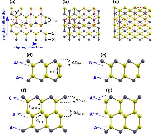
Table LABEL:table_properties presents the optimized structural parameters of the \ceSi2X2 bilayers and \ceSi4X2 trilayers, as well as the respective values obtained for pristine silicene Si2 monolayer, Si4 bilayers, and Si6 trilayers, where the distance labels are consistent with the ones defined in figure 1. The table also displays the respective standard enthalpy of formation and the dynamic stability (DS).
| Structural parameters | |||||||||||
| System | Structure | Stacking | DS | ||||||||
| Monolayer | Si2 | — | 3.870 | 2.285 | — | — | 0.482 | — | 115.67 | 751 | Yes |
| Bilayer | Si4 | AA′ | 3.854 | 2.325 | 2.470 | — | 0.676 | — | 111.89 | 609 | Yes |
| AB | 3.847 | 2.322 | 2.538 | — | 0.676 | — | 111.89 | 570 | Yes | ||
| Si2B2 | AA′ | 3.448 | 1.993 | 2.565 | — | 0.109 | — | 119.70 | 648 | No | |
| AB | 3.468 | 2.005 | 2.498 | — | 0.104 | — | 119.73 | 704 | No | ||
| Si2Al2 | AA′ | 4.231 | 2.457 | 2.572 | — | 0.271 | — | 118.79 | 446 | No | |
| AB | 4.242 | 2.457 | 2.514 | — | 0.200 | — | 119.34 | 404 | No | ||
| Si2N2 | AA′ | 2.909 | 1.767 | 2.429 | — | 0.548 | — | 110.81 | -743 | Yes | |
| AB | 2.921 | 1.771 | 2.393 | — | 0.541 | — | 111.08 | -733 | Yes | ||
| Si2P2 | AA′ | 3.544 | 2.286 | 2.380 | — | 1.019 | — | 101.65 | -87 | Yes | |
| AB | 3.557 | 2.287 | 2.351 | — | 1.007 | — | 102.06 | -84 | Yes | ||
| Trilayer | Si6 | AA′A | 3.858 | 2.332 | 2.423 | 2.355 | 0.690 | 0.756 | 111.62 | 224 | Yes |
| ABC | 3.858 | 2.333 | 2.435 | 2.355 | 0.695 | 0.764 | 111.51 | 220 | Yes | ||
| Si4B2 | AA′A′′ | 3.539 | 2.045 | 2.495 | 2.282 | 0.092 | 1.019 | 119.79 | 552 | No | |
| ABC | 3.568 | 2.061 | 2.403 | 2.272 | 0.086 | 0.900 | 119.82 | 529 | Yes | ||
| Si4Al2 | AA′A′′ | 4.128 | 2.390 | 2.439 | 2.515 | 0.175 | 0.802 | 119.46 | 339 | No | |
| ABC | 4.143 | 2.399 | 2.419 | 2.516 | 0.185 | 0.782 | 119.40 | 309 | Yes | ||
| Si4N2 | AA′A′′ | 2.911 | 1.763 | 2.384 | 2.508 | 0.533 | 1.861 | 111.27 | -156 | No | |
| ABC | 2.865 | 1.751 | 2.433 | 2.807 | 0.574 | 2.267 | 109.78 | -188 | No | ||
| Si4P2 | AA′A′′ | 3.641 | 2.321 | 2.365 | 2.283 | 0.984 | 0.890 | 103.32 | -6 | Yes | |
| ABC | 3.665 | 2.330 | 2.356 | 2.292 | 0.974 | 0.880 | 103.74 | -7 | Yes | ||
Starting with the pristine FLS, we found that the lattice constants for all of nanosystems are very close, ranging from 3.847 Å (\ceAB-Si4) to 3.870 Å (\ceSi2). On the other hand, the calculated buckling distances in the \ceSi4 and \ceSi6 layers, despite having similar values, are on the order of 43% larger than the value of 0.482 Å found in pure silicene \ceSi2 monolayer. Additionally, \ceSi2 has an intraplanar bond angle of 115.67∘, which is related to - hybridization, while the values, obtained for \ceAA′A-Si6 and \ceABC-Si6 trilayers, are 111.62∘ and 111.51∘, respectively, which are closer to the hybridization angle value of 109.47∘. As the number of layers increases, the values decrease towards the tetrahedral value, as Si atoms prefer the hybridization 38, 39. Moreover, unlike the few-layer graphene and graphite, which present weak interlayer van der Waals interactions, in the FLS the layers are covalently bonded. Accordingly, the interlayer distances are in the 2.423-2.538 Å range, the smallest one associated with the trilayers, all values close to the interatomic distance of crystalline silicon (2.352 Å). Those results are in good agreement with the ones reported in the literature 40, 13, 38, 11.
According to table LABEL:table_properties, when the silicene bilayer is 50% doped with substitutional B, Al, or P atoms, the lattice parameter changes by about 10%, decreasing in the \ceSi2B2 and \ceSi2P2 bilayers, and increasing in the \ceSi2Al2 ones, regardless of the stacking configuration. In contrast, the N atom substitution considerably affects the value, i.e., the lattice parameter decreases 25% in both \ceSi2N2 stacking configurations. Therefore, while the Al substitution stretched out the lattice parameter and the intralayer distance , in comparison with pristine silicene bilayers, the incorporation of B, N, or P atoms reduced them. The values Å and Å for, respectively, \ceSi2Al2 and \ceSi2B2 bilayers are close to the ones reported by Ding et al. 10 in the Al/B doped silicene monolayer: 2.42 Å for \ceSiAl, 2.43 Å for \ceAlSi3, 1.96 Å for \ceSiB, and 1.94 Å for \ceBSi3.
It can be noticed that in the bilayer systems functionalized with group-III atoms (B and Al, with valence electronic configuration and , respectively), the intraplanar bond angles are greater than in the pristine \ceSi4 bilayer, being very close to the value of 120∘, which is the expected value of the -type hybridization of B and Al atoms bonded to three adjacent Si atoms. Consequently, the buckling distances are greatly affected by the substitution, being reduced by about 85% in the \ceSi2B2 bilayer for both stacking configurations ( Å), by about 60% in the \ceAA′-Si2Al2 bilayer ( Å), and by about 70% in the \ceAB-Si2Al2 bilayer ( Å).
On the other hand, in the bilayer systems functionalized with group-V atoms (N and P, with valence electronic configuration and , respectively), according to table LABEL:table_properties, the intraplanar bond angles are smaller than in the pristine \ceSi4 sheet, approaching the -type hybridization angle value, with three bonds and a lone pair. Those values are a little greater than 109.47∘ for the \ceSi2N2 systems while they are smaller than that value for the \ceSi2P2 nanosheets. The P atom substitution causes major modifications in the pristine buckling distances as Å in the \ceSi2P2 bilayer, for both stacking configurations, whilst for the N atom substitution the buckling distances are Å, a value that is in the range between the ones found for pristine silicene monolayer and bilayers. The functionalized bilayers present interlayer distances slightly greater/smaller than the ones of pristine silicene bilayers, indicating that the strong Si-Si covalent bonds are maintained. Moreover, the structural parameters of \ceSi2N2 and \ceSi2P2 systems agree with the available reported data 16.
The pristine silicene \ceSi6 trilayers have lattice parameters of 3.858 Å and present additional structural parameters in comparison to the bilayer systems, namely, the intralayer and buckling distances. The Å obtained for both stacking configurations, as well as the of 0.756 Å and 0.764 Å, found in the \ceAA′A and \ceABC stacking configurations, are very close to the Si bulk values of 2.352 Å and 0.784 Å for and , respectively.
The B, Al, or P doping of \ceSi6 modify the lattice parameter by about 7%, which increases in the \ceSi4Al2 sheets and decreases in the \ceSi4B2 and \ceSi4P2 ones, irrespective of the stacking configuration. The \ceSi4P2 structures exhibit the closest lattice parameters to the one of pure silicene trilayers, in which we found lattice parameters of 3.641 and 3.665 Å for \ceAA′A′′ and \ceABC stacking configurations, respectively. Nevertheless, the presence of N affects substantially the values, decreasing them by more than 25%, as compared to that of the pristine systems, in both \ceSi4N2 stacking configurations. Those systems present the smallest lattice parameters among all trilayers studied here, consistent with the \ceSi2N2 systems among the bilayers.
The \ceSi4Al2 trilayers present lattice parameters of about 4.1 Å, with buckling distances and intraplanar bond angles of about 0.18 Å and 119.4∘, respectively. The \ceSi4B2 trilayers present Å, Å, and . As a result, those nanosheets doped with group-III atoms present low-buckled surfaces, as expected for -type hybridization in a Si host. In the trilayers functionalized with N or P atoms, the intraplanar bond angles and the intralayer and buckling distances show similar behavior to the functionalized bilayers doped with group-V atoms. Accordingly, those nanosheets present buckled surfaces.
Regarding \ceAA′A′′-Si4Al2 and \ceABC-Si4Al2 systems, the intralayer distances are, respectively, = 2.390 and 2.399 Å, which are slightly smaller than the values found for the \ceSi2Al2 bilayers. Although the Si-Si intralayer distance of around 2.52 Å is larger than the one in pure silicene trilayer (2.355 Å), silicon bulk (2.352 Å), or silicene monolayer (2.285 Å), the bond distance is still smaller than the longest Si-Si bonds (2.697 and 2.7288(15) Å) 41. These systems also present a small variation of the buckling distances, with values of 0.802 Å for \ceAA′A′′-Si4Al2 and 0.782 Å for \ceABC-Si4Al2. Additionally, the distance between layers, i.e., the Si-Si interlayer distance, is similar to that in pristine silicene trilayes (2.423 and 2.435 Å) and close to the value of 2.365 Å obtained for the hydrogenated silicene 12, showing that the Al incorporation does not disrupt the strong covalent Si-Si interactions.
As in the \ceSi4Al2 systems, the functionalized \ceSi4B2, \ceSi4N2, and \ceSi4P2 trilayers have strong Si-Si covalent bonds, presenting interlayer distance values close to the one in pristine silicene trilayers. Moreover, except for the \ceSi4N2 system, these structures present Si-Si intralayer distances close to the value in pure silicene monolayer of 2.285 Å, being 2.272 and 2.282 Å for \ceABC and \ceAA′A′′\ce-Si4B2 systems, respectively, while they are 2.292 and 2.283 Å for \ceABC and \ceAA′A′′\ce-Si4P2 systems. In contrary, the Å found for \ceABC-Si4N2 trilayer is larger than the longest known Si-Si bonds 41.
The buckling Si-Si distance of 0.756 Å and 0.764 Å for pristine silicene trilayers in the \ceAA′A and \ceABC stacking configurations, respectively, are very close to the Si bulk value of 0.784 Å. For the trilayer doped with Al, this buckling distance does not increase more than 6%, depending on the stacking configuration, when compared with pristine silicene. For the \ceSi4P2 trilayers, regardless the stacking configuration, the distance increase is of about 17%, of the same magnitude observed for the \ceSi4B2 system in the \ceABC stacking, which, however, is strongly affected, increasing by more than 34% when the stacking is \ceAA′A′′. On the other hand, the N atom substitution causes huge modifications in the pristine Si-Si buckling distances, i.e., increases about 150% for \ceAA′A′′-Si4N2 stacking arrangement and has its value practically tripled for \ceABC stacking configuration. Those major changes have important implications on the system’s dynamic stability, as will be discussed later.
3.2 Enthalpy of formation
We now discuss the possibility of synthesizing the \ceSi2X2 and \ceSi4X2 nanosheets, by analysing the values of the standard enthalpy of formation , obtained by using Eq. 2 and comparing with the values for pristine silicene structures and graphene, the most well known 2D material. The values are shown in table LABEL:table_properties.
A negative value of the enthalpy of formation indicates that the formation of a certain compound is exothermic, i.e., the amount of energy it takes to break bonds of the originating species is smaller than the amount of energy released when making the bonds. Herein, a negative indicates the systems are stable or metastable, since is a necessary but not sufficient condition for thermodynamic stability 37. Nevertheless, it is still possible to synthesize 2D materials by endothermic processes, i.e., with positive . For instance, the values of silicene and graphene monolayers are 751 meV/atom and 70 meV/atom 42, respectively. The value of silicene obtained here is in good agreement with the available results reported in the literature 43, 37.
It can be observed in table LABEL:table_properties that the calculated values for pure silicene \ceAA′-Si4 and \ceAB-Si4 bilayers are 609 and 570 meV/atom, respectively, while they are 224 and 220 meV/atom for the \ceAA′A-Si6 and \ceABC-Si6 trilayers, respectively. These results confirm the assertion that the FLS synthesis is easier than the silicene monolayer one. Particularly, it has been proposed that it is easier to experimentally produce free-standing 2D materials when the is under the threshold energy value of 200 meV/atom 44, 37, 45.
Among the structures investigated, we found that the silicene bilayer and trilayer sheets doped with substitutional N or P atoms have negative , where the exothermic reaction is likely due to the high reactivity of the silicene surface 10. The remaining systems have positive , with values ranging between the threshold (200 meV/atom) and the silicene monolayer enthalpy of formation (751 meV/atom) energies.
Regarding the \ceSi2N2 and \ceSi2P2 bilayers, whose formation are exothermic, the \ceAA′ phase is slightly more favorable than the \ceAB one. It is worth mentioning that the results for \ceSi2P2 are consistent with other results reported in the literature 46. The \ceSi2B2 bilayers are the least energetically favorable systems since they present the largest values of 648 and 704 meV/atom for \ceAA′ and \ceAB stacking, respectively, which is higher than the value found for pristine silicene bilayers. Oppositely, the \ceSi2Al2 sheets are energetically more favorable than pure silicene bilayers since we found smaller values of 446 and 404 meV/atom for the \ceAA′ and \ceAB stacking configurations.
The doped silicene trilayers present a similar behavior as the bilayers: while the \ceSi4B2 systems present the highest positive among all \ceSi4X2 structures, the \ceSi4N2 exhibit the lowest negative ones. Besides, the silicene trilayers doped with B or Al atoms are energetically less favorable than the pristine silicene trilayers, while the P doped ones present negative values.
3.3 Dynamic stability and elasticity
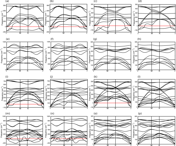
To establish the structures’ dynamic stability, we used the phonon theory to obtain the respective vibrational spectra. A certain structure is dynamically stable when it has only positive frequencies in the respective phonon dispersion curves. Table LABEL:table_properties presents the stability of all structures investigated here based on that criteria (DS). According to the table, silicene bilayers and trilayers functionalized with P atoms are dynamically stable. On the other hand, silicene structures functionalized with B, Al, or N are dynamically stable only in some stacking configurations.
The structures’ phonon dispersion curves are presented in Fig. 2. Both stacking configurations of \ceSi2B2 and \ceSi2Al2 bilayers (Fig. 2(a), (b), (c), and (d)) and of \ceSi4N2 trilayers (Fig. 2(m) and (n)), as well as the \ceAA′A′′-Si4B2 system (Fig. 2(i)) and \ceAA′A′′-Si4Al2 trilayer (Fig. 2(k)), present large negative frequencies and, hence, they are dynamically unstable. Moreover, the small negative frequency around the valley in the \ceABC-Si4B2 system, shown in Fig. 2(j), could indicate that this sheet has lower stability than the other dynamically stable trilayers studied here. This behavior has been found in some theoretical investigations of 2D materials, and has been generally associated with the difficulty in converging the out-of-plane ZA transverse acoustic mode 47, 17.
We computed the elastic constants of the systems with Eq. 1, which must satisfy and for elastic stability (Born stability criteria) 48. Moreover, for the dynamically stable (DS) bilayers and trilayers presented in table LABEL:table_properties, we also evaluated the \ceC44 elastic constant through expression, the Young modulus , and the Poisson ratio . The results are displayed in table LABEL:table_elastic, which confirm what was observed in the phonon dispersion spectra shown in figure 2, regarding the stability of the compounds, once all the dynamically stable systems satisfy the Born criteria. For the pristine silicene monolayer, the calculated values for all the elastic constants are in concordance with data from the literature 10. Moreover, the \ceC11 elastic constant of the pure \ceAB-Si4 bilayer of 121 N/m and \ceABC-Si6 trilayer of 167 N/m are also in agreement with previously reported results 38.
| System | Structure | Stacking | C11 | C12 | C44 | ||
|---|---|---|---|---|---|---|---|
| Monolayer | Si2 | — | 69 | 19 | 25 | 64 | 0.28 |
| Bilayer | Si4 | AA′ | 124 | 36 | 44 | 113 | 0.29 |
| AB | 121 | 33 | 43 | 111 | 0.28 | ||
| Si2N2 | AA′ | 296 | 83 | 106 | 273 | 0.28 | |
| AB | 278 | 83 | 97 | 252 | 0.30 | ||
| Si2P2 | AA′ | 133 | 24 | 55 | 129 | 0.18 | |
| AB | 129 | 23 | 53 | 125 | 0.18 | ||
| Trilayer | Si6 | AA′A | 157 | 33 | 62 | 150 | 0.21 |
| ABC | 167 | 43 | 62 | 156 | 0.25 | ||
| Si4B2 | ABC | 198 | 35 | 82 | 192 | 0.17 | |
| Si4Al2 | ABC | 123 | 84 | 20 | 66 | 0.68 | |
| Si4P2 | AA′A′′ | 182 | 38 | 72 | 174 | 0.21 | |
| ABC | 176 | 36 | 70 | 168 | 0.21 |
Additionally, we observe that pristine FLS structures are more stable as they grow in thickness, i.e., the elastic constants and the increase with the number of layers 38. For the functionalized FLS, the values range from 66 to 273 N/m, which are directly related to the systems’ lattice parameter and intralayer distances . The \ceSi2N2 bilayers have the smallest and the largest , while the \ceABC-Si4Al2 trilayer has the largest and the lowest . The remaining systems follow the same trend, which has also been observed in other 2D systems 39. Furthermore, except for the \ceABC-Si4Al2, all the systems investigated have Poisson ratio between 0.17 and 0.30, in the 0-0.5 range which has been observed in 2D materials 39 and isotropic systems 49. Although the value of 0.68 obtained for the \ceABC-Si4Al2 trilayer is larger than 0.5, it is similar to values found in stretched silicene monolayer of 0.62 50 and 0.75 51. Indeed, the Al atom substitution in pristine silicene trilayer increases the lattice parameter and, hence, the Si-Si bond distances.
Our results show that the stability of the binary bilayers depends on the X atoms, as we find that the combination between group-V and group-IV elements, as in \ceSi2N2 and \ceSi2P2 structures, produces dynamically stable systems as they exhibit only positive frequencies and satisfy the Born stability criteria. On the other hand, there is no dynamic stability for the compounds that involve combinations of group-III and group-IV elements, i.e., \ceSi2B2 and \ceSi2Al2 bilayers.
In the trilayers, the stable systems are \ceABC-Si4B2, \ceABC-Si4Al2, \ceAA′A′′-Si4P2, and \ceABC-Si4P2, in which the higher structural stability is related to the system with shorter interlayer distances , which leads to the strong interactions between layers 12. The instability in the \ceABC-Si4N2 compound is likely associated with the large Si-Si intralayer bond distance of 2.807 Å and the huge buckling distance of 2.267 Å in the non-doped intermediate silicene layer. The is larger than the longest Si-Si bonds (2.697 and 2.7288(15) Å) 41 and the huge is related to the multilayer silicene instability 11. As in the \ceABC-Si4N2 system, the instability of the \ceAA′A′′-Si4N2 is also due to the large Si-Si intralayer bond distance Å and the huge buckling distance Å. Regarding the \ceAA′A′′-Si4B2 and \ceAA′A′′-Si4Al2 structures, they present similar behavior since there is a huge negative frequency around the valley, suggesting that a possible synthesis of \ceSi4B2 and \ceSi4Al2 trilayers should be in the \ceABC stacking configuration.
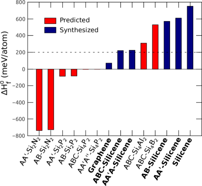
Figure 3 shows the standard enthalpy of formation for all the dynamically stable structures found here. The empirical threshold energy (200 meV/atom) to experimentally synthesize free-standing 2D materials 44, 37, 45 is also shown. Although FLS has enthalpies of formation greater than 200 meV, they have been free-standing synthesized 15. The graphene enthalpy of formation is also included for comparison, which was computed, with respect to graphite, computed using the van der Waals density functional (optB88-vdW) to describe the exchange-correlation energy 42. The comparison show the feasibility of experimentally synthesizing, through different techniques, the dynamically stable systems investigated here.
3.4 Electronic properties
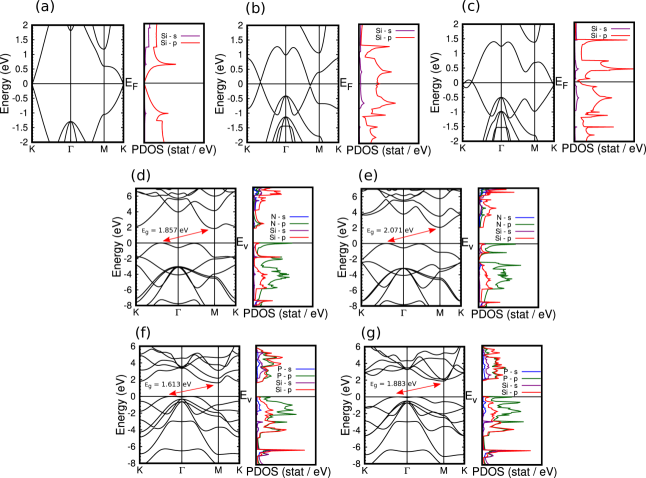
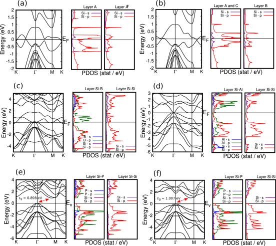
Figures 4 and 5 display the electronic band structures and the projected density of states (PDOS) of the dynamically stable \ceSi2X2 and \ceSi4X2 systems (X= B, N, Al, P), as well as the ones of the pristine silicene monolayer \ceSi2, bilayers \ceSi4, and trilayers \ceSi6. Table LABEL:table_electronic presents the systems’ classification and list the values of the indirect electronic band gaps , the high-symmetry point or direction of the valence band maximum (VBM) and conduction band minimum (CBM), and their atomic character.
Previous studies have shown that pure silicene monolayer has zero band gap with a Dirac cone at the K-point in the Brillouin zone 4 and FLS can present metallic or semiconducting behavior depending on the stacking configuration 13, 14, 11. All of our results for pristine silicene structures, displayed in Fig. 4(a) for \ceSi2, Fig. 4(b) and (c) for \ceSi4, and Fig. 5(a) and (b) for \ceSi6, agree well with the ones reported in the literature, where the investigated FLS are metallic structures. For the functionalized FLS, we found that the \ceAA′-Si2N2, \ceAB-Si2N2, \ceAA′-Si2P2, and \ceAB-Si2P2 doped bilayers, Fig. 4 (d)-(g), and the \ceAA′A′′-Si4P2 and \ceABC-Si4P2 doped trilayers, Fig. 5(e) and (f), are indirect band gap semiconductors, while the \ceABC-Si4B2 and \ceABC-Si4Al2 trilayers, Fig. 5(c) and (d), are metallic. It should be noticed that these band gap values should be considered as lower limits, as the DFT/vdW is known to underestimate them.
| System | Structure | Stacking | Classification | VBM (character) | CBM (character) | |
|---|---|---|---|---|---|---|
| Monolayer | Si2 | — | semimetal | 0 | — | — |
| Bilayer | Si4 | AA′ | metal | — | — | — |
| AB | metal | — | ||||
| Si2N2 | AA′ | semiconductor | 1.857 | K- (Si-, N-) | M (Si-, N-) | |
| AB | semiconductor | 2.071 | K- (Si-, N-) | M (Si-) | ||
| Si2P2 | AA′ | semiconductor | 1.613 | K- (Si-, P-) | M (Si-, P-) | |
| AB | semiconductor | 1.883 | K- (Si-, P-) | M (Si-, P-) | ||
| Trilayer | Si6 | AA′A | metal | — | — | — |
| ABC | metal | — | ||||
| Si4B2 | ABC | metal | — | — | — | |
| Si4Al2 | ABC | metal | — | — | — | |
| Si4P2 | AA′A′′ | semiconductor | 0.898 | (Si-) | -M (Si-, P-) | |
| ABC | semiconductor | 1.007 | (Si-) | -M (Si-, P-) |
The differences in the electronic properties result from the distinct \ceX doping elements that composed the systems, i.e., the prevailing factor that determined the properties of the compounds is the number of valence electrons of the X atoms. The group-V atoms (N, P) substitution transforms the pristine silicene bilayers and trilayers from metallic to semiconductor. In contrast, the B or Al substitution keeps the metallic behavior of pristine silicene trilayers. Additionally, the Dirac cone in the metallic pristine silicene trilayers, which is below the Fermi energy at the K-point for \ceAA′A stacking configuration, Fig. 5(a), and in the K-M direction for \ceABC one, Fig. 5(b) 11, is not preserved in the \ceSi4X2 systems. The electronic band gaps () for \ceAA′-Si2N2, \ceAB-Si2N2, \ceAA′-Si2P2, \ceAB-Si2P2, \ceAA′A′′-Si4P2, and \ceABC-Si4P2, are 1.857, 2.071, 1.613, 1.883, 0.898, and 1.007 eV, respectively. The values of \ceSi2N2 and \ceSi2P2 functionalized bilayers are in good agreement with reported theoretical results that used the PBE functional approximation for the exchange-correlation energy, values that increased by up to 1 eV (\ceSi2N2) and 0.7 eV (\ceSi2P2) when the Heyd-Scuseria-Ernzerhof screen-exchange hybrid functional (HSE06) was used 16, suggesting that the electronic band gaps presented in table LABEL:table_electronic are likely underestimated by at least 0.7 eV.
For the \ceSi2N2 and \ceSi2P2 semiconducting bilayers, Fig. 4 (d)-(g) show that the bottom of the conduction band, at M-point, and the top of the valence band, at the high-symmetry K- direction, have contributions mainly from the hybridization of the Si and X -states (X = N, P), with prevailing X -states character. Moreover, the top region of the valence band is highly degenerated with a Mexican-hat dispersion (quartic function), in accordance with other investigations 16.
The \ceAA′A′′-Si4P2 and \ceABC-Si4P2 semiconducting trilayers have similar band structures and PDOS, as shown in Fig. 5 (e) and (f), with the VBM at the -point and the CBM at the -M direction. The PDOS shows that the Si -orbitals derived from the intermediate (non-doped) Si-Si layer and from the Si-P layer dominate at the VBM, while at the CBM there is also a contribution of the P -states from the Si-P layer. In the \ceABC-Si4B2 and \ceABC-Si4Al2 metallic systems, Fig. 5 (c) and (d), the Fermi level crosses three bands, in the -point region, that have contributions from the hybridization of the Si and X -orbitals of the Si-X layer (X = B, Al), and from the Si -state of the Si-Si layer. Moreover, the Fermi level crossing around the K-point in the \ceABC-Si4B2 is mainly derived from the B -states of the Si-B layer and from Si -states of the Si-Si layer.
These results provide chemical routes to tune and control the FLS electronic structure by increasing the number of layers and, at the same time, doping them to be used in specific applications.
4 Discussion and Concluding Remarks
In summary, we performed a theoretical investigation on the structural, energetic, dynamic, elastic, and electronic properties of silicene bilayers and trilayers functionalized with group-III and group-V atoms in several stacking configurations. We identified a number of functionalized FLS that are dynamically stable and experimentally accessible, based on the results of the enthalpies of formation, phonon dispersion spectra, and Born stability criteria. Additionally, among them we found that two structures present metallic behavior while the others present semiconducting properties, accordingly to the respective electronic structures, which are directly associated with the atomic species used in the functionalization.
The \ceABC-Si4B2 and \ceABC-Si4Al2 metallic systems present low-buckled surfaces, being the least favorable of the structures studied since they have the greatest positive enthalpy of formation. However, the enthalpies of formation of these systems are still lower than that of pristine silicene monolayer, which has already been synthesized. In particular, the \ceAA′A′′-Si4P2 and \ceABC-Si4P2 semiconductor trilayers present an enthalpy of formation nearly zero, i.e., which is lower than the empirical threshold energy of 200 meV/atom for the synthesis of free-standing 2D materials and, therefore, considering the recent synthesis of several 2D materials, the structures studied here are likely to be produced in a near future.
Further investigations could explore the applicability of the structures propose here. Previous studies have shown that functionalized nanostructures could serve as building blocks for the self-assembly of complex 3D systems 52, 2, 42. Particularly, 2D building blocks could be vertically combined to make 2D/3D systems with tailored properties 2, 42. Recently, van der Waals heterostructures based on silicon \ceSiX (X = N, P, As, Sb, Bi) have been investigated in several stacking configurations, in which the \ceSiN was proposed for water oxidation applications and the \ceSiP for photocatalytic water splitting 53. Therefore, considering the silicon-based structures investigated here, it is interesting to explore if those systems could be used as building blocks and how their properties would modify with different morphologies. The \ceSi2N2 and \ceSi2P2 bilayers have been considered for UV-light applications due to their wide band gap 16 and as thermoelectric materials at room temperature 54. Within such context, the \ceAA′A′′-Si4P2 and \ceABC-Si4P2 nanosheets could be explored as thermoelectric materials. Although we found a narrower band gap for these systems in comparison with \ceSi2P2 bilayers, it is important once more emphasizing that the band gap is here underestimated due to the DFT/vdW approximation and, hence, we suggest the \ceAA′A′′-Si4P2 and \ceABC-Si4P2 semiconducting trilayers could be appropriated for UV-light application as well.
Moreover, silicene monolayer and FLS nanosheets are promising candidates for energy storage system applications, such as lithium-ion batteries 55, 15. Peculiarly, the silicene monolayer doped with different elements has shown good performance for alkali metal ion batteries (AMIBs). For instance, B/Al doped silicene has low diffusion barriers and higher capacity for sodium-ion batteries (SIBs) and potassium-ion batteries (KIBs) in comparison to pristine silicene 56. Therefore, since good electrical conductivity is one of the requirements for advantageous electrodes 57, the \ceABC-Si4B2 and \ceABC-Si4Al2 metallic structures are promising candidates for AMIBs applications.
This investigation was partially supported by Brazilian federal government agencies CAPES and CNPq. The authors acknowledge the National Laboratory for Scientific Computing (LNCC/MCTI, Brazil) for providing HPC resources of the Santos Dumont supercomputer (http://sdumont.lncc.br) and Centro Nacional de Processamento de Alto Desempenho em São Paulo (CENAPAD-SP, Brazil). LVCA and JFJ acknowledge support from Brazilian agency CNPq, under projects numbers 305753/2017-7 and 305187/2018-0.
References
- Novoselov et al. 2004 Novoselov, K. S.; Geim, A. K.; Morozov, S. V.; Jiang, D.; Zhang, Y.; Dubonos, S. V.; Grigorieva, I. V.; Firsov, A. A. Electric field effect in atomically thin carbon films. Science 2004, 306, 666–669
- Novoselov et al. 2016 Novoselov, K. S.; Mishchenko, A.; Carvalho, A.; Castro Neto, A. H. 2D materials and van der Waals heterostructures. Science 2016, 353, aac9439
- Li et al. 2018 Li, G.; Zhang, Y.-Y.; Guo, H.; Huang, L.; Lu, H.; Lin, X.; Wang, Y.-L.; Du, S.; Gao, H.-J. Epitaxial growth and physical properties of 2D materials beyond graphene: from monatomic materials to binary compounds. Chemical Society Reviews 2018, 47, 6073–6100
- Cahangirov et al. 2009 Cahangirov, S.; Topsakal, M.; Aktürk, E.; Şahin, H.; Ciraci, S. Two- and one-dimensional honeycomb structures of silicon and germanium. Physical Review Letters 2009, 102, 236804
- Garcia et al. 2011 Garcia, J. C.; de Lima, D. B.; Assali, L. V. C.; Justo, J. F. Group IV graphene- and graphane-like nanosheets. The Journal of Physical Chemistry C 2011, 115, 13242–13246
- Schoop et al. 2018 Schoop, L. M.; Pielnhofer, F.; Lotsch, B. V. Chemical principles of topological semimetals. Chemistry of Materials 2018, 30, 3155–3176
- Molle et al. 2018 Molle, A.; Grazianetti, C.; Tao, L.; Taneja, D.; Alam, M. H.; Akinwande, D. Silicene, silicene derivatives, and their device applications. Chemical Society Reviews 2018, 47, 6370–6387
- Zhuang et al. 2015 Zhuang, J.; Xu, X.; Feng, H.; Li, Z.; Wang, X.; Du, Y. Honeycomb silicon: a review of silicene. Science Bulletin 2015, 60, 1551–1562
- Sivek et al. 2013 Sivek, J.; Sahin, H.; Partoens, B.; Peeters, F. M. Adsorption and absorption of boron, nitrogen, aluminum, and phosphorus on silicene: Stability and electronic and phonon properties. Physical Review B 2013, 87, 085444
- Ding and Wang 2013 Ding, Y.; Wang, Y. Density functional theory study of the silicene-like \ceSiX and \ceXSi3 (X= B, C, N, Al, P) honeycomb lattices: the various buckled structures and versatile electronic properties. The Journal of Physical Chemistry C 2013, 117, 18266–18278
- Qian and Li 2020 Qian, C.; Li, Z. Multilayer silicene: structure, electronics, and mechanical property. Computational Materials Science 2020, 172, 109354
- Liu et al. 2013 Liu, Y.; Shu, H.; Liang, P.; Cao, D.; Chen, X.; Lu, W. Structural, electronic, and optical properties of hydrogenated few-layer silicene: size and stacking effects. Journal of Applied Physics 2013, 114, 094308
- Padilha and Pontes 2015 Padilha, J. E.; Pontes, R. B. Free-standing bilayer silicene: the effect of stacking order on the structural, electronic, and transport properties. The Journal of Physical Chemistry C 2015, 119, 3818–3825
- Fu et al. 2014 Fu, H.; Zhang, J.; Ding, Z.; Li, H.; Meng, S. Stacking-dependent electronic structure of bilayer silicene. Applied Physics Letters 2014, 104, 131904
- Liu et al. 2018 Liu, J.; Yang, Y.; Lyu, P.; Nachtigall, P.; Xu, Y. Few-layer silicene nanosheets with superior lithium-storage properties. Advanced Materials 2018, 30, 1800838
- Özdamar et al. 2018 Özdamar, B.; Özbal, G.; Çınar, M. N.; Sevim, K.; Kurt, G.; Kaya, B.; Sevinçli, H. Structural, vibrational, and electronic properties of single-layer hexagonal crystals of group IV and V elements. Physical Review B 2018, 98, 045431
- Touski and Ghobadi 2021 Touski, S. B.; Ghobadi, N. Structural, electrical, and Rashba properties of monolayer Janus \ceSi2XY (X, Y= P, As, Sb, and Bi). Physical Review B 2021, 103, 165404
- Yang et al. 2016 Yang, J.-H.; Zhang, Y.; Yin, W.-J.; Gong, X.; Yakobson, B. I.; Wei, S.-H. Two-dimensional SiS layers with promising electronic and optoelectronic properties: theoretical prediction. Nano Letters 2016, 16, 1110–1117
- An et al. 2020 An, Y.; Tian, Y.; Wei, C.; Zhang, Y.; Xiong, S.; Feng, J.; Qian, Y. Recent advances and perspectives of 2D silicon: synthesis and application for energy storage and conversion. Energy Storage Materials 2020, 32, 115–150
- Tantardini et al. 2021 Tantardini, C.; Kvashnin, A. G.; Gatti, C.; Yakobson, B. I.; Gonze, X. Computational modeling of 2D materials under high pressure and their chemical bonding: silicene as possible field-effect transistor. ACS Nano 2021, 15, 6861–6871
- Giannozzi et al. 2009 Giannozzi, P.; Baroni, S.; Bonini, N.; Calandra, M.; Car, R.; Cavazzoni, C.; Ceresoli, D.; Chiarotti, G. L.; Cococcioni, M.; Dabo, I. et al. QUANTUM ESPRESSO: a modular and open-source software project for quantum simulations of materials. Journal of physics: Condensed matter 2009, 21, 395502
- Giannozzi et al. 2017 Giannozzi, P.; Andreussi, O.; Brumme, T.; Bunau, O.; Nardelli, M. B.; Calandra, M.; Car, R.; Cavazzoni, C.; Ceresoli, D.; Cococcioni, M. et al. Advanced capabilities for materials modelling with Quantum ESPRESSO. Journal of Physics: Condensed Matter 2017, 29, 465901
- Hohenberg and Kohn 1964 Hohenberg, P.; Kohn, W. Inhomogeneous electron gas. Physical Review 1964, 136, B864
- Kohn and Sham 1965 Kohn, W.; Sham, L. J. Self-consistent equations including exchange and correlation effects. Physical Review 1965, 140, A1133
- Kresse and Joubert 1999 Kresse, G.; Joubert, D. From ultrasoft pseudopotentials to the projector augmented-wave method. Physical Review B 1999, 59, 1758–1775
- Perdew et al. 1996 Perdew, J. P.; Burke, K.; Ernzerhof, M. Generalized gradient approximation made simple. Physical Review Letters 1996, 77, 3865
- Dion et al. 2004 Dion, M.; Rydberg, H.; Schröder, E.; Langreth, D. C.; Lundqvist, B. I. Van der Waals density functional for general geometries. Physical Review Letters 2004, 92, 246401
- Klimeš et al. 2009 Klimeš, J.; Bowler, D. R.; Michaelides, A. Chemical accuracy for the van der Waals density functional. Journal of Physics: Condensed Matter 2009, 22, 022201
- Zhang et al. 2011 Zhang, G.-X.; Tkatchenko, A.; Paier, J.; Appel, H.; Scheffler, M. Van der Waals interactions in ionic and semiconductor solids. Physical Review Letters 2011, 107, 245501
- Park et al. 2015 Park, J.; Yu, B. D.; Hong, S. Van der Waals density functional theory study for bulk solids with BCC, FCC, and diamond structures. Current Applied Physics 2015, 15, 885–891
- Marcondes et al. 2018 Marcondes, M. L.; Wentzcovitch, R. M.; Assali, L. V. C. Importance of van der Waals interaction on structural, vibrational, and thermodynamic properties of NaCl. Solid State Communications 2018, 273, 11–16
- Monkhorst and Pack 1976 Monkhorst, H. J.; Pack, J. D. Special points for Brillouin-zone integrations. Physical Review B 1976, 13, 5188–5192
- Baroni et al. 2001 Baroni, S.; De Gironcoli, S.; Dal Corso, A.; Giannozzi, P. Phonons and related crystal properties from density-functional perturbation theory. Reviews of Modern Physics 2001, 73, 515–562
- Cadelano et al. 2010 Cadelano, E.; Palla, P. L.; Giordano, S.; Colombo, L. Elastic properties of hydrogenated graphene. Physical Review B 2010, 82, 235414
- Assali et al. 2006 Assali, L. V. C.; Machado, W. V. M.; Justo, J. F. Manganese impurities in boron nitride. Applied Physics Letters 2006, 89, 072102
- Assali et al. 2011 Assali, L. V. C.; Machado, W. V. M.; Justo, J. F. 3d transition metal impurities in diamond: electronic properties and chemical trends. Physical Review B 2011, 84, 155205
- Haastrup et al. 2018 Haastrup, S.; Strange, M.; Pandey, M.; Deilmann, T.; Schmidt, P. S.; Hinsche, N. F.; Gjerding, M. N.; Torelli, D.; Larsen, P. M.; Riis-Jensen, A. C. et al. The computational 2D materials database: high-throughput modeling and discovery of atomically thin crystals. 2D Materials 2018, 5, 042002
- Li et al. 2019 Li, Y.; Tang, G.; Fu, B. Hydrogenation: an effective strategy to improve the thermoelectric properties of multilayer silicene. Physical Review B 2019, 99, 235428
- Hess 2021 Hess, P. Bonding, structure, and mechanical stability of 2D materials: the predictive power of the periodic table. Nanoscale Horizons 2021, 6, 856–892
- Kamal et al. 2013 Kamal, C.; Chakrabarti, A.; Banerjee, A.; Deb, S. Silicene beyond mono-layers different stacking configurations and their properties. Journal of Physics: Condensed Matter 2013, 25, 085508
- Kyushin et al. 2020 Kyushin, S.; Kurosaki, Y.; Otsuka, K.; Imai, H.; Ishida, S.; Kyomen, T.; Hanaya, M.; Matsumoto, H. Silicon–silicon single bond. Nature Communications 2020, 11, 1–7
- Ipaves et al. 2019 Ipaves, B.; Justo, J. F.; Assali, L. V. C. Carbon-related bilayers: nanoscale building blocks for self-assembly nanomanufacturing. The Journal of Physical Chemistry C 2019, 123, 23195–23204
- Revard et al. 2016 Revard, B. C.; Tipton, W. W.; Yesypenko, A.; Hennig, R. G. Grand-canonical evolutionary algorithm for the prediction of two-dimensional materials. Physical Review B 2016, 93, 054117
- Ashton et al. 2016 Ashton, M.; Sinnott, S. B.; Hennig, R. G. Computational discovery and characterization of polymorphic two-dimensional IV–V materials. Applied Physics Letters 2016, 109, 192103
- Gjerding et al. 2021 Gjerding, M.; Taghizadeh, A.; Rasmussen, A.; Ali, S.; Bertoldo, F.; Deilmann, T.; Holguin, U.; Knøsgaard, N.; Kruse, M.; Manti, S. et al. Recent progress of the computational 2D materials database (C2DB). 2D Materials 2021, 8, 044002
- Huang et al. 2015 Huang, B.; Zhuang, H. L.; Yoon, M.; Sumpter, B. G.; Wei, S.-H. Highly stable two-dimensional silicon phosphides: different stoichiometries and exotic electronic properties. Physical Review B 2015, 91, 121401
- Mohebpour et al. 2020 Mohebpour, M. A.; Mozvashi, S. M.; Vishkayi, S. I.; Tagani, M. B. Prediction of hydrogenated group IV–V hexagonal binary monolayers. Scientific Reports 2020, 10, 1–14
- Mouhat and Coudert 2014 Mouhat, F.; Coudert, F.-X. Necessary and sufficient elastic stability conditions in various crystal systems. Physical Review B 2014, 90, 224104
- Gercek 2007 Gercek, H. Poisson’s ratio values for rocks. International Journal of Rock Mechanics and Mining Sciences 2007, 44, 1–13
- Wang et al. 2014 Wang, B.; Wu, J.; Gu, X.; Yin, H.; Wei, Y.; Yang, R.; Dresselhaus, M. Stable planar single-layer hexagonal silicene under tensile strain and its anomalous Poisson’s ratio. Applied Physics Letters 2014, 104, 081902
- Das and Sarkar 2018 Das, D.; Sarkar, J. Comparison of mechanical properties of silicene estimated using different testing procedures: a molecular dynamics study. Journal of Applied Physics 2018, 123, 044304
- Garcia et al. 2009 Garcia, J. C.; Justo, J. F.; Machado, W. V. M.; Assali, L. V. C. Functionalized adamantane: building blocks for nanostructure self-assembly. Physical Review B 2009, 80, 125421
- Somaiya et al. 2021 Somaiya, R.; Singh, D.; Sonvane, Y. K.; Gupta, S. K.; Ahuja, R. Potential SiX (X= N, P, As, Sb, Bi) homo-bilayers for visible-light photocatalysts application. Catalysis Science & Technology 2021, 11, 4996–5013
- Somaiya et al. 2020 Somaiya, R. N.; Sonvane, Y. A.; Gupta, S. K. Exploration of the strain and thermoelectric properties of hexagonal SiX (X= N, P, As, Sb, and Bi) monolayers. Physical Chemistry Chemical Physics 2020, 22, 3990–3998
- Zhuang et al. 2017 Zhuang, J.; Xu, X.; Peleckis, G.; Hao, W.; Dou, S. X.; Du, Y. Silicene: a promising anode for lithium-ion batteries. Advanced Materials 2017, 29, 1606716
- Zhu et al. 2018 Zhu, J.; Gandi, A. N.; Schwingenschlögl, U. Potential of B/Al-doped silicene electrodes in Na/K-ion batteries. Advanced Theory and Simulations 2018, 1, 1800017
- Zhang et al. 2021 Zhang, C.; Wang, F.; Han, J.; Bai, S.; Tan, J.; Liu, J.; Li, F. Challenges and recent progress on silicon-based anode materials for next-generation lithium-ion batteries. Small Structures 2021, 6, 2170015