Ultrahigh inductance superconducting materials from spinodal decomposition
Abstract
Disordered superconducting nitrides with kinetic inductance have long been considered a leading material candidate for high-inductance quantum-circuit applications. Despite continuing efforts in reducing material dimensions to increase the kinetic inductance and the corresponding circuit impedance, it becomes a fundamental challenge to improve further without compromising material qualities. To this end, we propose a method to drastically increase the kinetic inductance of superconducting materials via spinodal decomposition while keeping a low microwave loss. We use epitaxial Ti0.48Al0.52N as a model system, and for the first time demonstrate the utilization of spinodal decomposition to trigger the insulator-to-superconductor transition with a drastically enhanced material disorder. The measured kinetic inductance has increased by 2-3 orders of magnitude compared with all the best reported disordered superconducting nitrides. Our work paves the way for substantially enhancing and deterministically controlling the inductance for advanced superconducting quantum circuits.
I Introduction
Superconducting materials with high kinetic inductance offer new opportunities in the design of high-sensitivity photon detectors, wideband quantum amplifiers, and high-coherence quantum processors [1, 2, 3, 4]. In particular, for the noise-resilient superconducting-qubits, a non-dissipative circuit element as characterized by a considerably high inductance (i.e., several hundred nanohenry to a few microhenry) is indispensable for charge- and flux-noise protection [5, 6, 7, 8, 9, 10]. The magnitude of such inductance, as it is often the case, utterly exceeds the achievable geometric inductance in the nanofabricated superconducting circuits, making the utilization of intrinsic material properties such as kinetic inductance essential for its practical realizations. Extensive research have thus been performed on superconducting materials with a large kinetic inductance, such as Josephson-junction arrays (JJAs) [11, 12, 10, 7] and granular aluminum [13, 14, 15, 16], for the high-inductance implementations.
In addition to aluminum-based materials, disordered superconducting nitrides (e.g., TiN, NbN, NbTiN) are also drawing increasing interests. Owing to the low energy dissipation, resilience to magnetic fields, and process compatibility, these emerging materials are advantageous for high-coherence applications and large-scale circuit integration [17, 18, 19, 20, 21]. Nevertheless, due to the relatively small kinetic inductance (i.e., on the order of picohenry-per-square), a nanowire with large aspect ratio is inevitably required for the implementation of high-inductance elements [22, 23, 24, 25, 26]. Any imperfection of the nanowire could be a source of energy dissipation and deteriorate the circuit coherence. As a result, tremendous research efforts have been made in the geometric control and optimization of these materials for the practical applications [17, 25, 27, 26].
A strategy to alleviate the stringent geometric constraints is to further increase the intrinsic kinetic inductance. Primarily, this was attained by either reducing material thickness or increasing the disorder. For instance, thin films of TiN or NbN have been shown to yield a sheet inductance of several hundred picohenry-per-square as the film is thinner than 10 nm [20, 23, 28, 27]. The chemical and structural disorder in NbTiN can also be increased if the deposition techniques and parameters are properly refined [29, 24]. However, despite the continuing optimization in the material synthesis, it remains a fundamental challenge to control the homogeneity of ultrathin films where a slight variation in thickness will inevitably result in substantial changes in the material properties. It is also known that ultrathin and disordered superconducting films are accompanied by large spacial fluctuations on the superconducting order parameter [28, 30, 31, 32], which could trap quasiparticles in the superconductors and act as detrimental two-level systems [33]. Moreover, the high defect density at the surfaces and edges of ultrathin nanowires typically plays a more significant role in deteriorating the microwave performance due to the larger filing factors of electric-field energy at these two regions [34, 17, 25, 23, 35]. As such, aside from the augmentation of kinetic inductance by solely geometric reduction, an approach to intrinsically enhance the material disorder without compromising the material quality is desired.
In this work, we demonstrate a method to substantially increase the disorder and the kinetic inductance of epitaxial-quality superconducting materials with low microwave losses. The idea is to utilize the spinodal decomposition in a compound where the spontaneous phase segregation results in a much stronger chemical and structural disorder. An extensively studied material Ti0.48Al0.52N (TAN) was used as a model system to verify the feasibility of this approach. Although this material has long been considered for hard coating [36, 37], the combination of TiN (which is a superconductor) and AlN (which is a wide band-gap insulator) makes it ideal for the introduction of low-loss non-superconducting phases in the superconducting phases. We show that, the as-grown TAN epitaxial films on sapphire substrates were insulating, while after the phase segregation, an insulator-to-superconductor transition was observed. Structural characterization on the phase-segregated materials revealed good crystallinity and a random distribution of Ti-rich and Al-rich regions, consistent with our simulations and the previous studies on similar spinodal systems [38, 36]. Subsequent transport and cryogenic measurements on microwave resonators have shown a sharply enhanced sheet inductance of pH/ for the TAN films as thick as 100 nm, and a reasonably good resonator quality factor of . As the film thickness was reduced to intermediate value of 20 nm, the sheet inductance was measured to be as large as nH/, nearly 2-3 orders of magnitude higher than all the reported nitride superconductors and comparable to the highest sheet inductance ever achieved in the granular-aluminum system [20, 23, 25, 18, 17, 24, 16, 14, 15, 39, 40]. Our results demonstrate that the spinodal TAN films are promising candidates for the implementation of high-inductance and low-dissipation circuit elements. With a systematic engineering over the chemical compositions and micro-structures, spinodal superconducting systems may offer an unprecedented opportunity in the high-impedance superconducting quantum circuits.
II Spinodal decomposition and structural characterization
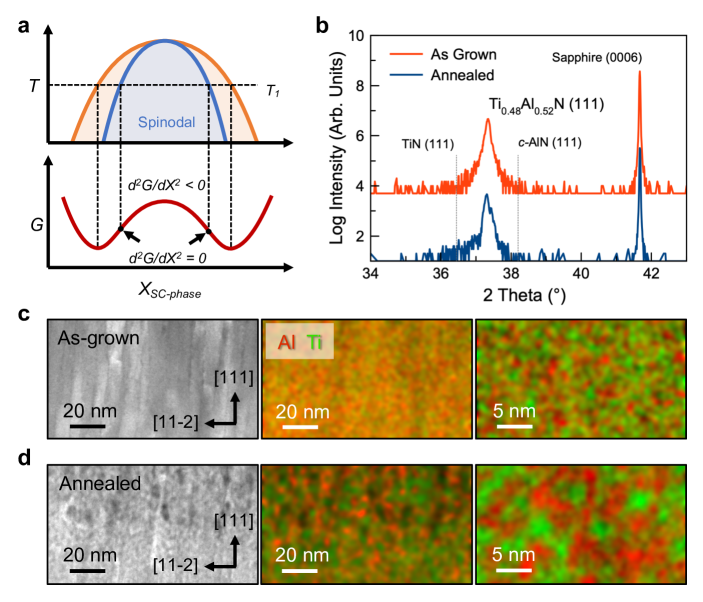
Spinodal decomposition is a spontaneous phase segregation process in mixtures where an infinitesimal perturbation can drive the segregation of phases without nucleation. Given a homogeneous solid mixture composed of two thermodynamically stable phases, the spinodal decomposition takes place in a range of compositions where the second derivative of the total Gibbs free energy is negative (Fig. 1a). Within this regime, any infinitesimal change in the material composition reduces the total energy, giving rise to a random distribution of segregated phases. Such phase segregation, in turn, creates a stronger chemical and structural disorder in the system and drastically changes the material properties. For example, given that one of the phases is a superconductor (e.g., TiN) and the other is an insulator (e.g., AlN), we have simulated the redistribution of atoms and acquired a microscopic structure with the Ti-rich regions largely confined by Al-rich regions (Supplementary Fig. 1). It can be further hypothesized that, as the phase segregation evolves, an insulator-to-superconductor transition could be observed in the Ti-rich regions, and the spinodal system manifests as a highly-disordered superconducting material. In this spirit, we carried out a set of detailed studies on a model epitaxial TAN films to verify this hypothesis.
100nm-thick epitaxial TAN thin films with a nominal stoichiometry Ti0.5Al0.5N were grown on the -cut sapphire substrates using a magnetron co-sputtering system (see Methods). Part of the deposited wafers from the same batch were annealed for phase segregation as comparative studies (i.e., 1000 ∘C for 30 mins, see Methods). From the X-ray line scans (Fig. 1b, Supplementary Fig. 2a), the as-grown TAN films are revealed to be epitaxial and single-phase as indicated by the clean and sharp diffraction peaks at the 111-diffraction conditions. Based on the diffraction peak positions of the two parent phases (i.e., TiN and cubic-AlN [41, 42, 43]), the nominal stoichiometry of TAN films is achieved according to Vegard’s law, and was quantitatively confirmed to be Ti0.48Al0.52N by X-ray photo-electron spectroscopy (XPS) depth-profile studies (Supplementary Fig. 3). For the annealed TAN samples, the diffraction peaks remained almost unchanged, suggesting that the crystallinity of the samples is maintained even after the phase segregation. The good quality of the as-grown and annealed films were additionally revealed by rocking-curve studies, both yielding a full-width-half-max of 0.04∘ (Supplementary Fig. 2b). It is worth noting that, although a number of annealing conditions have been tested and will inevitably result in different level of phase segregation [44, 36], a fixed annealing condition was carried out throughout this work for in-depth material investigations.
To better understand the microstructure evolution, high-angle annular dark-field scanning transmission electron microscopy (HAADF-STEM) was performed on both as-grown and annealed samples. The HAADF images along zone axis (Fig. 1c) revealed clear columnar nature of the as-grown TAN films, where the columnar domains exhibited good crystallinity as indicated by the sharp fast-Fourier-transform patterns and the clearly visible atomic columns (Supplementary Fig. 2c). Note that the columnar domains are mainly tilted rotational domains offset from each other by 60∘ along the out-of-plane -axis, which have been studied in detail for epitaxial TiN/sapphire heterostructures [43]. After the thermal annealing (Fig. 1d), the macroscopic domain structures remained essentially unchanged while the contrasts of the HAADF images are turning inhomogeneous within each domain. The variation in HAADF contrasts is a result of the phase segregation where regions with distinct atomic masses scatter the electron beam differently, and the dislocation and micro-strain evolution accompanied with the atomic diffusion processes [45, 46, 47]. To get a better picture of the atomic distribution, energy dispersive spectroscopy (STEM-EDS) on the atomic ratio of titanium and aluminum was performed. It can be shown from the STEM-EDS mapping that the as-grown TAN films possess a relatively homogeneous distribution of titanium and aluminum atoms (Fig. 1c). After the annealing (Fig. 1d), more distinct Ti-rich and Al-rich regions with sizes on the order of nanometers can be observed. Besides the microscopic phase segregation, a gentle gradient of elemental distribution can be observed from the film-substrate interface to the film surface of annealed samples (Fig. 1d, Supplementary Fig. 3b). This could be a result of various convoluted effects such as changes in diffusion energy barriers due to the variation in the micro-strains from the interface to the surface [48, 45] and the difference in affinity to oxygen between aluminum and titanium atoms [49]. As the concentration gradient is reasonably small (less than 5%), its impacts are neglected in this work and subject to future studies. In all, high-quality epitaxial TAN thin films have been synthesized as a model spinodal system, and clear phase segregation was observed upon thermal annealing without degrading the structural qualities. With a detailed understanding over the structural and chemical properties, we proceeded to examine the electrical behaviors of the material.
III Electrical transport studies
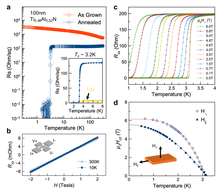
The electrical measurements were performed on samples patterned with Hall-bar geometry (see Methods, Supplementary Fig. 4). The temperature-dependent curves from 300 K to 200 mK were first acquired for both as-grown and annealed TAN films (Fig. 2a). The as-grown TAN samples showed a negative , indicating the insulating nature of the homogeneous Ti-Al-N mixture. After the annealing, an insulator-to-superconductor transition was observed with a relatively sharp phase transition temperature of 3.2 K and a sheet resistance of 132 . Comparing with the 100 nm-thick TiN parent phase deposited under the same conditions, there is a 2 orders of magnitude increase in the sheet resistance (Fig. 2a, inset). Remarkably, this observation has confirmed our hypothesis that the creation of localized Ti-rich regions in TAN spinodal systems can indeed give rise to superconductivity with significantly enhanced disorder. As a result, the sheet kinetic inductance of this 100 nm-thick TAN film given by is expected to be as large as 57 pH/, a value comparable to those observed in much thinner nitride superconductors.
A careful analysis on the temperature dependence of conductivity for the annealed TAN films revealed the material to be a disordered metal (see Supplementary Materials, Supplementary Fig. 5) [50, 51]. This is followed and confirmed by Hall resistance measurement (Fig. 2b) that yields a nearly temperature-independent carrier concentration of m-3 and an elastic mean-free-path of = 0.18 nm (corresponding to a = 1.38) under the assumption of the free-electron model (see Supplementary for more detailed discussion). To further examine the superconducting properties of the annealed TAN films, longitudinal resistance was measured under a series of magnetic fields applied both in parallel and perpendicular to the substrate surface (Fig. 2c for perpendicular field and Supplementary Fig. 6 for parallel field). The superconducting transition temperature was chosen where the longitudinal resistance was reduced by half, and the relationships between the upper critical fields and the superconducting transition temperatures () were plotted (Fig. 2d). For the parallel fields, curve can be well fitted by the Ginzburg-Landau (GL) formula and the GL coherence length was extracted to be = 7.7 nm. Owing to the fact that , where the London penetration depth for disordered superconductors is typically hundreds of nanometers [52, 53, 54], the material is confirmed to be a bulk-like, dirty type-II superconductor. While for the perpendicular fields, a deviation from the empirical GL formula was observed where the curve has an upward curvature at low fields and saturates to a higher critical fields with weaker temperature dependency (fitting details see Supplementary materials, Supplementary Fig. 6). We propose that the slight anisotropy between the parallel and perpendicular fields is caused by the existence of vertical columnar grain boundaries (see Fig. 1c,d and Supplementary Fig. 2c,d). Namely, at low fields, the columnar structures make the material resemble those granular and weakly-coupled superconductors, featuring an upward curvature in due to the change of relative magnitudes between the inter-grain coupling energy and the magnetic-flux energy [55, 56, 57]. As the field increases, the grain boundaries serve as pinning centers for the aligned vortices and enhance the superconductivity robustness [58, 59, 60]. To conclude, the phase segregation induced by spinodal decomposition in TAN results in a insulator-to-superconductor transition at around 3.2 K and a largely enhanced kinetic inductance of the material.
IV Cryogenic microwave resonator studies
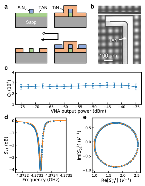
To examine the applicability of TAN for superconducting quantum circuits, we first demonstrate that the TAN system can be easily integrated into our established TiN-based processes [43]. Briefly, the TAN films were wet etched in a solution of ammonia hydroxide and hydroperoxide masked by a layer of SiNx. The etched wafers were then sent for TiN deposition without hardmask stripping. The deposited TiN layer was subsequently patterned using the SiNx-hardmask and the wet etchants (Fig. 3a, details see Methods). The eventual device structure was obtained after rinsing off the hardmask in the DHF solutions, and the scanning electron microscopy images of one exemplary device was illustrated (Fig. 3b). As given in the figures, the coplanar waveguide (CPW) resonators features a center resonator line (10 m in width, 50 m gap to ground) made of 100 nm-thick TAN films and a ground plane together with the readout feed line made of 100 nm-thick TiN films.
Cryogenic microwave studies on the CPW resonator devices were performed using a vector-network analyzer (cryogenic measurement setup see Supplementary Fig. 7). The transmission scattering parameter of the feed line was collected and the internal quality factor of the capacitively coupled TAN resonators was extracted by fitting the inverse spectra given by , where , , is the cable impedance, and is half the inverse sum of the environment impedance on the input and output sides of the resonators. Averaged quality factors of multiple resonators as a function of calculated photon numbers in the resonators were plotted (Fig. 3c), and the fitting spectra of one exemplary resonator were also provided (Fig. 3d,e). The averaged quality factor at single-photon limit is extracted to be , comparable and even better other high-kinetic-inductance resonators [17, 39, 25, 16]. In addition, the resonator quality factors were observed to have little photon-number dependency, indicating that an energy relaxation mechanism other than the well-known two-level systems (TLS) could be dominant and is under investigation for future studies. Moreover, by comparing the measured resonator frequencies with the circuit-electromagnetic simulation using HFSS (ANSYS, see Methods), it was found that the extracted surface inductance of TAN resonator is 57.4 pH/, matching well with that predicted in the transport studies. Altogether, a combination of electrical transport studies and cryogenic microwave resonator studies have all revealed the spinodal TAN system as a promising material candidate to be used for high-inductance and low-microwave-loss circuits.
V Discussions and conclusions
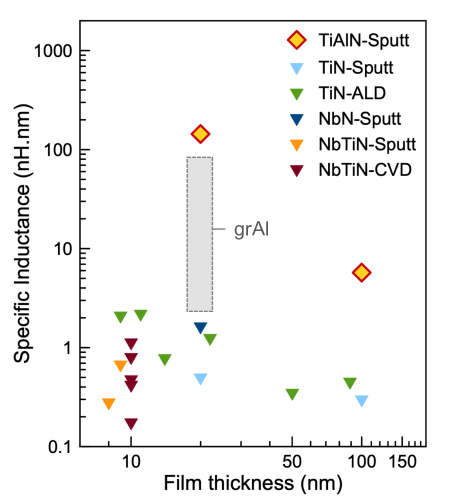
We further compare the TAN system with other reported high-kinetic-inductance material systems including a number of disordered superconducting nitrides [20, 23, 25, 18, 17, 24] and granular aluminum [16, 14, 15, 39, 40] (Fig. 4). Since it is very often the case that only sheet inductance is reported in the literatures, making it burdensome to compare materials with varied thicknesses, we use specific inductance (i.e., sheet inductance times material thickness ) to better reflect intrinsic material properties. For strongly disordered thin films with large magnetic-field penetration depth (), the specific inductance given by is essentially equivalent to the penetration depth of the materials. In the meantime, due to the fact that the penetration depth also scales with the film thickness, the specific inductance with the corresponding film thicknesses are indicated in the same plot.
For all the superconducting nitrides grown via a number of deposition techniques, the specific inductance is no greater than 3 nHnm. Although different level of chemical and structural disorder could be induced in these material systems by varying the chemical compositions and synthesis approaches, there appears to be a fundamental limit of the achievable specific inductance without the degradation of material qualities. While for spinodal TAN system with high degree of crystallinity, the 100 nm-thick films have a specific inductance of 5.7 nHnm, already higher than all the other reported ultrathin nitride materials. Again, although the specific inductance of TAN is significantly enhanced, the microwave losses as probed by CPW resonators remain low and comparable to other high-kinetic-inductance materials with much smaller specific inductance. To further examine thinner films and the potential of this material system, 20 nm-thick TAN films with the same stoichiometry were measured (Supplementary Fig. 8) and revealed a specific inductance as large as 144 nHnm (corresponding to a sheet inductance of 7.5 nH/). This value is nearly 3 orders of magnitude higher compared with the parent 20 nm-thick TiN phase and larger than many of the reported granular-aluminum systems. Given that only one representative combination of material stoichiometry and annealing condition was used in this study, it is reasonable to expect that this work has yet set any limit on the specific inductance of spinodal materials. As such, with a comprehensive engineering over the chemical compositions and phase segregation, we believe that the specific inductance of such superconducting spinodal materials could be readily tuned and controlled over a tremendously wide range.
To conclude, we have demonstrated that spinodal phase segregation in a model Ti0.48Al0.52N system can give rise to an insulator-to-superconductor transition and a drastically increased material disorder compared with the TiN parent system. The chemical and structural characterization reveal that the material remain epitaxially crystalline, while a sharp increase in the specific inductance (i.e., 2-3 orders of magnitudes larger compared with other disordered superconducting nitrides) is confirmed by both electrical transport studies and cryogenic microwave-resonator studies. To the best of our knowledge, this is the first demonstration of utilizing spinodal decomposition to trigger the insulator-to-superconductor transition with an enhanced kinetic inductance and low microwave losses. The ultrahigh kinetic inductance and good process compatibility of spinodal TAN mitigates the challenges in the engineering of low-dimension structures, making it a suitable material candidate for the development of noise-resilient superconducting qubits and high-impedance circuits. In addition, much as the large enhancement in kinetic inductance has been demonstrated in the model TAN system, similar engineering and optimization routes are in principle applicable to other spinodal systems for the investigation and optimization on materials and physical properties. This methodology, in turn, offers an unprecedented opportunity to deterministically design and engineer low-loss and high-inductance materials for advanced superconducting-quantum-circuit applications.
Acknowledgements.
We thank all members at Alibaba Quantum Laboratory for the fruitful discussions and supports. We thank the Westlake Center for Micro/Nano Fabrication and the Instrumentation and Service Center for Physical Sciences at Westlake University for the fabrication supports and the characterization services. We thank Dr. Xin Wan at Zhejiang University and Dr. Yanwei Cao at Ningbo Institute of Industrial Technology for the insightful discussions.VI Methods
Thin-film deposition. The sputter system used for this study is a CS-200 R&D type (ULVAC Inc.). The deposition chamber is equipped with a turbo-molecular pump that reaches a base-pressure of Pa. The deposition of TAN thin films was performed using a co-sputtering approach with a RF sputter gun using a 99.999% titanium target and a DC sputter gun using a 99.999% aluminum target. Before the deposition, the as-received Sapphire substrates (2-inch, single-side polished, Suzhou RDMICRO Co., Ltd.) were cleaned and heated to 300 ∘C in vacuum for dehydration. The sputter guns were then pre-sputtered with shutter closed for 60 sec to remove surface contaminants. After deposition, the samples were cooled for 10 mins and unloaded from the load-lock by venting with nitrogen.
Annealing setup. The thermal annealing was performed in a tube furnace equipped with a alumina tube and a vacuum pump. Samples were mounted in the center of the hot zone and the tube was then sealed and purged with argon (5N-purity) for at least three times. A constant flow of argon was maintained throughout the anneal at atmospheric pressure. The annealing conditions were fixed at 1000 ∘C for 30 mins.
X-ray diffractometry (XRD). The XRD studies including linescans and rocking curves were performed on a high-resolution D8 ADVANCE X-ray diffraction system (Bruker) with optics set up for epitaxial-film studies.
Transmission electron microscopy (TEM). Cross section samples were prepared with the focused ion beam (FIB) technique on an FEI Helios 650 system. The high-angle annular dark-field (HAADF) images were acquired using JEOL JEM-ARM200F electron microscope, which is equipped with a thermal field-emission gun and spherical aberration (Cs) corrector. The semi-convergence angle is around 23 mrad during HAADF imaging, and the collection angles of the detectors are 50 and 200 mrad. Energy-dispersive X-ray spectroscopy (EDX) mapping was carried out on an FEI Talos F200X TEM at 200kV equipped with a 4-inch column SDD Super-X detectors.
X-ray photo-electron spectroscopy (XPS). The XPS studies were performed on a ESCALAB Xi+ XPS system (Thermal Fisher) at an incident angle of 60 ∘. The system was first calibrated with standard samples, and the selective milling between titanium, aluminum, oxygen, and nitrogen was confirmed to be minimal. For the XPS depth-profile studies, the milling area was set to be 2 mm by 2 mm while the analyzing area was concentric with the milling area and set to be 0.4 mm by 0.4 mm. High milling current of the was applied, and the beam energy was set to 2000 eV. The spectra were taken after every milling step in a 20 sec interval for the surface region and 300 sec interval for the bulk part.
Device fabrication. The devices for transport studies were patterned into Hall-bar geometries using an established hardmask-based wet-etch approach (Supplementary Fig. 4) [43]. First, the as-grown TAN films were coated with a layer of 100 nm-thick SiNx using a Haasrode-C200A PECVD system (LEUVEN Instruments). The bi-layer stack, with lithographically patterned photoresist, was then loaded in a PlasmaPro100 ICP system (Oxford Instruments) for SiNx patterning. After the hardmask patterning and photoresist stripping, the TAN films were then wet-etched by rinsing the masked-stack in the SC-1 solution heated to 60 ∘C, which was then followed by hardmask stripping in the diluted hydrofluoric solutions (DHF). The yielded wafers were then coated with another layer of SiNx for protection over oxidation and annealed. The protective SiNx capping was stripped again in the DHF and the wafers were diced for further measurements.
For the microwave-resonators with TAN films integrated into the TiN-based quantum circuits, it is essentially a repetition of the processes discussed above. First, the TAN films was wet-etch in the SC-1 solution without stripping off the SiNx hardmask. The wet-etched wafer was subsequently rinsed in distilled water, nitrogen-blow dried, and loaded into the sputter chamber for the epitaxial-TiN deposition. The TiN deposition was performed using a 99.999% titanium target with RF sputter gun using established processes. After TiN deposition, the wafers were coated with a layer of SiNx hardmask, and was patterned similarly using the processes described above. The TiN layer was also wet-etched in the SC-1 solution, followed by hardmask stripping in the DHF solutions.
Transport studies. The transport studies were performed on patterned Hall-bar samples and the electrical connections to the sample puck were made by aluminum wedge bonding (see Fig. 2b, inset). The samples were then loaded in a physical-properties measurement system (Quantum Design Inc.) equipped with a tilting sample stage for all the subsequent characterizations. A constant current of 10 A was supplied for both longitudinal and Hall resistance measurements.
Cryogenic measurement setup. A conventional cryogenic measurement setup for the microwave resonators studies were used (Supplementary Fig. 7). The microwave signal was generated by a E5071C ENA Vector Network Analyzer (VNA, Keysight Technologies) and sent to the device under test (DUT) at the base temperature ( mK) through a series of attenuators and filters. The sample was isolated from the environment by a layer of Cu-Al shield and a layer of magnetic shield. The signal from the DUT was amplified using a high-electron-mobility transistor amplifier mounted at the 4 K-stage, and sent back to the VNA after an additional amplification at room temperature.
Electromagnetic simulation. The circuit impedance and the corresponding kinetic inductance of the superconducting materials were extracted via electromagnetic simulation using HFSS (ANSYS). The circuit model was set up based on the exact geometry of the resonator devices. By adding a continuously varied surface inductance on the resonator center line (and a known and fixed surface inductance on the TiN ground), the resonator frequencies shift towards the measured resonance frequencies until the surface inductance matches with the realistic values. The resulting surface inductance was taken as the sheet kinetic inductance of the TAN films.
References
- Manucharyan et al. [2009] V. E. Manucharyan, J. Koch, L. I. Glazman, and M. H. Devoret, Science 326, 113 (2009).
- Day et al. [2003] P. K. Day, H. G. LeDuc, B. A. Mazin, A. Vayonakis, and J. Zmuidzinas, Nature 425, 817 (2003).
- Ho Eom et al. [2012] B. Ho Eom, P. K. Day, H. G. LeDuc, and J. Zmuidzinas, Nature Physics 8, 623 (2012).
- Macklin et al. [2015] C. Macklin, K. O’Brien, D. Hover, M. E. Schwartz, V. Bolkhovsky, X. Zhang, W. D. Oliver, and I. Siddiqi, Science 350, 307 (2015).
- Earnest et al. [2018] N. Earnest, S. Chakram, Y. Lu, N. Irons, R. K. Naik, N. Leung, L. Ocola, D. A. Czaplewski, B. Baker, J. Lawrence, J. Koch, and D. I. Schuster, Physical Review Letters 120, 150504 (2018).
- Kalashnikov et al. [2020] K. Kalashnikov, W. T. Hsieh, W. Zhang, W.-S. Lu, P. Kamenov, A. D. Paolo, A. Blais, M. E. Gershenson, and M. Bell, PRX Quantum 1, 010307 (2020).
- Pechenezhskiy et al. [2020] I. V. Pechenezhskiy, R. A. Mencia, L. B. Nguyen, Y.-H. Lin, and V. E. Manucharyan, Nature 585, 368 (2020).
- Groszkowski et al. [2018] P. Groszkowski, A. D. Paolo, A. L. Grimsmo, A. Blais, D. I. Schuster, A. A. Houck, and J. Koch, New Journal of Physics 20, 043053 (2018).
- Gyenis et al. [2021a] A. Gyenis, A. Di Paolo, J. Koch, A. Blais, A. A. Houck, and D. I. Schuster, PRX Quantum 2, 030101 (2021a), arXiv:2106.10296 .
- Gyenis et al. [2021b] A. Gyenis, P. S. Mundada, A. Di Paolo, T. M. Hazard, X. You, D. I. Schuster, J. Koch, A. Blais, and A. A. Houck, PRX Quantum 2, 010339 (2021b).
- Nguyen et al. [2019] L. B. Nguyen, Y.-H. Lin, A. Somoroff, R. Mencia, N. Grabon, and V. E. Manucharyan, Physical Review X 9, 041041 (2019).
- Pop et al. [2014] I. M. Pop, K. Geerlings, G. Catelani, R. J. Schoelkopf, L. I. Glazman, and M. H. Devoret, Nature 508, 369 (2014).
- Grünhaupt et al. [2019] L. Grünhaupt, M. Spiecker, D. Gusenkova, N. Maleeva, S. T. Skacel, I. Takmakov, F. Valenti, P. Winkel, H. Rotzinger, W. Wernsdorfer, A. V. Ustinov, and I. M. Pop, Nature Materials 2019 18, 816 (2019).
- Kamenov et al. [2020] P. Kamenov, W.-S. Lu, K. Kalashnikov, T. DiNapoli, M. T. Bell, and M. E. Gershenson, Physical Review Applied 13, 054051 (2020).
- Moshe et al. [2020] A. G. Moshe, E. Farber, and G. Deutscher, Applied Physics Letters 117, 062601 (2020).
- Maleeva et al. [2018] N. Maleeva, L. Grünhaupt, T. Klein, F. Levy-Bertrand, O. Dupre, M. Calvo, F. Valenti, P. Winkel, F. Friedrich, W. Wernsdorfer, A. V. Ustinov, H. Rotzinger, A. Monfardini, M. V. Fistul, and I. M. Pop, Nature Communications 9, 1 (2018).
- Samkharadze et al. [2016] N. Samkharadze, A. Bruno, P. Scarlino, G. Zheng, D. P. DiVincenzo, L. DiCarlo, and L. M. K. Vandersypen, Physical Review Applied 5, 044004 (2016).
- Hazard et al. [2019] T. M. Hazard, A. Gyenis, A. D. Paolo, A. T. Asfaw, S. A. Lyon, A. Blais, and A. A. Houck, Physical Review Letters 122, 010504 (2019).
- Peltonen et al. [2018] J. T. Peltonen, P. C. J. J. Coumou, Z. H. Peng, T. M. Klapwijk, J. S. Tsai, and O. V. Astafiev, Scientific Reports 8, 1 (2018).
- Shearrow et al. [2018] A. Shearrow, G. Koolstra, S. J. Whiteley, N. Earnest, P. S. Barry, F. J. Heremans, D. D. Awschalom, E. Shirokoff, and D. I. Schuster, Applied Physics Letters 113, 212601 (2018).
- Knehr et al. [2021] E. Knehr, M. Ziegler, S. Linzen, K. Ilin, P. Schanz, J. Plentz, M. Diegel, H. Schmidt, E. Il’ichev, and M. Siegel, Journal of Vacuum Science & Technology A: Vacuum, Surfaces, and Films 39, 052401 (2021).
- Chand et al. [2009] M. Chand, A. Mishra, Y. M. Xiong, A. Kamlapure, S. P. Chockalingam, J. Jesudasan, V. Bagwe, M. Mondal, P. W. Adams, V. Tripathi, and P. Raychaudhuri, Physical Review B 80, 134514 (2009).
- Coumou et al. [2013a] P. C. Coumou, M. R. Zuiddam, E. F. Driessen, P. J. De Visser, J. J. Baselmans, and T. M. Klapwijk, IEEE Transactions on Applied Superconductivity 23, 10.1109/TASC.2012.2236603 (2013a).
- Hazra et al. [2018] D. Hazra, N. Tsavdaris, A. Mukhtarova, M. Jacquemin, F. Blanchet, R. Albert, S. Jebari, A. Grimm, A. Konar, E. Blanquet, F. Mercier, C. Chapelier, and M. Hofheinz, Physical Review B 97, 144518 (2018).
- Niepce et al. [2019] D. Niepce, J. Burnett, and J. Bylander, Physical Review Applied 11, 044014 (2019).
- Pita-Vidal et al. [2020] M. Pita-Vidal, A. Bargerbos, C.-K. Yang, D. J. van Woerkom, W. Pfaff, N. Haider, P. Krogstrup, L. P. Kouwenhoven, G. de Lange, and A. Kou, Physical Review Applied 14, 064038 (2020).
- Yu et al. [2021] C. X. Yu, S. Zihlmann, G. T. Fernández-Bada, J.-L. Thomassin, F. Gustavo, É. Dumur, and R. Maurand, Applied Physics Letters 118, 054001 (2021).
- Coumou et al. [2013b] P. C. J. J. Coumou, E. F. C. Driessen, J. Bueno, C. Chapelier, and T. M. Klapwijk, Physical Review B 88, 180505 (2013b).
- Tsavdaris et al. [2017] N. Tsavdaris, D. Harza, S. Coindeau, G. Renou, F. Robaut, E. Sarigiannidou, M. Jacquemin, R. Reboud, M. Hofheinz, E. Blanquet, and F. Mercier, Chemistry of Materials 29, 5824 (2017).
- Kang et al. [2011] L. Kang, B. B. Jin, X. Y. Liu, X. Q. Jia, J. Chen, Z. M. Ji, W. W. Xu, P. H. Wu, S. B. Mi, A. Pimenov, Y. J. Wu, and B. G. Wang, Journal of Applied Physics 109, 033908 (2011).
- Carbillet et al. [2016] C. Carbillet, S. Caprara, M. Grilli, C. Brun, T. Cren, F. Debontridder, B. Vignolle, W. Tabis, D. Demaille, L. Largeau, K. Ilin, M. Siegel, D. Roditchev, and B. Leridon, Physical Review B 93, 144509 (2016).
- Carbillet et al. [2020] C. Carbillet, V. Cherkez, M. A. Skvortsov, M. V. Feigel’man, F. Debontridder, L. B. Ioffe, V. S. Stolyarov, K. Ilin, M. Siegel, D. Roditchev, T. Cren, and C. Brun, Physical Review B 102, 024504 (2020).
- de Graaf et al. [2020] S. E. de Graaf, L. Faoro, L. B. Ioffe, S. Mahashabde, J. J. Burnett, T. Lindström, S. E. Kubatkin, A. V. Danilov, and A. Y. Tzalenchuk, Science Advances 6, 5055 (2020).
- Gao et al. [2008] J. Gao, M. Daal, A. Vayonakis, S. Kumar, J. Zmuidzinas, B. Sadoulet, B. A. Mazin, P. K. Day, and H. G. Leduc, Applied Physics Letters 92, 152505 (2008).
- Niepce et al. [2020] D. Niepce, J. J. Burnett, M. G. Latorre, and J. Bylander, Superconductor Science and Technology 33, 025013 (2020).
- Zhou et al. [2017] J. Zhou, J. Zhong, L. Chen, L. Zhang, Y. Du, Z. K. Liu, and P. H. Mayrhofer, Calphad 56, 92 (2017).
- To Baben et al. [2017] M. To Baben, M. Hans, D. Primetzhofer, S. Evertz, H. Ruess, and J. M. Schneider, Materials Research Letters 5, 158 (2017).
- Knutsson et al. [2013] A. Knutsson, J. Ullbrand, L. Rogström, N. Norrby, L. J. S. Johnson, L. Hultman, J. Almer, M. P. J. Jöesaar, B. Jansson, and M. Odén, Journal of Applied Physics 113, 213518 (2013).
- Zhang et al. [2019] W. Zhang, K. Kalashnikov, W.-S. Lu, P. Kamenov, T. DiNapoli, and M. Gershenson, Physical Review Applied 11, 011003 (2019).
- Valenti et al. [2019] F. Valenti, F. Henriques, G. Catelani, N. Maleeva, L. Grünhaupt, U. von Lüpke, S. T. Skacel, P. Winkel, A. Bilmes, A. V. Ustinov, J. Goupy, M. Calvo, A. Benoît, F. Levy-Bertrand, A. Monfardini, and I. M. Pop, Phys. Rev. Applied 11, 054087 (2019).
- Xia et al. [1998] Q. Xia, H. Xia, and A. L. Ruoff, Journal of Applied Physics 73, 8198 (1998).
- Camp et al. [1991] P. E. V. Camp, V. E. V. Doren, and J. T. Devreese, Physical Review B 44, 9056 (1991).
- Gao et al. [2021] R. Gao, W. Yu, H. Deng, H.-S. Ku, Z. Li, M. Wang, X. Miao, Y. Lin, and C. Deng, Epitaxial titanium nitride microwave resonators: Structural, chemical, electrical, and microwave properties (2021), arXiv:2111.04227 [quant-ph] .
- Höglund et al. [2010] C. Höglund, B. Alling, J. Birch, M. Beckers, P. O. Å. Persson, C. Baehtz, Z. Czigány, J. Jensen, and L. Hultman, Physical Review B 81, 224101 (2010).
- Calamba et al. [2019a] K. M. Calamba, J. F. Pierson, S. Bruyère, A. L. Febvrier, P. Eklund, J. Barrirero, F. Mücklich, R. Boyd, M. P. J. Jõesaar, and M. Odén, Journal of Applied Physics 125, 105301 (2019a).
- Calamba et al. [2021] K. M. Calamba, J. Salamania, M. P. Jõesaar, L. J. Johnson, R. Boyd, J. F. Pierson, M. A. Sortica, D. Primetzhofer, and M. Odén, Acta Materialia 203, 116509 (2021).
- Chaar et al. [2021] A. B. Chaar, L. Rogström, M. P. Johansson-Jöesaar, J. Barrirero, H. Aboulfadl, N. Schell, D. Ostach, F. Mücklich, and M. Odén, Journal of Alloys and Compounds 854, 157205 (2021).
- Calamba et al. [2019b] K. M. Calamba, J. Barrirero, M. P. Jõesaar, S. Bruyère, R. Boyd, J. F. Pierson, A. Le Febvrier, F. Mücklich, and M. Odén, Thin Solid Films 688, 137414 (2019b).
- Greczynski et al. [2019] G. Greczynski, L. Hultman, and M. Odén, Surface and Coatings Technology 374, 923 (2019).
- Kaveh and Mott [1982] M. Kaveh and N. F. Mott, Journal of Physics C: Solid State Physics 15, L707 (1982).
- Lee and Ramakrishnan [1985] P. A. Lee and T. V. Ramakrishnan, Reviews of Modern Physics 57, 287 (1985).
- Qiao et al. [2018] L. Qiao, D. Li, S. V. Postolova, A. Y. Mironov, V. Vinokur, and B. Rosenstein, Scientific Reports 8, 1 (2018).
- Diener et al. [2012] P. Diener, H. Schellevis, and J. J. A. Baselmans, Applied Physics Letters 101, 252601 (2012).
- Pracht et al. [2012] U. S. Pracht, M. Scheffler, M. Dressel, D. F. Kalok, C. Strunk, and T. I. Baturina, Physical Review B 86, 184503 (2012).
- Deutscher and Entin-Wohlman [1978] G. Deutscher and O. Entin-Wohlman, Physical Review B 17, 1249 (1978).
- Deutscher et al. [1980] G. Deutscher, O. Entin-Wohlman, and Y. Shapira, Physical Review B 22, 4264 (1980).
- Klemm et al. [1975] R. A. Klemm, A. Luther, and M. R. Beasley, Physical Review B 12, 877 (1975).
- Jung et al. [2012] S.-G. Jung, W. K. Seong, and W. N. Kang, Journal of Applied Physics 111, 053906 (2012).
- Matsumoto and Mele [2009] K. Matsumoto and P. Mele, Superconductor Science and Technology 23, 014001 (2009).
- Durrell et al. [2011] J. H. Durrell, C.-B. Eom, A. Gurevich, E. E. Hellstrom, C. Tarantini, A. Yamamoto, and D. C. Larbalestier, Reports on Progress in Physics 74, 124511 (2011).