Optical and dielectric properties of MoO3 nanosheets for van der Waals heterostructures
Abstract
Two-dimensional (2D) insulators are a key element in the design and fabrication of van der Waals heterostructures. They are vital as transparent dielectric spacers whose thickness can influence both the photonic, electronic, and optoelectronic properties of 2D devices. Simultaneously, they provide protection of the active layers in the heterostructure. For these critical roles, hexagonal Boron Nitride (hBN) is the dominant choice due to its large bandgap, atomic flatness, low defect density, and encapsulation properties. However, the broad catalogue of 2D insulators offers exciting opportunities to replace hBN in certain applications that require transparent thin layers with additional optical degrees of freedom. Here we investigate the potential of single-crystalline Molybdenum Oxide (MoO3) as an alternative 2D insulator for the design of nanodevices that require precise adjustment of the light polarization at the nanometer scale. First, we measure the wavelength-dependent refractive indices of MoO3 along its three main crystal axes and determine the in-plane and out-of-plane anisotropy of its optical properties. We find the birefringence in MoO3 nanosheets compares favorably with other 2D materials that exhibit strong birefringence, such as black phosphorus, ReS2, or ReSe2, in particular in the visible spectral range where MoO3 has the unique advantage of transparency. Finally, we demonstrate the suitability of MoO3 for dielectric encapsulation by reporting linewidth narrowing and reduced inhomogeneous broadening of 2D excitons and optically active quantum emitters, respectively, in a prototypical monolayer transition-metal dichalcogenide semiconductor. These results show the potential of MoO3 as a 2D dielectric layer for manipulation of the light polarization in vertical 2D heterostructures.
The remarkable diversity of van der Waals (vdW) layered crystals, the breadth of their properties, and the ability to stack them without restriction has positioned atomically-thin crystals as a unique platform to develop novel heterostructure-based devices with engineered functionalities Geim and Grigorieva (2013). A key ingredient in the design of vdW heterostructures for electronic and photonic applications is an insulator: a transparent layered dielectric material to encapsulate the active material for both protection and device functionality. Among the broad catalog of wide-bandgap materials offered by the vdW family, high-quality hexagonal Boron Nitride (hBN) is the dominant choice due to its atomic flatness and low defect density. Encapsulation of graphene or transition metal dichalcogenides (TMDs) with hBN can significantly reduce environmental disorder Rhodes et al. (2019) to yield significantly enhanced transport Dean et al. (2010); Bandurin et al. (2017) and optical Cadiz et al. (2017); Ajayi et al. (2017); Wierzbowski et al. (2017) properties. In addition, hBN is an invaluable dielectric spacer for engineering the optical properties Gerber and Marie (2018); Brotons-Gisbert et al. (2018); Fang et al. (2019); Raja et al. (2017); Unuchek et al. (2019) and can act as a tunnel barrier between active 2D regions Brotons-Gisbert et al. (2019); Shimazaki et al. (2020); Pan et al. (2018) with a tunnelling probability that can be precisely controlled by the number of atomic layers Britnell et al. (2012). While hBN is ubiquitous due to these exceptional properties, some drawbacks exist. High-purity hBN is typically obtained only in extreme conditions Watanabe, Taniguchi, and Kanda (2004), creating scarcity. Further, the nuclear spins of all isotopes of both boron and nitrogen are non-zero Rumble (1992); Stone (2014). Suppl. Table S1 presents the nuclear spin number (I) and natural abundance for each isotope of boron and nitrogen. A zero nuclear spin number can only be obtained when both atomic numbers Z and A are even for all atoms in a material, a requirement that hBN fails to meet. For some applications in quantum information science, this leads to spin decoherence, as observed in magnetic resonance spectroscopy of atomically thin hBN Lovchinsky et al. (2017). This can negatively affect the spin coherence of an electron localized at a lattice defect Gottscholl et al. (2020) or a quantum dot encapsulated by hBN Brotons-Gisbert et al. (2019); Baek et al. (2020); Klein et al. (2021).
Beyond a passive role as an isotropic dielectric material, an insulating vdW material that can protect the active region of a heterostructure and play additional roles in the device functionality provides new opportunities. For instance, due to the extreme sensitivity of excitons in 2D materials such as monolayer (ML) transition metal dichalcogenides (TMDs) to their environment, it is possible to control and tune the electronic and optical properties (such as the bandgap and exciton binding energies) using dielectric engineering techniques Raja et al. (2017). Further, specific hBN thicknesses can be chosen for particular applications to optimise specific characteristics, e.g., to engineer the far-field radiation pattern Brotons-Gisbert et al. (2018) or to control the tunnel barrier for carriers and interlayer coupling Gerber and Marie (2018); Brotons-Gisbert et al. (2019); Shimazaki et al. (2020). But, in the case of hBN, its refractive index is isotropic within the exfoliation plane making thickness the only variable to control in the heterostructure design. In this context, in-plane anisotropic insulators could offer a new knob to tune the dielectric properties. This degree of freedom could prove valuable for next-generation optoelectronic, photonic, and quantum devices.
In this framework, an intriguing alternative to hBN is single-crystalline MoO3. MoO3 has a relatively large indirect bandgap (> 3 eV Hussain and Rao (2003); Balendhran et al. (2013)), ideal for applications requiring a transparent material in the visible and near-infrared part of the spectrum. For example, MoO3 has been used in silicon Geissbühler et al. (2015), perovskite Zhao, Nardes, and Zhu (2014), and organic Tseng et al. (2012) photovoltaics applications and as a buffer layer in organic light-emitting diodes Shin et al. (2008). Moreover, the dominant isotopes of both molybdenum and oxygen have zero nuclear spins (see Suppl. Table S1), positioning MoO3 as a promising candidate for applications that require spin coherence. In addition, MoO3 presents an in-plane anisotropic crystal structure in its layered phase (-MoO3) Zhang, Qu, and Lai (2017); Molina-Mendoza et al. (2016); Wei et al. (2020), enabling a platform for ultra-low-loss polaritons due to anisotropy Ma et al. (2018) and anisotropic phonon-polariton propagation along the surface of a rotated MoO3 bilayer Hu et al. (2020). Similar crystal anisotropies have been exploited to fabricate optical and optoelectronic devices Yuan et al. (2015); Wang et al. (2017); Yang et al. (2017), positioning MoO3 as a candidate for nanodevices in which transparent thin layers with an additional tunable variable are needed. Although the dielectric properties of single-crystal bulk -MoO3 and its biaxial optical anisotropy have been measured by valence electron-energy-loss spectroscopy Lajaunie et al. (2013) and interferometric methods Deb (1968), the wavelength-dependent in-plane and out-of-plane birefringence of single-crystalline MoO3 nanoflakes and the performance MoO3 as an encapsulation dielectric for vdW heterostructures has not yet been investigated.
Here, we characterize the optical and encapsulating properties of MoO3 nanosheets. First, using an imaging ellipsometer, we measure the refractive indices along the a, b, and c axes and determine the in-plane and out-of-plane wavelength-dependent birefringence of the refractive indices for MoO3. To unambiguously demonstrate the in-plane anisotropy, we measure the polarization dependent reflectivity of a MoO3 nanosheet and observe the effective refractive index is dependent on the incident polarization. Building on these results, we calculate the optical phase retardance as a function of sample thickness and wavelength of these MoO3 nanosheets. Finally, we apply MoO3 as an encapsulating material for a ML WSe2 layer. We probe the absorption at cryogenic temperatures of the WSe2 A-exciton and, relative to a reference unencapsulated ML WSe2 sample, observe substantial linewidth narrowing and an energetic blue-shift. We ascribe this improvement to the atomic flatness, reduced disorder, and dielectric environment of the MoO3. Further, we characterize a single quantum emitter in the MoO3 encapsulated WSe2, and observe linewidths on par with those observed in hBN encapsulated WSe2. The performance of MoO3 as an encapsulation dielectric is found to be comparable to hBN. Overall, we find the intrinsic anisotropy of the optical properties of MoO3 provides an unexplored degree of freedom useful for photonic applications while simultaneously MoO3’s dielectric properties suggest its suitability as a candidate to replace hBN in certain applications.
We prepare MoO3 nanosheets via mechanical exfoliation from bulk crystals (2DSemiconductors, Scottsdale, AZ, USA) in an Ar environment. The thickness of the exfoliated nanosheets is estimated in situ by optical contrast analysis (see Suppl. Figure S1), a reliable and accurate method to characterize the thickness of 2D materials Brotons-Gisbert et al. (2017); Krečmarová et al. (2019), including MoO3 Puebla et al. (2020). The MoO3 nanosheets employed as encapsulating layers in our vertical vdW heterostructures are 15 - 40 nm thick, while the MoO3 layers studied via ellipsometry and differential reflectivity measurements are 110 - 150 nm thick.
Assembly of heterostructures incorporating WSe2 (2DSemiconductors, Scottsdale, AZ, USA) were carried out using the hot pick-up transfer technique Pizzocchero et al. (2016) in the inert environment to promote pristine interfaces. Spectroscopic ellipsometry measurements were carried out using a spectroscopic imaging (spatial resolution 1 m) nulling ellipsometer (EP4, Accurion Gmbh, Göttingen, Germany) in an Ar atmosphere at room temperature in the wavelength range from 410 nm to 980 nm with constant wavelength steps of 10 nm. Optical reflectance and photoluminescence (PL) spectroscopy measurements were carried out at T=4K using a diffraction limited confocal microscope.
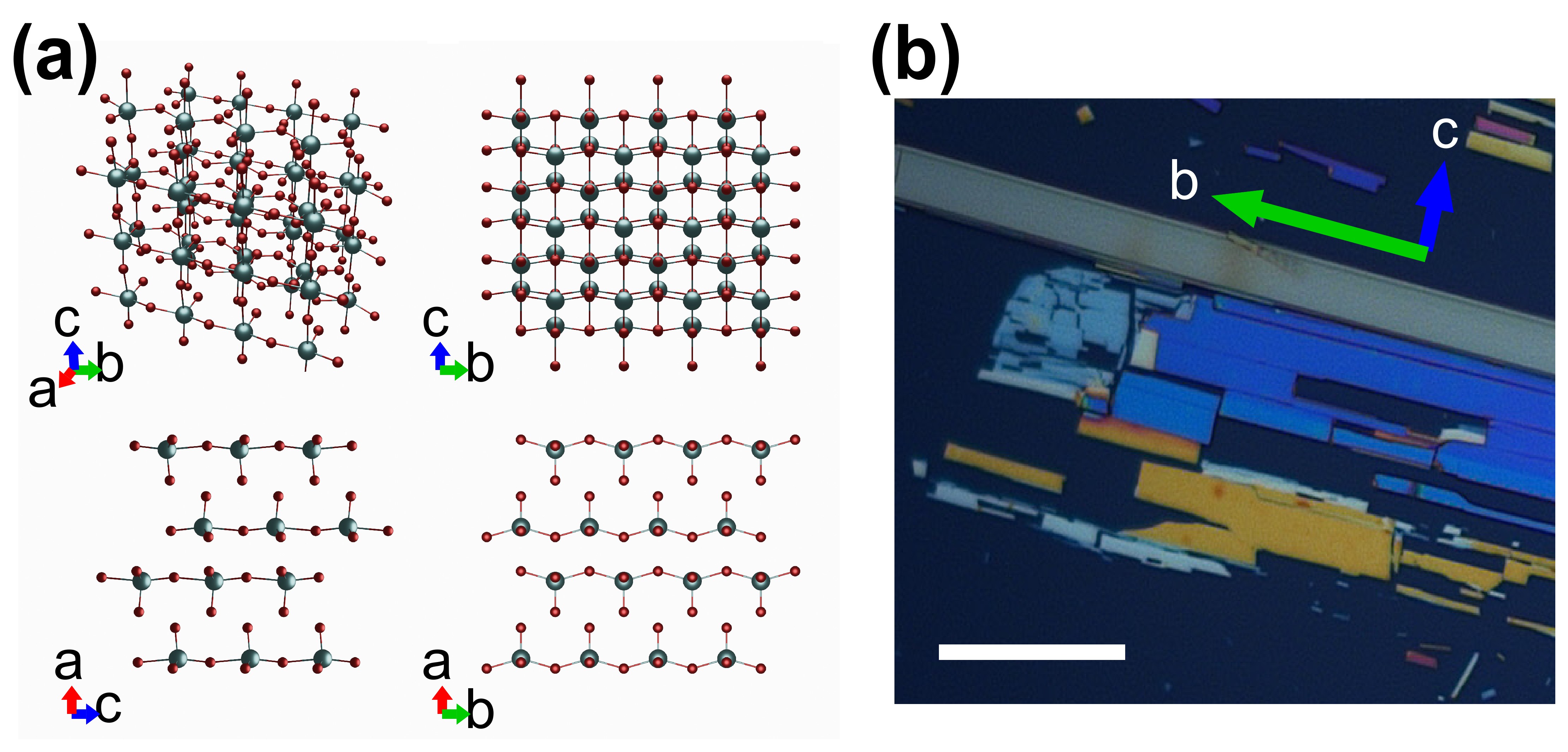
- MoO3, with a centrosymmetric Pnma (62) structure Kim et al. (2019); Yao et al. (2012) as shown in Figure 1(a), is the thermally stable phase of MoO3. It has a laminar structure with lattice parameters Å, Å and Å () Lajaunie et al. (2013); Kim et al. (2019). Mo - O bonding within each layer is covalent whereas bonding between layers is of vdW type, making possible its exfoliation (Figure 1(b)). However, within the in-plane crystallographic directions, a drastic difference in bond strength can be observed both in Figure 1(a), comparing views from and axis, and in Figure 1(b), which reveals clear rectangular shapes. The directions defined by different bonding strengths make it possible to identify the direction parallel to longer sides (higher bond density) and shorter ones (weaker bond density) with and directions, respectively, while is the out-of-plane direction.
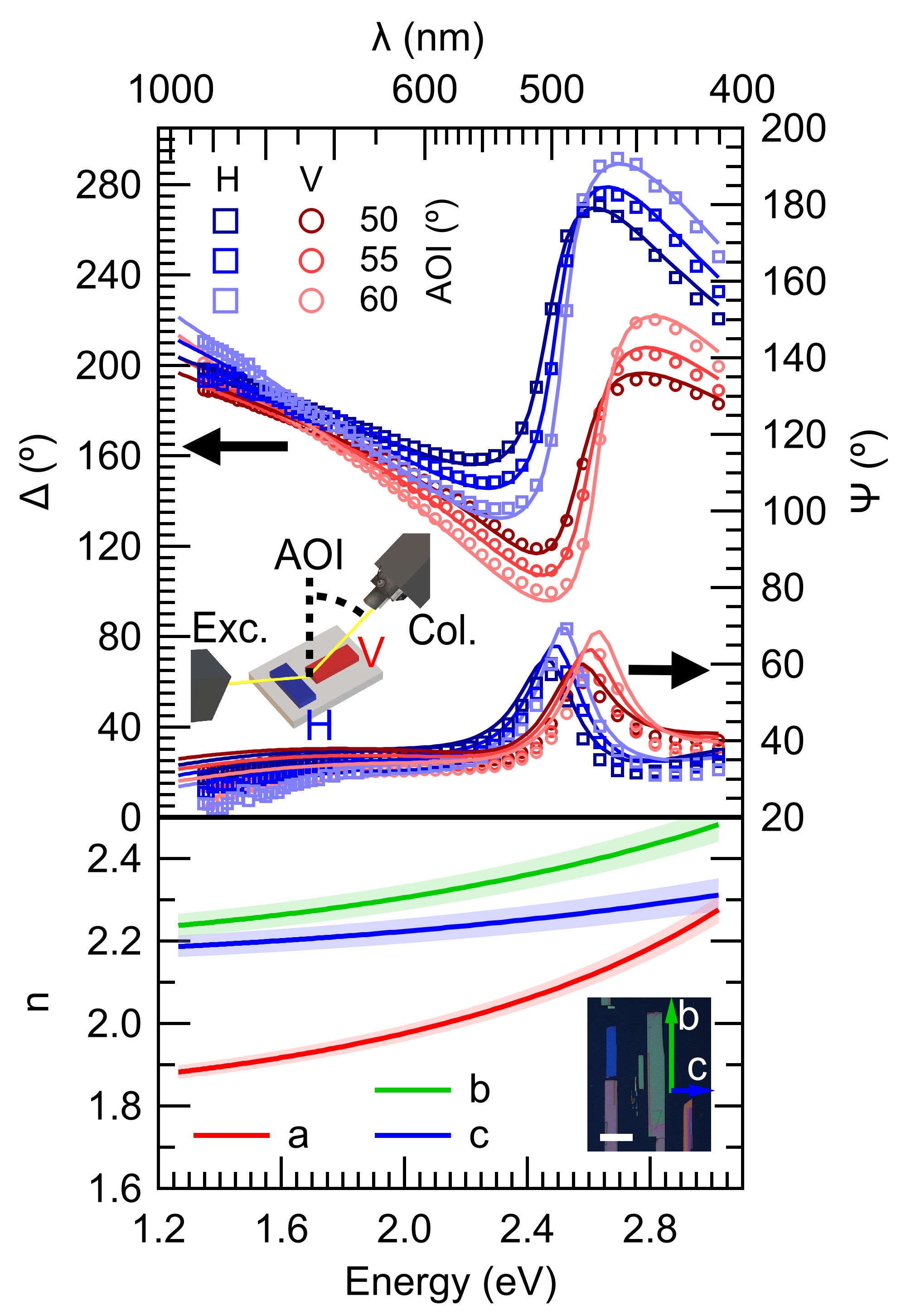
To probe and directly correlate the optical properties with crystal anisotropy, we perform imaging spectroscopic ellipsometry of MoO3 samples. Figure 2, top panel, shows the ellipsometric angles and (open circles and squares) measured for a 112 nm thick MoO3 nanosheet on a Si/SiO2 substrate. Ellipsometric data from the samples were acquired at three different angles of incidence (defining the vertical as ) in five-degree steps and two orthogonal incidence planes obtained via two sets of measurements taken by rotating the samples in the azimuthal angle = 90∘ within the - plane (in-plane). In this scenario, the wave vector of the excitation beam is contained within the - crystallographic plane (labeled as H configuration, in blue tones, when the longer side of the nanosheets – crystallographic direction– is perpendicular to the direction described by the incidence and nanosheet planes) or within the - plane (labeled as V configuration, in red tones, when the longer side of the nanosheets – crystallographic direction– is parallel to the direction described by the incidence and nanosheet planes). For a quantitative analysis of the optical properties of the MoO3 nanosheet it is necessary to fit the measured data with an appropriate multilayer model. With the aim of minimizing substrate-induced uncertainties in the determination of the refractive index of MoO3 flakes, ellipsometric data from the bare Si/SiO2 substrate were also measured simultaneously on a spot very close to the MoO3 nanosheet using the same experimental conditions. Suppl. Figure S2 shows the ellipsometric angles and measured for the bare Si/SiO2 substrate, from which an oxide thickness of 97.3 0.1 nm was determined by employing the reported refractive indices of Si and SiO2 Henrie et al. (2004). Due to the strong crystal anisotropy of MoO3, we modelled its refractive index as a biaxial birefringent medium, where , and are the refractive indices along each crystal axis. Because the extinction coefficients for MoO3 in the visible range are very low Puebla et al. (2020), we neglect that term in our model and assume real-valued refractive indices described by a Sellmeier dispersion law of the form , with . The solid lines in the top panel in Figure 2 represent numerical fits of the experimental data to our theoretical model, from which the refractive indices along the different crystallographic axes are obtained (see the bottom panel in Figure 2). The good agreement between the experimental values and the theoretical fits verifies that our assumption of real-valued refractive indices for MoO3 nanoflakes in the visible range is reasonable. The Sellmeier coefficients resulting from the numerical fits are summarized in Suppl. Table S2. As can be seen in the bottom panel in Figure 2, the refractive index of MoO3 nanosheets presents a clear biaxial anisotropy, with values of , and in good agreement with previously reported values for single-crystalline bulk MoO3 Deb (1968) and a recent study on MoO3 nanosheets Puebla et al. (2021). The results in Figure 2 also highlight a large in-plane/out-of-plane birefringence in MoO3 for visible wavelengths. At = 633 nm we measure and , which are higher in absolute value than the values found in other birefringent crystals such as YVO4 ( at 633 nm Shi, Zhang, and Shen (2001)) which is widely used in laser devices and optical components.
In addition to the in-plane/out-of-plane birefringence, MoO3 nanosheets also show a marked in-plane birefringence, for instance at 520 nm. Although smaller than the in-plane birefringence of black phosphorus ( at 520 nm Yang et al. (2017), birefringence that has been recently explored for its potential use in reconfigurable color displays Jia et al. (2021)), the measured in-plane birefringence for MoO3 is 3 times larger than that of other vdW materials such as ReS2 (0.037 Yang et al. (2017)) and ReSe2 (0.047Yang et al. (2017)) at 520 nm, and is comparable to that of state-of-the-art bulk birefringent materials such as CaCO3 (0.17Yang et al. (2017)). However, unlike the previously mentioned vdW materials with large in-plane birefringence, MoO3 is transparent in the visible spectral range Puebla et al. (2021), opening this feature to applications where a transparent material is necessary. Such in-plane birefringence positions MoO3 as an ideal candidate for polarization-integrated vdW nanodevices that require precise adjustment of the light polarization at the nanometer scale. The electric field components of a plane wave propagating along the axis of MoO3 with a linear polarization state misaligned with respect to the and crystallographic axes experience a phase retardance given by , with being the MoO3 thickness. Since the band structure of MoO3 has a negligible thickness dependence Molina-Mendoza et al. (2016), we do not expect the refractive index to depend on the nanosheet thickness. Therefore, for a given the phase retardance grows linearly with the sample thickness. Given that the ML thickness of MoO3 is 0.7 nm Cai et al. (2017), we estimate a maximum phase retardance of per atomic layer at 410 nm. Suppl. Figure S3 shows the calculated phase retardance induced by MoO3 as a function of the sample thickness and light wavelength.
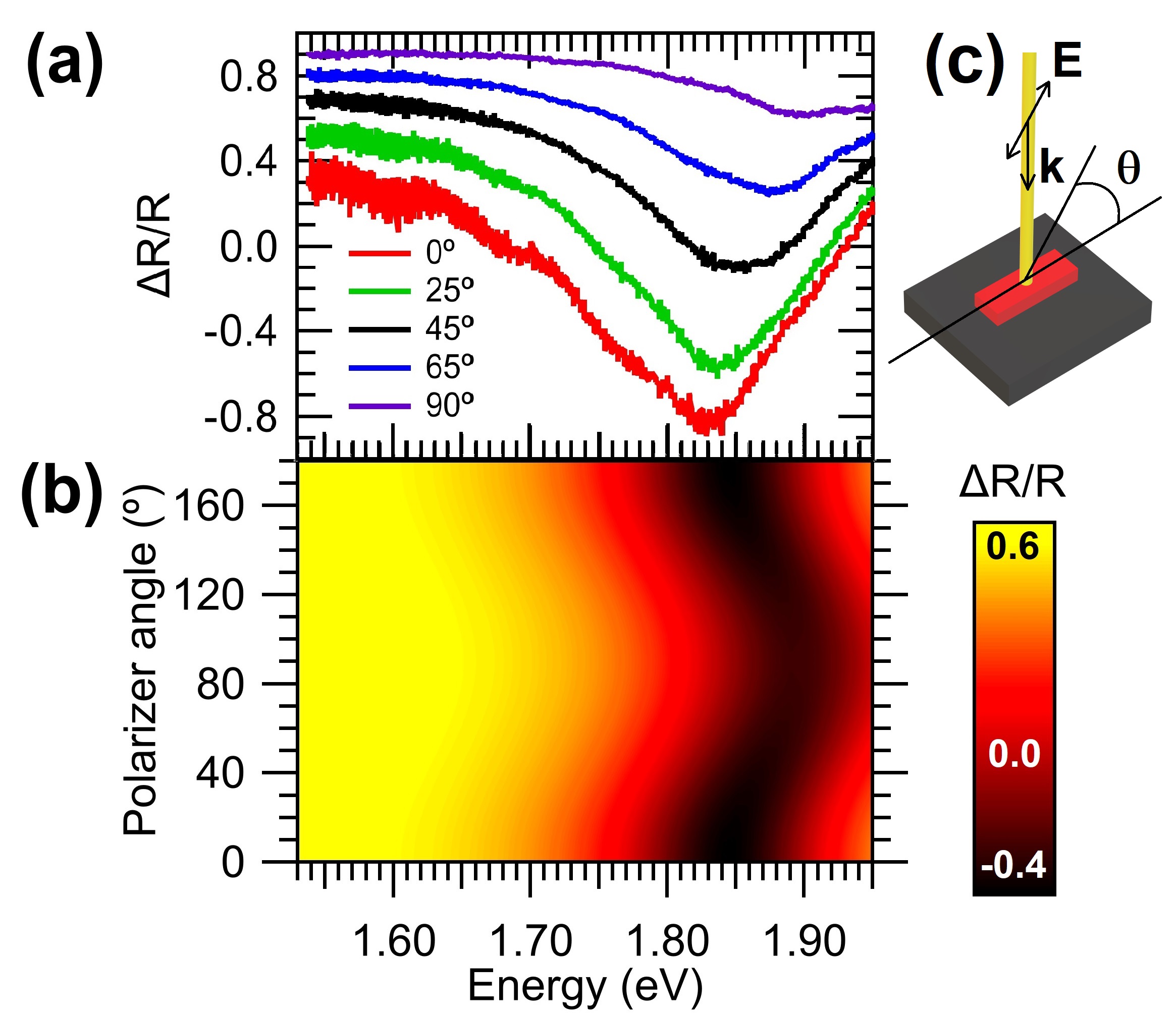
To further show the role that the in-plane anisotropy of MoO3 can play in the design of nanodevices for photonics applications, we perform linear-polarization-resolved optical reflectance spectroscopy measurements in MoO3 samples exfoliated on top of a Si/SiO2 substrate. During the measurements, the azimuthal angle of the linearly polarized incident light is rotated with respect to the crystallographic in-plane axes of MoO3 with steps of 5 degrees in a vertical diffraction limited confocal microscope with normal incidence (). Figure 3(a) shows linear reflectance contrast spectra () acquired for a MoO3 nanosheet under different incident angles, where and represent incident linearly-polarized light aligned with the and axis, respectively. The linear reflectance contrast spectra were calculated as , with and the reflectivity measured in the sample and the bare substrate, respectively. The spectra show clear minima that blueshift when the incident light is rotated from parallel to the axis to parallel to the , in addition to an overall intensity change. The origin of such minima can be attributed to the destructive interference enabled by the optical thickness of MoO3, for which the reflected intensity becomes minimum at a wavelength , with being the MoO3 thickness, being an effective in-plane refractive index, and being the order of the interference maximum. Due to the in-plane anisotropy of MoO3, the incident polarized light experiences a different refractive index which depends on the azimuthal angle through the equation:
| (1) |
which states that the optical thickness for which the constructive interference is satisfied depends on the azimuthal angle of the incident light. This result yields a redshift of the wavelength of the minimum as the incident angle is rotated from to . Figure 3(b) shows the calculated of a nm MoO3 nanosheet on top of a Si/SiO2 substrate with an oxide layer of 97 nm as a function of the incident angle. The calculations were carried out using a multilayer transfer matrix using the in-plane refractive indices shown in Figure 2. These results not only reproduce the observed blueshift of the minima but also account for the observed intensity change of the as function of the illumination angle.
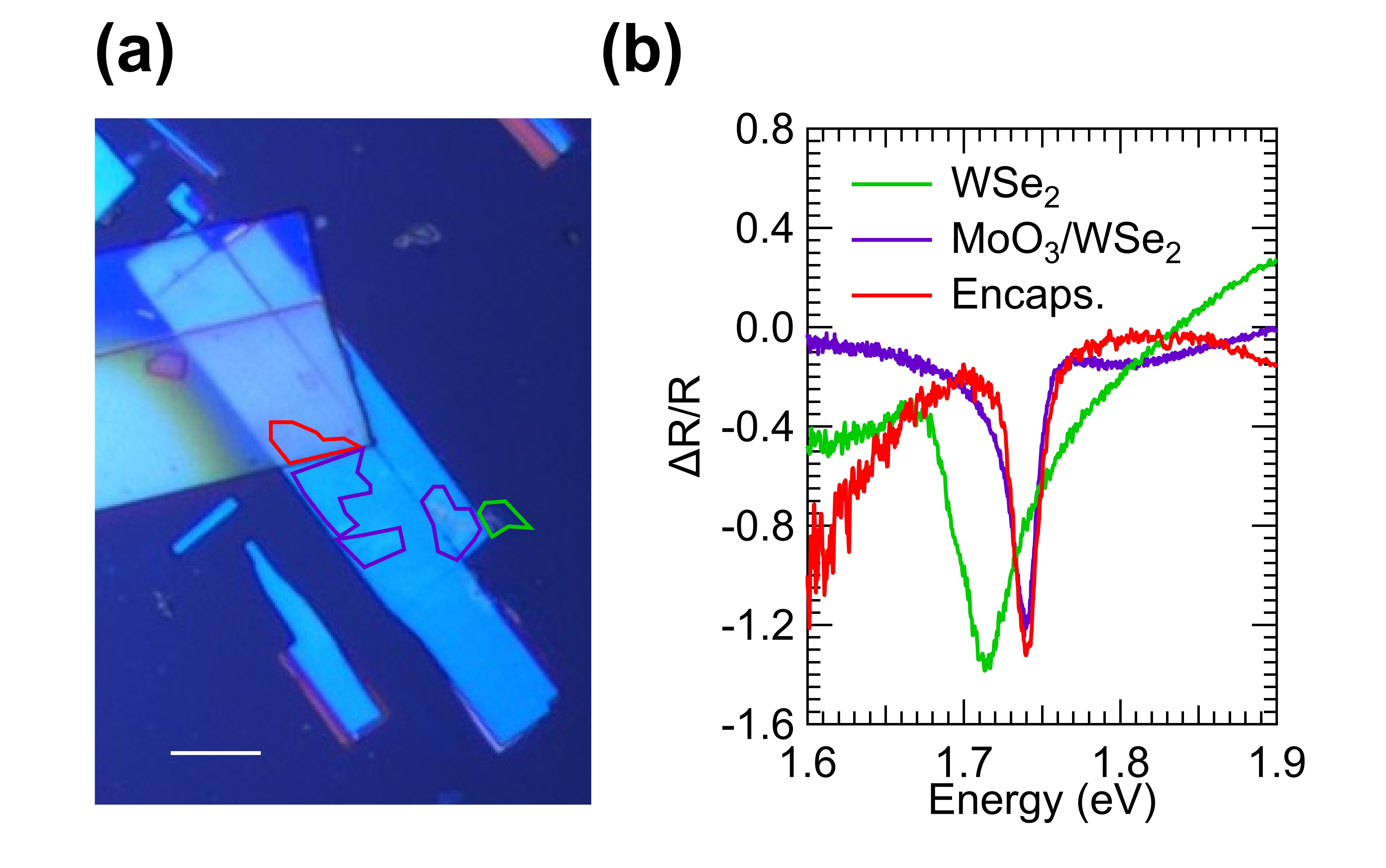
Next, to investigate the potential of MoO3 as a dielectric spacer and encapsulating layer for vdW heterostructure devices, we fabricated a sample consisting of a ML WSe2 partially encapsulated by MoO3 on top of a Si/SiO2 (90 nm) substrate. Figure 4(a) shows an optical image of the fabricated heterostructure, in which three different regions can be identified: i) a region where the WSe2 ML lays directly on top of the Si/SiO2 substrate (area outlined in green); ii) a region where the WSe2 ML is separated from the Si/SiO2 substrate by a bottom MoO3 layer (purple area); and iii) a region where the WSe2 ML is fully encapsulated by top and bottom MoO3 layers (red area). Figure 4(b) shows low-temperature (LT) spectra measured at the spatial positions indicated in Figure 4(a) in the energy range 1.6-1.9 eV. In this spectral region, the fundamental direct optical transition (so-called A-excitons at the and points of the hexagonal Brillouin zone) dominates the optical response of the WSe2 ML. We observe the WSe2 exciton resonances in the partially (purple) and fully encapsulated (red) regions show a pronounced shift of 26 meV to higher energies as compared to the WSe2 on SiO2. Energy shifts of similar magnitude have also been observed for WSe2 and other 2D TMDs deposited on top of different substrates and encapsulated by hBN or layers with different refractive indices Lin et al. (2014); Stier et al. (2016); Raja et al. (2017, 2019); Steinleitner et al. (2018). The observed energy shifts are the result of the local dielectric screening of the Coulomb interactions induced by the dielectric surroundings of the 2D layers Lin et al. (2014); Raja et al. (2017, 2019); Steinleitner et al. (2018), which leads to substantial and opposite shifts of the free-carrier bandgap and the exciton binding energy . Although for encapsulated samples both magnitudes might change considerably, in our experiments we only can access the exciton energy (i.e. the difference between and ). Therefore, the resulting energy shift (either to higher or lower energies), is the result of the relative energy shifts and , which typically give rise to a very small shift compared to the exciton energy in non-encapsulated samples. In our case, the observed energy blueshift for the exciton resonance indicates that . Moreover, the observed energy shift of the exciton resonance is accompanied by a substantial narrowing of the exciton linewidth for the partially and fully encapsulated regions of the sample ( meV) as compared to the non-encapsulated one ( meV). Similar narrowing of exciton linewidths, attributed to a reduction of the inhomogeneous broadening, has also been observed for different ML TMDs encapsulated by hBN as a consequence of protection from possible substrate-related charge and electric field fluctuations as well as increased flatness enabled by the hBN encapsulation Cadiz et al. (2017); Ajayi et al. (2017). Although linewidths approaching the homogeneous limit (as narrow as 2 meV) have been reported, the exciton linewidths we measure for WSe2 encapsulated by MoO3 are very similar to the ones we routinely obtain for hBN-encapsulated WSe2 (see Suppl. Figure S4). Further improvements could be possible with higher purity WSe2 crystals Edelberg et al. (2019) and incorporation into electrostatically gated devices. These results confirm that MoO3 represents an alternative to hBN as a dielectric spacer and protecting layer for vdW-based heterostructure devices.
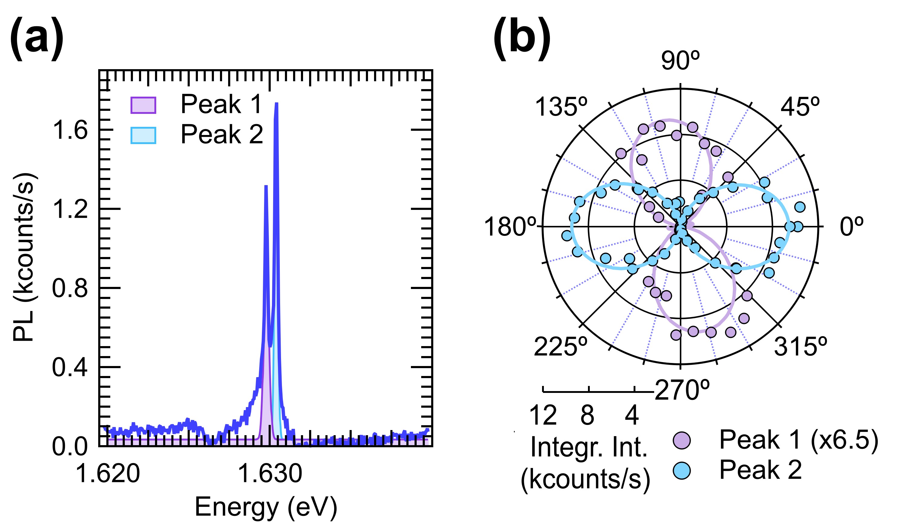
Finally, motivated by potential applications for MoO3 in quantum devices, we investigate the effect MoO3 encapsulation has on the properties of quantum emitters in ML WSe2. Confocal PL imaging of several bare MoO3 flakes at a temperature of 4K confirms the absence of LT emission from MoO3 in the energy range 1.55-1.95 eV. Conversely, confocal PL scanning of MoO3-encapsulated ML WSe2 reveals a few localized spots with higher PL intensity than the homogeneous emission background. These localized bright spots present discrete spectrally narrow peaks originating from WSe2 quantum emitters Brotons-Gisbert et al. (2019); Srivastava et al. (2015); He et al. (2015); Tonndorf et al. (2015); Kumar, Kaczmarczyk, and Gerardot (2015). Figure 5(a) shows a PL spectrum of the neutral exciton of a single WSe2 quantum emitter fully encapsulated in MoO3. The spectrum exhibits a clear doublet, split by eV, with orthogonally linear polarized emission, as shown in Figure 5(b). The emission doublet is a fine-structure splitting arising from the electron–hole exchange interaction energy and the asymmetry in the confinement potential Srivastava et al. (2015); He et al. (2015); Tonndorf et al. (2015); Brotons-Gisbert et al. (2019); Kumar, Kaczmarczyk, and Gerardot (2015). The fine-structure doublet exhibits the typical saturation behavior of a single quantum emitters with increasing power, as shown in Suppl. Figure S5. The individual fine-structure split peaks exhibit emission linewidths of 150 and 230 eV and minimal spectral fluctuation at long timescales. Over 10 minutes, the standard deviation of the peak energy is 20 eV (see Suppl. Figure S6). Overall, the inhomogeneous broadening of the WSe2 quantum emitters fully encapsulated in MoO3 is comparable to those fully encapsulated in hBN Brotons-Gisbert et al. (2019).
In summary, we have demonstrated that MoO3 is a viable alternative to hBN as a 2D dielectric insulator, in particular for quantum devices requiring spin coherence or applications requiring an extra degree of freedom to fine-tune photonic heterostructures due its in-plane birefringence. We report the refractive indices along the three crystal axes of MoO3 and find that the in-plane birefringence of MoO3 is among the highest reported for a 2D material. These results are complemented by differential reflectivity measurements. As an example advantage of its unusually high birefringence, MoO3’s potential use as an optical phase retardance element is proposed. Finally, we demonstrated the suitability of MoO3 nanosheets for dielectric encapsulation, reporting linewdith narrowing in ML WSe2 and reduced inhomogeneous broadening of optically active TMD quantum emitters. These results pave the way for MoO3 as a dielectric element for vertical vdW heterostructures.
Supplementary Material
The following are available online. Table S1: Nuclear spin number (I) and abundance in nature of hBN and MoO3 constituents: Boron, Nitrogen, Oxygen and Molybdenum, Figure S1: Optical contrast analysis for MoO3 nanosheets thickness identification, Figure S2: Ellipsometry and (circled dots) measured on the bare Si/SiO2 substrate, Table S2: Sellmeier coefficients resulting from the numerical fits in a dispersion law of the form , with being the axes in MoO3 nanoflakes described in Figure 2, Figure S3: Calculated phase retardance induced by a MoO3 nanosheet as a function of the sample thickness and light wavelength, Figure S4: Typical in WSe2 monolayer encapsulated in hBN at LT, showing a narrowing similar to the obtained in MoO3 encapsulated WSe2 monolayer in Figure 4, Figure S5: Fine structure splitting power dependence in LT emitters in an encapsulated WSe2 ML on MoO3, Figure S6: Jittering in the emitter in a WSe2 ML encapsulated in MoO3 described in Figure 5
Acknowledgements.
This work is supported by the EPSRC (grant no. EP/P029892/1), the ERC (grant no. 725920) and the EU Horizon 2020 research and innovation program under grant agreement no. 820423. B.D.G. is supported by a Wolfson Merit Award from the Royal Society and a Chair in Emerging Technology from the Royal Academy of Engineering. M.B.-G. is supported by a Royal Society University Research Fellowship. D.A.-P. acknowledges fellowship no. UV-INV-PREDOC17F1-539274 under the program "Atracció de Talent, VLCCAMPUS" of the University of Valencia for its funding through a research stay.Data Availability Statement
The data that support the findings of this study are available from the corresponding author upon reasonable request.
References
- Geim and Grigorieva (2013) A. K. Geim and I. V. Grigorieva, “Van der Waals heterostructures,” Nature 499, 419–425 (2013).
- Rhodes et al. (2019) D. Rhodes, S. H. Chae, R. Ribeiro-Palau, and J. Hone, “Disorder in van der Waals heterostructures of 2D materials,” Nature Materials 18, 541–549 (2019).
- Dean et al. (2010) C. R. Dean, A. F. Young, I. Meric, C. Lee, L. Wang, S. Sorgenfrei, K. Watanabe, T. Taniguchi, P. Kim, K. L. Shepard, et al., “Boron nitride substrates for high-quality graphene electronics,” Nature Nanotechnology 5, 722–726 (2010).
- Bandurin et al. (2017) D. A. Bandurin, A. V. Tyurnina, L. Y. Geliang, A. Mishchenko, V. Zólyomi, S. V. Morozov, R. K. Kumar, R. V. Gorbachev, Z. R. Kudrynskyi, S. Pezzini, et al., “High electron mobility, quantum Hall effect and anomalous optical response in atomically thin InSe,” Nature Nanotechnology 12, 223–227 (2017).
- Cadiz et al. (2017) F. Cadiz, E. Courtade, C. Robert, G. Wang, Y. Shen, H. Cai, T. Taniguchi, K. Watanabe, H. Carrere, D. Lagarde, et al., “Excitonic linewidth approaching the homogeneous limit in MoS2-based van der Waals heterostructures,” Physical Review X 7, 021026 (2017).
- Ajayi et al. (2017) O. A. Ajayi, J. V. Ardelean, G. D. Shepard, J. Wang, A. Antony, T. Taniguchi, K. Watanabe, T. F. Heinz, S. Strauf, X. Zhu, et al., “Approaching the intrinsic photoluminescence linewidth in transition metal dichalcogenide monolayers,” 2D Materials 4, 031011 (2017).
- Wierzbowski et al. (2017) J. Wierzbowski, J. Klein, F. Sigger, C. Straubinger, M. Kremser, T. Taniguchi, K. Watanabe, U. Wurstbauer, A. W. Holleitner, M. Kaniber, K. Müller, and J. J. Finley, “Direct exciton emission from atomically thin transition metal dichalcogenide heterostructures near the lifetime limit,” Scientific Reports 7, 7–12 (2017).
- Gerber and Marie (2018) I. C. Gerber and X. Marie, “Dependence of band structure and exciton properties of encapsulated WSe2 monolayers on the hBN-layer thickness,” Physical Review B 98, 28–31 (2018).
- Brotons-Gisbert et al. (2018) M. Brotons-Gisbert, J. P. Martínez-Pastor, G. C. Ballesteros, B. D. Gerardot, and J. F. Sánchez-Royo, “Engineering light emission of two-dimensional materials in both the weak and strong coupling regimes,” Nanophotonics 7, 253–267 (2018).
- Fang et al. (2019) H. H. Fang, B. Han, C. Robert, M. A. Semina, D. Lagarde, E. Courtade, T. Taniguchi, K. Watanabe, T. Amand, B. Urbaszek, M. M. Glazov, and X. Marie, “Control of the Exciton Radiative Lifetime in van der Waals Heterostructures,” Physical Review Letters 123, 67401 (2019).
- Raja et al. (2017) A. Raja, A. Chaves, J. Yu, G. Arefe, H. M. Hill, A. F. Rigosi, T. C. Berkelbach, P. Nagler, C. Schüller, T. Korn, C. Nuckolls, J. Hone, L. E. Brus, T. F. Heinz, D. R. Reichman, and A. Chernikov, “Coulomb engineering of the bandgap and excitons in two-dimensional materials,” Nature Communications 8, 1–7 (2017).
- Unuchek et al. (2019) D. Unuchek, A. Ciarrocchi, A. Avsar, Z. Sun, K. Watanabe, T. Taniguchi, and A. Kis, “Valley-polarized exciton currents in a van der Waals heterostructure,” Nature Nanotechnology 14, 1104–1109 (2019).
- Brotons-Gisbert et al. (2019) M. Brotons-Gisbert, A. Branny, S. Kumar, R. Picard, R. Proux, M. Gray, K. S. Burch, K. Watanabe, T. Taniguchi, and B. D. Gerardot, “Coulomb blockade in an atomically thin quantum dot coupled to a tunable Fermi reservoir,” Nature Nanotechnology 14, 442–446 (2019).
- Shimazaki et al. (2020) Y. Shimazaki, I. Schwartz, K. Watanabe, T. Taniguchi, M. Kroner, and A. Imamoğlu, “Strongly correlated electrons and hybrid excitons in a moiré heterostructure,” Nature 580, 472–477 (2020).
- Pan et al. (2018) L. Pan, L. Huang, M. Zhong, X. W. Jiang, H. X. Deng, J. Li, J. B. Xia, and Z. Wei, “Large tunneling magnetoresistance in magnetic tunneling junctions based on two-dimensional CrX3 (X = Br, I) monolayers,” Nanoscale 10, 22196–22202 (2018).
- Britnell et al. (2012) L. Britnell, R. V. Gorbachev, R. Jalil, B. D. Belle, F. Schedin, M. I. Katsnelson, L. Eaves, S. V. Morozov, A. S. Mayorov, N. M. Peres, et al., “Electron tunneling through ultrathin boron nitride crystalline barriers,” Nano Letters 12, 1707–1710 (2012).
- Watanabe, Taniguchi, and Kanda (2004) K. Watanabe, T. Taniguchi, and H. Kanda, “Direct-bandgap properties and evidence for ultraviolet lasing of hexagonal boron nitride single crystal,” Nature Materials 3, 404–409 (2004).
- Rumble (1992) J. R. Rumble, “CRC Handbook of Chemistry and Physics,” Journal of Molecular Structure (1992).
- Stone (2014) N. J. Stone, “Table of nuclear magnetic dipole and electric quadrupole moments,” Nuclear Data Section 1, 171 (2014).
- Lovchinsky et al. (2017) I. Lovchinsky, J. D. Sanchez-Yamagishi, E. K. Urbach, S. Choi, S. Fang, T. I. Andersen, K. Watanabe, T. Taniguchi, A. Bylinskii, E. Kaxiras, P. Kim, H. Park, and M. D. Lukin, “Magnetic resonance spectroscopy of an atomically thin material using a single-spin qubit,” Science 355, 503–507 (2017).
- Gottscholl et al. (2020) A. Gottscholl, M. Kianinia, V. Soltamov, S. Orlinskii, G. Mamin, C. Bradac, C. Kasper, K. Krambrock, A. Sperlich, M. Toth, I. Aharonovich, and V. Dyakonov, “Initialization and read-out of intrinsic spin defects in a van der Waals crystal at room temperature,” Nature Materials 19, 540–545 (2020).
- Baek et al. (2020) H. Baek, M. Brotons-Gisbert, Z. X. Koong, A. Campbell, M. Rambach, K. Watanabe, T. Taniguchi, and B. D. Gerardot, “Highly energy-tunable quantum light from moiré-trapped excitons,” Science Advances 6, 1–7 (2020).
- Klein et al. (2021) J. Klein, L. Sigl, S. Gyger, K. Barthelmi, M. Florian, S. Rey, T. Taniguchi, K. Watanabe, F. Jahnke, C. Kastl, V. Zwiller, K. D. Jöns, K. Müller, U. Wurstbauer, J. J. Finley, and A. W. Holleitner, “Engineering the Luminescence and Generation of Individual Defect Emitters in Atomically Thin MoS2,” ACS Photonics 8, 669–677 (2021).
- Hussain and Rao (2003) O. Hussain and K. Rao, “Characterization of activated reactive evaporated MoO3 thin films for gas sensor applications,” Materials Chemistry and Physics 80, 638–646 (2003).
- Balendhran et al. (2013) S. Balendhran, S. Walia, H. Nili, J. Z. Ou, S. Zhuiykov, R. B. Kaner, S. Sriram, M. Bhaskaran, and K. Kalantar-zadeh, “Two-dimensional molybdenum trioxide and dichalcogenides,” Advanced Functional Materials 23, 3952–3970 (2013).
- Geissbühler et al. (2015) J. Geissbühler, J. Werner, S. Martin De Nicolas, L. Barraud, A. Hessler-Wyser, M. Despeisse, S. Nicolay, A. Tomasi, B. Niesen, S. De Wolf, and C. Ballif, “22.5% efficient silicon heterojunction solar cell with molybdenum oxide hole collector,” Applied Physics Letters 107, 081601 (2015).
- Zhao, Nardes, and Zhu (2014) Y. Zhao, A. M. Nardes, and K. Zhu, “Effective hole extraction using MoOx-Al contact in perovskite CH3NH3PbI3 solar cells,” Applied Physics Letters 104, 213906 (2014).
- Tseng et al. (2012) Y. C. Tseng, A. U. Mane, J. W. Elam, and S. B. Darling, “Ultrathin molybdenum oxide anode buffer layer for organic photovoltaic cells formed using atomic layer deposition,” Solar Energy Materials and Solar Cells 99, 235–239 (2012).
- Shin et al. (2008) W.-J. Shin, J.-Y. Lee, J. C. Kim, T.-H. Yoon, T.-S. Kim, and O.-K. Song, “Bulk and interface properties of molybdenum trioxide-doped hole transporting layer in organic light-emitting diodes,” Organic Electronics 9, 333–338 (2008).
- Zhang, Qu, and Lai (2017) W.-B. Zhang, Q. Qu, and K. Lai, “High-mobility transport anisotropy in few-layer MoO3 and its origin,” ACS applied materials & interfaces 9, 1702–1709 (2017).
- Molina-Mendoza et al. (2016) A. J. Molina-Mendoza, J. L. Lado, J. O. Island, M. A. Niño, L. Aballe, M. Foerster, F. Y. Bruno, A. López-Moreno, L. Vaquero-Garzon, H. S. Van Der Zant, G. Rubio-Bollinger, N. Agraït, E. M. Pérez, J. Fernández-Rossier, and A. Castellanos-Gomez, “Centimeter-Scale Synthesis of Ultrathin Layered MoO3 by van der Waals Epitaxy,” Chemistry of Materials 28, 4042–4051 (2016).
- Wei et al. (2020) C. Wei, S. Abedini Dereshgi, X. Song, A. Murthy, V. P. Dravid, T. Cao, and K. Aydin, “Polarization Reflector/Color Filter at Visible Frequencies via Anisotropic -MoO3,” Advanced Optical Materials 8, 2–7 (2020).
- Ma et al. (2018) W. Ma, P. Alonso-González, S. Li, A. Y. Nikitin, J. Yuan, J. Martín-Sánchez, J. Taboada-Gutiérrez, I. Amenabar, P. Li, S. Vélez, C. Tollan, Z. Dai, Y. Zhang, S. Sriram, K. Kalantar-Zadeh, S. T. Lee, R. Hillenbrand, and Q. Bao, “In-plane anisotropic and ultra-low-loss polaritons in a natural van der Waals crystal,” Nature 562, 557–562 (2018).
- Hu et al. (2020) G. Hu, Q. Ou, G. Si, Y. Wu, J. Wu, Z. Dai, A. Krasnok, Y. Mazor, Q. Zhang, Q. Bao, C. W. Qiu, and A. Alù, “Topological polaritons and photonic magic angles in twisted -MoO3 bilayers,” Nature 582, 209–213 (2020).
- Yuan et al. (2015) H. Yuan, X. Liu, F. Afshinmanesh, W. Li, G. Xu, J. Sun, B. Lian, A. G. Curto, G. Ye, Y. Hikita, et al., “Polarization-sensitive broadband photodetector using a black phosphorus vertical p-n junction,” Nature Nanotechnology 10, 707–713 (2015).
- Wang et al. (2017) X. Wang, Y. Li, L. Huang, X.-W. Jiang, L. Jiang, H. Dong, Z. Wei, J. Li, and W. Hu, “Short-wave near-infrared linear dichroism of two-dimensional germanium selenide,” Journal of the American Chemical Society 139, 14976–14982 (2017).
- Yang et al. (2017) H. Yang, H. Jussila, A. Autere, H.-P. Komsa, G. Ye, X. Chen, T. Hasan, and Z. Sun, “Optical waveplates based on birefringence of anisotropic two-dimensional layered materials,” ACS Photonics 4, 3023–3030 (2017).
- Lajaunie et al. (2013) L. Lajaunie, F. Boucher, R. Dessapt, and P. Moreau, “Strong anisotropic influence of local-field effects on the dielectric response of alpha-MoO3,” Physical Review B - Condensed Matter and Materials Physics 88, 1–9 (2013).
- Deb (1968) S. Deb, “Physical properties of a transition metal oxide: optical and photoelectric properties of single crystal and thin film molybdenum trioxide,” Proceedings of the Royal Society of London. Series A. Mathematical and Physical Sciences 304, 211–231 (1968).
- Brotons-Gisbert et al. (2017) M. Brotons-Gisbert, D. Andres-Penares, J. P. Martínez-Pastor, A. Cros, and J. F. Sánchez-Royo, “Optical contrast of 2D InSe on SiO2/Si and transparent substrates using bandpass filters,” Nanotechnology 28, 115706 (2017).
- Krečmarová et al. (2019) M. Krečmarová, D. Andres-Penares, L. Fekete, P. Ashcheulov, A. Molina-Sánchez, R. Canet-Albiach, I. Gregora, V. Mortet, J. P. Martínez-Pastor, and J. F. Sánchez-Royo, “Optical Contrast and Raman Spectroscopy Techniques Applied to Few-Layer 2D Hexagonal Boron Nitride,” Nanomaterials 9, 1047 (2019).
- Puebla et al. (2020) S. Puebla, A. Mariscal-Jiménez, R. S. Galán, C. Munuera, and A. Castellanos-Gomez, “Optical-Based Thickness Measurement of MoO3 Nanosheets,” Nanomaterials 10, 1272 (2020).
- Pizzocchero et al. (2016) F. Pizzocchero, L. Gammelgaard, B. S. Jessen, J. M. Caridad, L. Wang, J. Hone, P. Bøggild, and T. J. Booth, “The hot pick-up technique for batch assembly of van der Waals heterostructures,” Nature Communications 7, 11894 (2016).
- Kim et al. (2019) J. H. Kim, J. K. Dash, J. Kwon, C. Hyun, H. Kim, E. Ji, and G. H. Lee, “Van der Waals epitaxial growth of single crystal alpha-MoO3 layers on layered materials growth templates,” 2D Materials 6, 015016 (2019).
- Yao et al. (2012) D. D. Yao, J. Z. Ou, K. Latham, S. Zhuiykov, A. P. O’Mullane, and K. Kalantar-Zadeh, “Electrodeposited alpha- And beta-phase MoO3 films and investigation of their gasochromic properties,” Crystal Growth and Design 12, 1865–1870 (2012).
- Henrie et al. (2004) J. Henrie, S. Kellis, S. M. Schultz, and A. Hawkins, “Electronic color charts for dielectric films on silicon,” Optics Express 12, 1464 (2004).
- Puebla et al. (2021) S. Puebla, R. D’Agosta, G. Sanchez-Santolino, R. Frisenda, C. Munuera, and A. Castellanos-Gomez, “In-plane anisotropic optical and mechanical properties of two-dimensional MoO3,” npj 2D Materials and Applications 5, 1–7 (2021).
- Shi, Zhang, and Shen (2001) H.-S. Shi, G. Zhang, and H.-Y. Shen, “Measurement of principal refractive indices and the thermal refractive index coefficients of yttrium vanadate,” Journal of Synthetic Crystals 30, 85–88 (2001).
- Jia et al. (2021) J. Jia, Y. Ban, K. Liu, L. Mao, Y. Su, M. Lian, and T. Cao, “Reconfigurable Full Color Display using Anisotropic Black Phosphorus,” Advanced Optical Materials 9, 1–7 (2021).
- Cai et al. (2017) L. Cai, C. J. McClellan, A. L. Koh, H. Li, E. Yalon, E. Pop, and X. Zheng, “Rapid flame synthesis of atomically thin MoO3 down to monolayer thickness for effective hole doping of WSe2,” Nano letters 17, 3854–3861 (2017).
- Lin et al. (2014) Y. Lin, X. Ling, L. Yu, S. Huang, A. L. Hsu, Y. H. Lee, J. Kong, M. S. Dresselhaus, and T. Palacios, “Dielectric screening of excitons and trions in single-layer MoS2,” Nano Letters 14, 5569–5576 (2014).
- Stier et al. (2016) A. V. Stier, N. P. Wilson, G. Clark, X. Xu, and S. A. Crooker, “Probing the influence of dielectric environment on excitons in monolayer WSe2: insight from high magnetic fields,” Nano letters 16, 7054–7060 (2016).
- Raja et al. (2019) A. Raja, L. Waldecker, J. Zipfel, Y. Cho, S. Brem, J. D. Ziegler, M. Kulig, T. Taniguchi, K. Watanabe, E. Malic, T. F. Heinz, T. C. Berkelbach, and A. Chernikov, “Dielectric disorder in two-dimensional materials,” Nature Nanotechnology 14, 832–837 (2019).
- Steinleitner et al. (2018) P. Steinleitner, P. Merkl, A. Graf, P. Nagler, K. Watanabe, T. Taniguchi, J. Zipfel, C. Schüller, T. Korn, A. Chernikov, S. Brem, M. Selig, G. Berghäuser, E. Malic, and R. Huber, “Dielectric Engineering of Electronic Correlations in a van der Waals Heterostructure,” Nano Letters 18, 1402–1409 (2018).
- Edelberg et al. (2019) D. Edelberg, D. Rhodes, A. Kerelsky, B. Kim, J. Wang, A. Zangiabadi, C. Kim, A. Abhinandan, J. Ardelean, M. Scully, D. Scullion, L. Embon, R. Zu, E. J. Santos, L. Balicas, C. Marianetti, K. Barmak, X. Zhu, J. Hone, and A. N. Pasupathy, “Approaching the Intrinsic Limit in Transition Metal Diselenides via Point Defect Control,” Nano Letters 19, 4371–4379 (2019).
- Srivastava et al. (2015) A. Srivastava, M. Sidler, A. V. Allain, D. S. Lembke, A. Kis, and A. Imamoğlu, “Optically active quantum dots in monolayer WSe2,” Nature Nanotechnology 10, 491 (2015).
- He et al. (2015) Y.-M. He, G. Clark, J. R. Schaibley, Y. He, M.-C. Chen, Y.-J. Wei, X. Ding, Q. Zhang, W. Yao, X. Xu, et al., “Single quantum emitters in monolayer semiconductors,” Nature Nanotechnology 10, 497–502 (2015).
- Tonndorf et al. (2015) P. Tonndorf, R. Schmidt, R. Schneider, J. Kern, M. Buscema, G. A. Steele, A. Castellanos-Gomez, H. S. van der Zant, S. M. de Vasconcellos, and R. Bratschitsch, “Single-photon emission from localized excitons in an atomically thin semiconductor,” Optica 2, 347–352 (2015).
- Kumar, Kaczmarczyk, and Gerardot (2015) S. Kumar, A. Kaczmarczyk, and B. D. Gerardot, “Strain-Induced Spatial and Spectral Isolation of Quantum Emitters in Mono- and Bilayer WSe2,” Nano Letters 15, 7567–7573 (2015).