Development of an FPGA-based realtime DAQ system for axion haloscope experiments
Abstract
A real-time Data Acquisition (DAQ) system for the CULTASK axion haloscope experiment was constructed and tested. The CULTASK is an experiment to search for cosmic axions using resonant cavities, to detect photons from axion conversion through the inverse Primakoff effect in a few GHz frequency range in a very high magnetic field and at an ultra low temperature. The constructed DAQ system utilizes a Field Programmable Gate Array (FPGA) for data processing and Fast Fourier Transformation. This design along with a custom Ethernet packet designed for real-time data transfer enables 100% DAQ efficiency, which is the key feature compared with a commercial spectrum analyzer. This DAQ system is optimally designed for RF signal detection in the axion experiment, with 100 Hz frequency resolution and 500 kHz analysis window. The noise level of the DAQ system averaged over 100,000 measurements is around -111.7 dBm. From a pseudo-data analysis, an improvement of the signal-to-noise ratio due to repeating and averaging the measurements using this real-time DAQ system was confirmed.
I Introduction
Axions ref:axion1 ; ref:axion2 ; ref:axion3 ; ref:axion4 , candidates for the dark matter in the Universe, can be detected by their coupling with photons (magnetic field) and conversion to another photon (the inverse Primakov effect). The frequency of the converted photon corresponds to Radio Frequency (RF) wavelengths, ranging from a few hundreds MHz to a few tens of GHz, when the expected axion mass is a few eV. Accordingly, an axion can be detected by using a radio antenna with a resonant cavity in a magnetic field, and RF receiver electronics. The signal appears as a peak in the frequency domain, and the width of this signal (a few kHz) depends on the velocity distribution of the axion in the universe. CULTASK (CAPP Ultra-Low Temperature Axion Search in Korea) ref:cultask1 ; ref:cultask2 ; ref:cultask3 is one of such axion haloscope experiments at Center for Axion and Precision Physics research (CAPP).
Figure 1 shows the typical experimental setup of the CULTASK experiment. In order to scan a frequency range of the axion conversion, the resonant frequency of the cavity is tuned by using a Frequency Tuning System, so that the resonant frequency matches with the axion conversion frequency being measured. The measured signal is amplified by a series of cryogenic amplifiers, followed by a super-heterodyne RF Receiver Chain, as shown in the figure. In the super-heterodyne receiver design, the RF signal is down-converted to a fixed Intermediate Frequency (IF), by changing the Local Oscillator (LO) frequency, so that Data AcQuisition (DAQ) Equipment can measure the same frequency range every time.

The power of the photon converted from the axion () can be written:
| (1) |
where is a coupling coefficient between the axion and the photon, is the volume of the resonant cavity, is the magnetic field strength, is the energy density of the halo axion, is the dielectric constant of vacuum, is a resonant mode-dependent form factor of the cavity, is the quality factor of the cavity, is the quality factor of the halo axion, and is the mass of the axion ref:sikivie ; ref:admx . The signal power depends linearly on the volume of the resonant cavity, the square of the magnetic field, and the quality factor of the resonant cavity. Combining Eq. 1 with the radiometer equation described in Eq. 4 in Section IV.5, the data scan time between frequency and depends on system noise, and , where = (System noise temperature) = (cavity temperature) + (amplifier noise temperature). Therefore, developing a large volume cavity, increasing the magnetic field, improving the quality factor of the resonant cavity, and decreasing the system temperature improve the axion search sensitivity. In addition to cavity system development, signal processing is also important in order not to lose the very weak signal from the cavity. A low noise preamplifier located inside the refrigerator is critical to amplify the cavity signal to a measurable power level with minimum additional noise. Signal processing from room temperature down to the DAQ system is required to add least amount of additional noise or spurious artifact signal. The axion data, i.e., the noise spectrum or its excess due to the addition of the axion signal, is recorded by a spectrum analyzer.
While experimental sensitivity is mostly determined by the noise temperature, the statistics of the data are also critical, to achieve better sensitivity within a limited experimental running time. High performance DAQ equipment, such as a vector spectrum analyzer or a Fast Analog-Digital Converter (FADC) system may enable data taking with small data loss.
The spectrum analyzer measures the signal using an Analog-Digital Converter (ADC) after analog signal processing. The ADC data is then Fourier-transformed to produce a power spectrum. Most modern vector spectrum analyzers are robust and proven, and are capable of measuring very small signals. However, this requires scanning and averaging the spectrum over the frequency range of the measurement. In fact, the online process of analog signal processing and digital manipulation requires a lot more time than the actual signal measurement time, which is one reason for the inefficient data taking in an axion haloscope experiment. This inefficiency also increases when the Resolution BandWidth (RBW) of the spectrum analyzer is reduced. A so-called “real-time” spectrum analyzer is capable of taking the spectrum data without inefficiency, but the RBW is limited in many cases, and only the averaged spectrum over repeated measurements is available as a final result, resulting in the loss of a lot more experimental data which could provide a clue in the axion search.
In some cases, an FADC based DAQ system combined with an offline Fast Fourier Transform (FFT) analysis can be used to record the data in the time-domain, instead of using a spectrum analyzer and recording the power spectrum in the frequency-domain. Axion experimental data is not conventional compared to various high energy physics experiments which records the waveform of a charge or voltage signal when triggered. In the axion experiments, the RF signal is continuously monitored or recorded without a trigger and the resulting power spectrum becomes the final data. Because of this difference, an FADC with pipelined post-processing including FFT is required in the DAQ system. The benefit of an FADC system is that it enables much smaller RBW analysis when the sampling rate is very high. The critical point in this case is the huge data size transferred from the DAQ to the offline computing system for FFT, due to the high sampling rate. For example, the data rate for a 1 GHz sampling rate FADC is around 10 Gbps (also considering serial data encoding), which is marginal even using 10 GbE Ethernet. Huge data storage with fast writing speed is also required.
Therefore, the spectrum analyzers or FADC DAQ equipment on the market are not optimal DAQ equipment for axion experiment data taking. Here, a DAQ system with online FFT based on an FPGA (Field Programmable Gate Array) was developed to mitigate the major issues of (1) short live time (i.e., signal measurement time) compared to the post-processing time, which results in low DAQ efficiency, and (2) high data throughput and big data size when using FADC with a few hundreds of MHz to GHz sampling rate. The FPGA is the optimal device to implement the pipelined post-processing of data. This highly efficient DAQ system, optimized for the CULTASK axion experiment, will enable a new target sensitivity limit to be reached, with limited experiment time and budget, eventually opening up new physics capability.
This paper describes the development and performance of the new DAQ system, which runs in real-time without loss of data due to signal processing procedure. The system design of both the hardware and FPGA firmware are described in Sections II and III. The performance of the system is described in Section IV. The developed FPGA-based custom real-time DAQ system will be simply called the FPGA DAQ system hereafter.
II Design of the FPGA DAQ system hardware for axion experiments
II.1 Overall design of the FPGA DAQ hardware
The FPGA DAQ system was designed and constructed to increase data taking efficiency to 100%, and eventually to reach better sensitivity with limited DAQ time. The requirements of the FPGA DAQ system are :
-
-
Analysis window of 500 kHz
-
-
Frequency width of 100 Hz
-
-
Averaged noise level less than -100 dBm.
Figure 2 shows the block diagram of the FPGA DAQ system, consisting of three core subsections, an RF processing path, frontend FADC board, and FPGA board. Because the frequency of the axion signal in CULTASK experiments is a few GHz, the signal is first down-converted using an external super-heterodyne RF receiver chain, as shown in Fig. 1. The IF of the down-conversion of this external room temperature signal processing chain is set to 10.7 MHz, which is a conventional value for an FM radio receiver. After the pre-amplification or channel selection of the IF signal from the axion experiment through the IF processing path, the signal is digitized in the frontend board and sent to the FPGA board. The subsequent down-conversion directly to baseband and band-pass filtering is purely digital inside the FPGA logic, therefore they are immune to additional analog noise111The quantization noise, i.e., digital noise may be negligible compared to the dynamic range of the ADC.. The FFT process with sub-sampled data is performed in real-time inside the FPGA, therefore, there is no dead time in obtaining and transmitting the FFT data. The system also features a processor core unit which cooperates with the system interfaces and monitor.
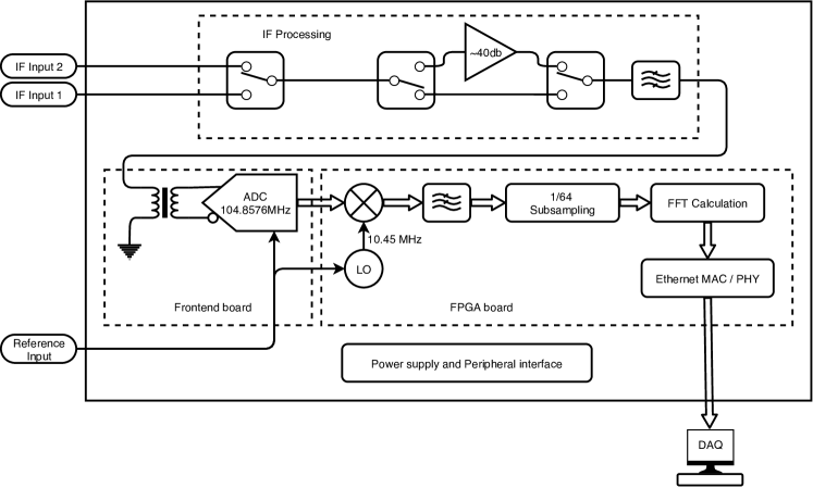
The fabricated FPGA DAQ system is shown in Fig. 3. The system is divided into three sections of (1) Power supply and peripheral interface, (2) IF processing path, and (3) frontend and FPGA board. The power supply and peripheral interface part includes a linear power supply unit followed by a few voltage regulators, plus several logic translators to drive external components. The IF processing path, the frontend and FPGA board are described in the following subsections.

II.2 IF processing path design
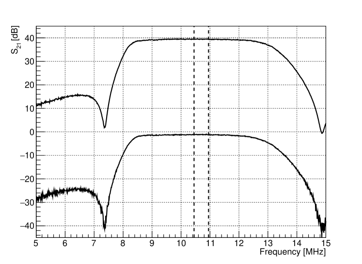
While the FPGA DAQ system can perform FFT on the signals from a single channel, it can accept two different sources of input, such as an input for a calibration signal. An RF switch (Mini-CircuitsZSW2-63DR+, insertion loss 0.33 dB at 10.7 MHz) selects the input source. Two of the same switch components are used to select (by-) passing the RF amplifier, for additional signal amplification. The gain, noise level, and frequency range of the amplifier (Mini-CircuitsZKL-1R5+) are 40 dB (typical), 3 dB (typical), and 10 - 1500 MHz, respectively. The last stage of the IF processing path is equipped with a band-pass filter (Mini-CircuitsSBP-10.7+) with a 1.5 dB pass band of 9.5 - 11.5 MHz with 0.86 dB insertion loss at 10.7 MHz, in order to suppress the out-band noise. Figure 4 shows the transmission performance of the IF processing path for both cases, of using amplifier or not. In the analysis window, the gains (or losses) of the IF processing path are 39.5 dB or -1.16 dB when using an amplifier or by-passing it, respectively.
II.3 ADC and Frontend board
The frontend board is composed of an ADC chip, impedance matching network, clock manipulator, and ADC peripheral control circuit.
The employed ADC is a Texas InstrumentADS4149 ref:WEB_ADS4149 with 14 bit 250 MS/s, and 2 V dynamic range. It is operated by an external reference clock at 104.8576 MHz, manipulated through a fast differential logic buffer. The sampling clock was chosen considering that the FFT algorithm can be optimized for samples ( is a positive integer). To achieve 100 Hz frequency width, time series data during is required. Also, from the Nyquist theorem, the sampling rate is supposed to be greater than , and over-sampling is a common practice to decrease the ADC quantization noise. Therefore, a sampling rate above 100 MHz was requested, resulting in a sampling rate. The sampling clock signal is supplied from external equipment to get the benefit of a high performance signal generator synchronized with a standard clock reference.
Because it is not necessary to change the ADC parameters during operation, external ADC control lines are all removed to avoid digital noise from the control signals feeding into the RF signal. The frontend board is connected to the FPGA board through a 400-pin LPC-FMC (FPGA Mezzanine Card) connector.
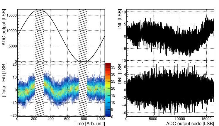
Figure 5 shows the key performances of the ADC, tested with a sinusoidal wave signal. The amplitude of the test signal was set slightly bigger than the dynamic range of the ADC, in order to avoid any effect near the edge of the dynamic range, or distortion of the signal near the local maximum and minimum. This results truncate the observed ADC data, as shown in the left-top plot in Fig. 5. A fit of the data to a truncated sinusoidal function was performed to estimate the input signal, where the fit residual of data in 160 cycles is shown in the left-bottom plot. The Integral Non-Linearity (INL) defined by the deviation of the observed ADC code from the expected ADC code (from fit), and the Differential Non-Linearity (DNL) defined by the deviation of the observed ADC codes of a bin to the adjacent bin, are shown in the right plot. The fit deviation, INL, and DNL are all a few LSB (Least Significant Bit) level, which is significantly smaller than the ADC dynamic range (14 bits).
II.4 FPGA board
For design simplicity, a commercial FPGA evaluation board, XilinxKCU105 ref:WEB_KCU105 was used. This board features the Xilinx UltrascaleXCKU040-2FFVA1156E FPGA. The FPGA and the evaluation board were chosen considering the foreseen logic cell requirement of the future logic upgrade of, for example, multiple analog channel processing. The board connects the frontend board to receive digitized IF signals, and several peripheral components for control and monitoring are connected through General Purpose Input and Output (GPIO) connectors.
III Design of the FPGA firmware
The FFT of samples is not practically possible with FPGA because of limited logic resources. However, the width of the signal window is only 500 kHz, therefore “Zoomed-FFT” techniques can be applied: the time series data is digitally down-converted to baseband. After applying the digital filter, the signal is again sub-sampled for every samples, as the required frequency width is only 100 Hz. The FFT is applied to the sub-sampled data, resulting FFT data. The lower 5001 points data are sent to the DAQ as a result.
A block diagram of the FPGA firmware is shown in Fig. 6. The core components for the FFT process are explained in the following subsections. Those components are operating with the ADC clock at 104.8576 MHz, while the Gigabit Transceiver (GT) operates with a GT reference clock at 125 MHz, which is provided by an on-board jitter cleaner IC. The “Internal Sync Signal” is generated by counting the ADC clock up to , which is used to synchronize all the FFT processing components. The system configuration is done by an Ethernet communication with a DAQ computer, which is described in Section III.4. A processor core for the system interface and monitor is designed by using MicroBlaze Soft Processor Core IP ref:ublaze of VivadoDesign Suite ref:vivado . The overall utilization of the FPGA resources of the firmware is around 5.4 %.
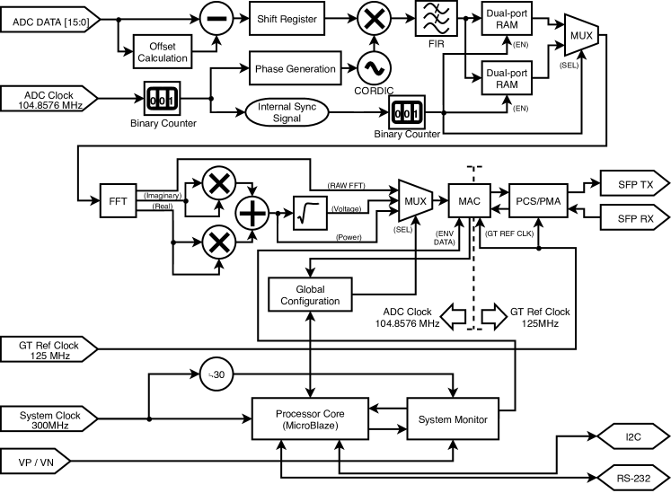
III.1 Digital mixing for down-conversion
The signal mixing means multiplying the RF signal with a reference sinusoidal signal (the LO signal), in order to convert the frequency range of the signal. From the Fourier transform, any signal can be written as , where represents the amplitude of the signal component with respect to angular velocity . Assuming a sinusoidal wave , then,
| (2) |
This implies that, by multiplying the sinusoidal reference signal to any signal, the frequency divides into two bands, at and . By selecting only the upper or lower part, the signal can be up- or down- converted, respectively, without losing the information in the signal.
The axion signal is also down-converted from an RF signal to an IF band, during the signal processing network before reaching the DAQ equipment. In the FPGA DAQ, it is subsequently down-converted from the IF band to the baseband by using a digital multiplication algorithm (i.e., not using a hardware mixer component). It should be noted that direct down-conversion to the baseband before reaching the ADC is not preferred, due to the existence of 1/f noise which may degrades the axion signal. Also the wide-band mixer component selection is limited on the market, which forces to employ multiple RF mixer components that possibly degrades the axion signal. Since the IF is fixed to 10.7 MHz and the analysis window is 500 kHz, the LO frequency of digital mixing is determined to be , so that the lower limit of the analysis window corresponds to DC after the down-conversion. The LO signal is generated by using CORDIC LogiCORE IP ref:cordic of VivadoDesign Suite.
III.2 Low pass filter
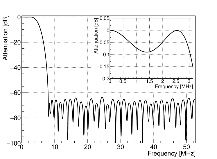
Since the IF signal will be mixed to two side band signals, corresponding to the sum and difference of the IF and LO frequencies, the low pass filter is equipped to select the lower-band signal only. The Finite Impulse Response (FIR) filter is designed using the Parks-McClellan optimal FIR filter design ref:octavefir of GNU Octave program ref:octave , while it is implemented in the FPGA logic using the FIR Compiler LogiCORE IP ref:fir of VivadoDesign Suite. The analysis window after down-conversion corresponds to DC - 500 kHz, and the high-side image signal is located around 21.15 MHz, therefore, the passband of FIR filter is designed up to 3 MHz with an attenuation ripple less than 0.1 dB. The stopband of the FIR is defined from 8 MHz, with attenuation of at least -60 dB. The calculated frequency response is shown in Fig. 7.
III.3 Sub-sampling and FFT
The maximum frequency of the baseband signal is 500 kHz. For efficient subsampling of samples while maintaining a frequency width of 100 Hz, the subsampling rate of is applied, resulting in a 1/64 subsampling to 16384 () samples out of samples. This subsampling rate is more than two times that of the analysis window (500 kHz), satisfying the Nyquist theorem. To achieve real-time and pipelined processing, dual block RAMs were constructed in the FPGA logic, in order to record next 16384 samples while transacting the previous 16384 samples to the FFT logic.
The FFT process was designed using the Fast Fourier Transform LogiCORE IP ref:fft of VivadoDesign Suite. It calculates 16384 points of FFT data, but only the lower 5001 points are selected (up to 500 kHz) and sent to the DAQ. The architecture of the FFT is the Radix-2 Decimation In Frequency (DIF) method (“Pipelined Streaming IO”). The FFT calculates the real and imaginary parts simultaneously, to yield signal power in a linear scale in an arbitrary unit.
III.4 Ethernet protocol design
To enable real-time data transaction to the DAQ, a special Ethernet protocol was designed in the FPGA logic. The data rate of the FFT can be calculated as follows. The size of a point in the FFT result is 8 bytes, and 5001 data points are calculated during 10 msec. Then, ignoring the transaction overhead, the averaged data rate is at least or 32 Mbps. In order to provide sufficient transaction bandwidth, 1 GbE Ethernet was employed to connect the system to the DAQ. The merit of using 1 GbE is that interface hardware and software with very high reliability are commonly available, from which the system design becomes significantly simpler. Also, it allows any future design upgrades with higher data rates.
For simplicity in design, one-to-one direct connection between the FPGA DAQ system and DAQ computer without any network routing device in between is assumed. The protocol or packet structure for FPGA DAQ is designed based on a custom, non-standard Ethernet (in the data link layer (layer-2) of the OSI model ref:osimodel ) packet design. The entire packet structure is shown in Fig. 8. The fields related to the FPGA DAQ are explained below. Other fields are defined in IEEE 802.3 ref:ieee802 .
- EVTID
-
This indicates the event number of the FPGA DAQ data, which is supposed to increase by one at the start of the new sampling every 10 msec.
- PKTID
-
Since one event’s data is split into several Ethernet packets, this field indicates the packet number inside the same event. 32 packets are required to send 5001 FFT data point.
- TIMESTAMP
-
This 32 bits-long field contains the clock data for the time of packet being sent, with resolution. The field value is used to check whether the packets are being sent in real-time or any transaction error has occurred. This field completes the FPGA DAQ data header.
- SAMPLE DATA
-
This 160-times recurring field contains FFT data. Every Ethernet packet sends 160 samples, therefore, 1280 bytes in total.
- IDENTIFIER
-
This field value is fixed to 0x4341505000 (“CAPP\0”) in order to identify the end of the data stream.
- MODE
-
This field contains the DAQ mode information.
- NSAMPLE
-
The number of FPGA DAQ data points in this packet. If every transaction is alright, this value should be 160 for all samples up to the 31-th packet, and 41 for the last (32nd) packet. This field completes the FPGA DAQ data trailer, and also completes the Ethernet payload.
A Media Access Controller (MAC) is customary designed for handling this packet structure and converting it into Gigabit Media Independent Interface (GMII). The Physical Coding Sublayer (PCS) and Physical Medium Attachment (PMA) receive the GMII data and send it to the DAQ computer through the 1 GbE link. The PCS/PMA was designed using 1G/2.5G Ethernet PCS/PMA or SGMII LogiCORE IP ref:pcspma of the VivadoDesign Suite.
| Byte | 1 | 2 | 3 | 4 | 5 | 6 | 7 | 8 |
|---|---|---|---|---|---|---|---|---|
| PREAMBLE | SFD | |||||||
| Ethernet header | DESTMAC | SRCMAC | ||||||
| SRCMAC | TYPE | |||||||
| FPGA DAQ header | EVTID | PKTID | TIMESTAMP | |||||
| SAMPLE DATA #1 | ||||||||
| FPGA DAQ data | ||||||||
| SAMPLE DATA #160 | ||||||||
| FPGA DAQ trailer | IDENTIFIER | MODE | NSAMPLE | |||||
| Ethernet trailer | FCS | |||||||
IV Performance of the FPGA DAQ system
The first conceptual design of the FPGA DAQ was prepared in IBS/CAPP and fabricated by an external company along with the FPGA logic design in 2018. The design was revised in 2019 to improve the IF processing path and frontend circuit to reach a better noise level. The revised products were fabricated and tested in IBS/CAPP during 2020 and deployed in one of the CULTASK experiment for further tests in a real experimental environment. The test results on the noise level, linearity of signal measurement, and DAQ efficiency are described below.
IV.1 Noise level
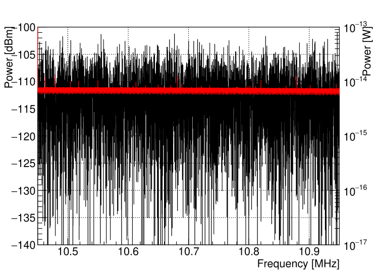
Figure 9 shows the power spectrum with a 50 terminated input, corresponding to the effective noise level of the FPGA DAQ system, after applying the calibration result discussed in Section IV.3. The noise level of a single measurement (the black trace in Fig. 9) fluctuates along the frequency, ranging from around -150 dBm to -100 dBm. Because the noise voltage is Gaussian-distributed, and the power of each spectrum bin follows distribution of degree 2, averaging the number of measurements in a spectrum bin reduces the fluctuation in the measurement, following the radiometer equation, as discussed in detail in Section IV.5. The red trace in Fig. 9 shows the average of 100,000 times measurements, clearly showing the reduction in noise fluctuation. The averaged noise level of 100,000 times measurements is -111.7 dBm, and the effective noise floor defined by the maximum of the noise distribution is -108.8 dBm. The first spectrum bin somehow shows an incorrect measurement almost every time, which can be ignored in the real measurement. It also shows clear evidences of spurious peaks which might come from the signal mixing or an external noise intrusion, which, however, does not affect the axion experimental measurement of which the noise level after amplification through the RF receiver chain is much higher than the spurious peaks.
IV.2 Frequency reconstruction and gain stability along frequency
Correct reconstruction of the measurement frequency is very important in the axion experiment, as the frequency represents the axion mass. While the measurement frequency is controlled by the tuning system of the cavity resonant frequency and the RF signal down-conversion to IF before reaching to the FPGA DAQ, the FPGA DAQ have to measure the frequency correctly without any distortion. In order to confirm this, the dependence of the measured frequency bin number (defined as ) to the input frequency, and the existence of missing , were examined. The input signal was sinusoidal signal with the frequency ranging from 10.45 MHz to 10.95 MHz with 100 Hz step, and the peak position (representing ) and its height of FFT (i.e., measured power of input signal before applying calibration) were measured. The ranges from 0 to 5000, supposedly corresponding to 10.45 MHz and 10.95 MHz. The input signal frequency was converted to the expected input frequency bin number, , by
| (3) |
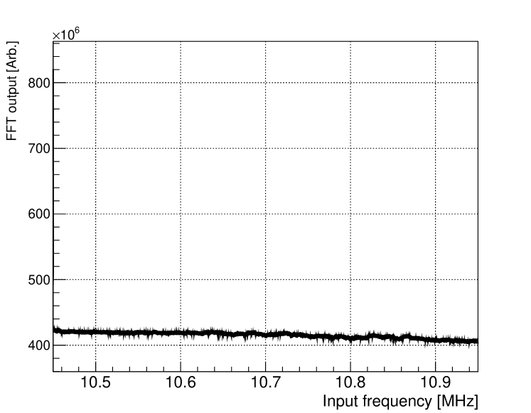
Over the entire frequency range from 10.45 MHz to 10.95 MHz, the differences between and were zero, meaning that the signal frequency can be calculated using Eq. 3 without any discrepancy. All were evenly distributed over the entire frequency range without any missing value in the measurement window. The measured power distribution over the entire frequency range is shown in Fig. 10. A notable gain drop of a maximum 0.1 dB was observed when the frequency was increasing, partly due to the variation in gain of the low pass filter, as shown in Fig. 7. The measured power of the first frequency bin (corresponding 10.45 MHz) was always comparably different than the flat gain distribution, which is not understood yet. This does not affect the real experiment, since the corresponding frequency data can be discarded every time as it is away from the cavity resonant frequency. This discarding will result in reducing the measured frequency range 100 Hz only.
IV.3 Linearity of power measurement and power calibration
While the frequency measurement is exact in the FFT output, the power measurement requires calibration using an external reference source. The calibration procedure uses a signal generator for the calibrated power, and the FFT output codes are measured while varying power. Several different frequency points are measured to understand the frequency dependence. The data with the correct signal frequency recovery (the filled points in the upper plot in Fig. 11) are used for 5th-order polynomial function fit to obtain the calibration model. From the relative deviation of the model, shown in the lower plot of Fig. 11, the uncertainty from the calibration was estimated to be less than 0.5 %, in the worst case of near-noise floor measurement. A clear evidence of the dependence to the frequency was observed, for example, the relative deviation were always positive for 10.5 MHz data, while always negative for 10.8999 MHz data. This is partly because of the gain change along the frequency as described in the Section IV.2. The relative deviation also shows a fluctuation between the nearby frequency bins, of which the reason is not understood yet. However, all these dependence are less than the overall calibration uncertainty of 0.5 %. The calibration dependence on the temperatures of various parts of the FPGA DAQ and the bias voltages were checked, however, no significant dependence was observed in an one-day continuous DAQ data. A long term stability is still being checked with a CULTASK experiment setup.

IV.4 DAQ efficiency
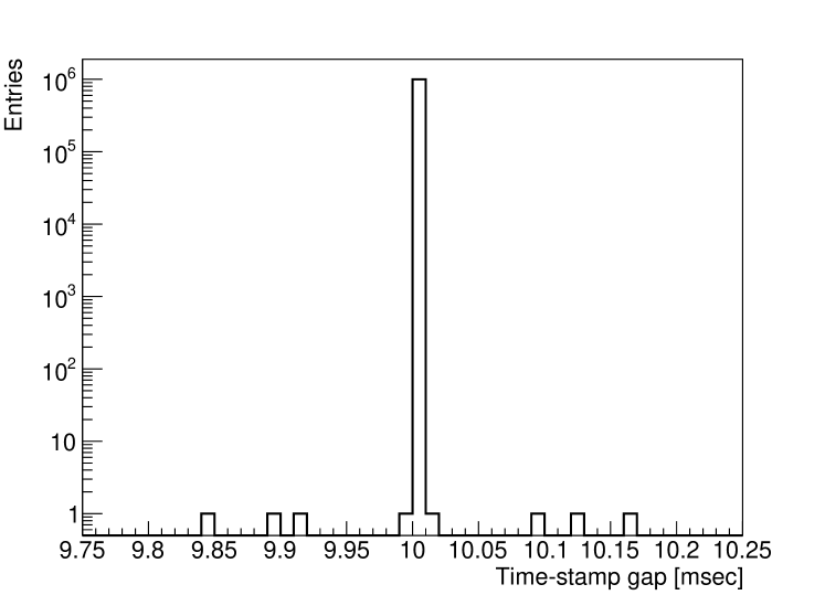
The DAQ efficiency was estimated by using the time-stamp data of the data packet. Every Ethernet packet contains time-stamp data indicating the -resolution wall time when the packet is sent to the DAQ computer. Figure 12 shows the distribution in time-stamp differences between adjacent events, for events from 2.8 hours continuous DAQ. The network interface card effectively filters out any events with an incorrect Frame Check Sequence (FCS), and the event number recorded in this data sample increased by one for all events, which means no data loss occurred during the Ethernet transmission. The observed time-stamp difference between adjacent events was in average, without any overflowing or underflowing events. This means all the FFT data during this measurement time was completely transferred and recorded in the DAQ.
It should be noted that this 100 % DAQ efficiency could be achieved not only owing to the special design on the pipelined signal processing and the Ethernet packet and protocol of the FPGA DAQ, but also due to the idle status of the DAQ computer. The Network Interface Card and its driver software of the DAQ computer may not contain enough buffer memory in order not to discard any data that was not read by the operating system. Therefore, in order not to lose any data transmitted from the FPGA DAQ, the DAQ computer is expected to remain idle status. This requires a dedicated DAQ computer for the FPGA DAQ, not shared by any other part of DAQ.
IV.5 Axion signal detection analysis with pseudo-data
Assuming the system temperature of the cryogenic system of axion experiment is 1 K, the noise power is where is the Boltzmann constant, is the system temperature, and is frequency resolution. The postulated axion signal power is around , which is lower than the noise level. The Signal-to-Noise Ratio (SNR) of the axion detection can be improved by increasing the number of measurements ref:admx ; ref:haystac , as depicted in the Radiometer equation:
| (4) |
where is the axion signal power of equivalent temperature , and is the number of measurements during the measurement time . As a demonstration of the axion signal detection principle using the Radiometer equation, in this pseudo-data test, a combined signal of arbitrary white noise and a sinusoidal signal of a known frequency and various power levels were supplied to the FPGA DAQ system, to understand the SNR improvement over the repeated measurement.
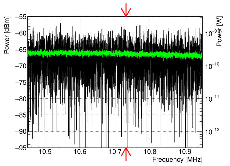
The measured noise level of the CULTASK experiment is around dBm after passing through several cryogenic and room-temperature amplifiers. The white noise supplied to the FPGA DAQ system was set to around -66.3 dBm, and generated by an arbitrary function generator. Another RF signal generator was used to generate 10.73141592 MHz signal which was combined with the white noise through an RF combiner component. Figure 13 compares the measured spectrum of a single measurement (black) and 100 times average (green), when the input signal power is -83.8 dBm combined with -66.3 dBm white noise. In this measurement, the signal is not observed.
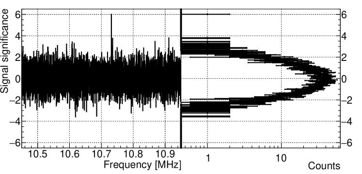
The pseudo-axion experimental spectrum was measured 100,000 times and averaged. In order to determine the power excess, the averaged spectrum was divided by the baseline estimation from the Savitzky-Golay filter, and one is subtracted ref:haystac . The standard normal deviation of the power excess histogram, regarded as the signal significance or the SNR, is shown in Fig. 14. In this figure, the signal power was -83.8 dBm, while the average number was 100,000. The signal at 10.7314 MHz was clearly observed with deviation. Note that the SNR estimated from the radiometer equation was 5.6, which is comparable with this measurement.
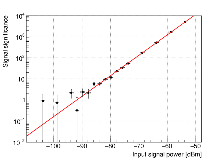
Assuming the deviation represents the possible existence of an axion signal candidate, the input signal power was scanned from near -50 dBm to -100 dBm, with 100,000 times average for each scan. The signal significance was calculated for each power scan, and the result is shown in Fig. 15. From an exponential function fit, it was estimated that a -87.0 dBm signal will result in a signal significance under -66.3 dBm white noise, when 100,000 spectra are averaged. In a real experiment, frequency points of more than significance is regarded as an axion signal candidate frequency, which is subject to a re-scanning experiment for further SNR improvement.
V Summary and conclusion
An FPGA based real-time DAQ system was constructed and tested for the CULTASK axion experiment. The FPGA DAQ system is optimally designed for RF spectrum measurement in the axion experiment, especially with regard to DAQ efficiency. The 100,000 times averaged noise level of the FPGA DAQ system was around -111.7 dBm which meets the requirement. It was confirmed that the repeated measurement would increase the SNR, following the radiometer equation. In case of 100,000 times measurement, under -68.3 dBm noise level, the axion signal of -87.0 dBm can be detected with significance. Several FPGA DAQ systems are constructed in IBS/CAPP and will be used as the main DAQ equipment of the CULTASK experiment.
Acknowledgments
This work was supported by the Institute for Basic Science (IBS-R017-D1-2021-a00) of Korea. The author M. J. Lee would like to thank Mr. Byung-gyu Kim and others of Ubicom technology, Korea, for their help on constructing the first version of the FPGA DAQ system.
References
- (1) R. D. Peccei and H, R, Quinn, CP Conservation in the Presence of Pseudoparticles, Physical Review Letters 38 (1977) 1440.
- (2) S. Weinberg, A New Light Boson?, Physical Review Letters 40 (1978) 223.
- (3) F. Wilczek, Problem of Strong P and T Invariance in the Presence of Instantons, Physical Review Letters 40 (1978) 279.
- (4) Jihn E. Kim, Weak-Interaction Singlet and Strong CP Invariance, Physical Review Letters 43 (1979) 103.
- (5) S. Lee et al., Axion Dark Matter Search around 6.7 eV, Physical Review Letters 124 (2020) 101802.
- (6) S. Ahn et al., Improved axion haloscope search analysis, Journal of High Energy Physics 2021 (2021) 297.
- (7) O. Kwon et al., First Results from an Axion Haloscope at CAPP around 10.7 eV, Physical Review Letters 126 (2021) 191802.
- (8) P. Sikivie, Detection rates for “invisible”-axion searches, Physical Review D 32 (1985) 2988.
- (9) H. Peng et al., Cryogenic cavity detector for a large-scale cold dark-matter axion search, Nuclear Instruments and Methods in Physics A 444 (2000) 569.
- (10) ADS4149 14-Bit, 250-MSPS Analog-to-Digital Converter (ADC), http://www.ti.com/product/ads4149, 2021.
- (11) Xilinx Kintex UltraScale FPGA KCU105 Evaluation Kit, https://www.xilinx.com/products/boards-and-kits/kcu105.html, 2021.
- (12) MicroBlaze Soft Processor Core, https://www.xilinx.com/products/design-tools/microblaze.html, 2021.
- (13) Vivado, https://www.xilinx.com/support/university/vivado.html, 2021.
- (14) CORDIC, https://www.xilinx.com/products/intellectual-property/cordic.html, 2021.
- (15) L. R. Rabiner, J. H. McClellan and T. W. Parks, FIR Digital Filter Design Techniques Using Weighted Chebyshev Approximations, Proceedings of the IEEE 63 (1975) 595.
- (16) GNU Octave, https://www.gnu.org/software/octave, 2021.
- (17) FIR Compiler, https://www.xilinx.com/products/intellectual-property/fir_compiler.html, 2021.
- (18) Fast Fourier Transform (FFT), https://www.xilinx.com/products/intellectual-property/fft.html, 2021.
- (19) Information technology — Open Systems Interconnection — Basic Reference Model: The Basic Model, International Standard ISO/IEC 7498-1:1994.
- (20) IEEE Standard for Ethernet, IEEE Standard (2012) 802.3-2012.
- (21) Ethernet 1G/2.5G BASE-X PCS/PMA or SGMII, https://www.xilinx.com/products/intellectual-property/do-di-gmiito1gbsxpcs.html, 2021.
- (22) B. M. Brubaker et al., HAYSTAC axion search analysis procedure, Physical Review D 96 (2017) 123008.