Surface step states and Majorana end states in profiled topological insulator thin films
Abstract
The protected helical surface states in thin films of topological insulators (TI) are subject to inter-surface hybridisation. This leads to gap opening and spin texture changes as witnessed in photoemission and quasiparticle interference investigations. Theoretical studies show that universally the hybridisation energy exhibits exponential decay as well as sign oscillations as function of film thickness, depending on the effective band parameters of the material. When a step is introduced in the TI film e.g. by profiling the substrate such that the hybridisation has different signs on both sides of the step, 1D bound states appear within the hybridisation gap which decay exponentially with distance from the step. The step bound states have linear dispersion and inherit the helical spin locking from the surface states and are therefore non-degenerate. When the substrate becomes an s-wave superconductor Majorana zero modes located at the step ends are created inside the superconducting gap. The proposed scenario involves just a suitably stepped interface of superconductor and TI and therefore may be a most simple device being able to host Majorana zero modes.
I Introduction
The surfaces of strong topological insulators (TI) like Bi2Se3, Bi2Te3 and Sb2Te3 carry spin-locked non-degenerate helical surface
states. As long as the surfaces are isolated, i.e. their distance is much larger than the surface state decay length
into the bulk the 2D dispersion is described by isotropic Dirac cones to lowest order in momentum counted from
the time-reversal invariant (TRI) points and by warped cones with sixfold symmetry due to higher order terms. They have been verified
indirectly by magnetotransport measurements Taskin and Ando (2011); Taskin et al. (2012) as well as directly
by photoemission Hsieh et al. (2009); Chen et al. (2009); Kuroda et al. (2010); Hoefer et al. (2014) and surface tunneling Roushan et al. (2009); Zhang et al. (2009); Alpichshev et al. (2010); Okada et al. (2011); Cheng et al. (2012); Kohsaka et al. (2017); Lee et al. (2009) experiments, the latter were explained in numerous
theoretical investigations Lee et al. (2009); Zhou et al. (2009); Rüßmann et al. (2021).
This simple situation changes in an interesting manner when one considers TI thin films with thickness small enough so that
inter-surface hybridisation of bottom (B) and top (T) surface states occurs. Due to the interaction topological protection for
states close to the Dirac point is lifted and a hybridisation gap in the excitation spectrum opens. This has indeed been verified directly by photoemission Zhang et al. (2010); Neupane et al. (2014) but also by a sudden breakdown of weak anti-localisation in magnetotransport Taskin and Ando (2011); Taskin et al. (2012) as function of film thickness when the latter falls below about five quintuple layers (QL). The effective hybridisation between the surface states has been calculated Lu et al. (2010); Asmar et al. (2018, 2021) solving the thin film boundary value problem for an effective Hamiltonian of the bulk. Due to the constrained film geometry
the effective inter-surface hybridisation not only decreases exponentially with film thickness but also generally oscillates
as function of thickness d with an oscillation period depending on the material parameters. This should be again visible in the photoemission gap and in the concommitant oscillation of quasiparticle interference (QPI) patterns predicted in Ref. Thalmeier and Akbari, 2020.
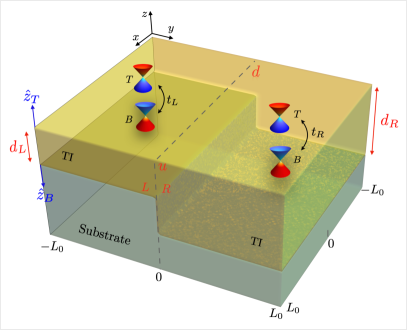
Aside from the modulated excitation gap at the Dirac point the oscillation of gives rise to another novel and highly interesting scenario which is the subject of this investigation. Suppose the film thickness is not constant but changes in a steplike manner at a certain lateral position (see Fig. 1). If the thickness to the left and right of the step is chosen in such a way that the hybridisation and have opposite signs on the two sides of the step then a helical non-degenerate bound state within the hybridisation gap may appear which is spatially located at the step and has a linear dispersion. If found experimentally this would entail a further interesting speculative possibility: Once the substrate of the step-profiled TI becomes a simple s-wave spin singlet superconductor the proximity effect will open a superconducting gap in the dispersion of nondegenerate (spin-locked) step state. This is a typical situation that can create Majorana end states. Such scenario have previously investigated e.g. with TI nanowires on SC substrate Sau and Tewari (2021); Sau et al. (2010); Stanescu and Tewari (2013); Cook and Franz (2011); Cook et al. (2012); Das et al. (2012) which may need the application of a magnetic flux through the wire. In alternative devices the wire has to be itself ferromagnetic Livanas et al. (2019) or heterostructures with ferromagnetic layers are used Stanescu and Tewari (2013). In the present scenario no magnetic field has to be applied, a properly chosen step of the TI profile on the substrate is sufficient to create the possibility for Majorana states at the step ends. This seems to be a most simple way to realise these states in a realistic geometry.
II Isotropic Dirac surface state model for TI
As a starting point for the homogeneous thin film we use the isotropic TI surface state model on the top (T) and bottom (B) surface of the film. We will use indices and associated Pauli matrix vectors to denote two dimensional T/B surface, spin and helicity spaces. The unit in each space is denoted by . On a single isolated surface, using the operator basis , the isotropic 2D model Hamiltonian is given by
| (1) |
where is the wave vector counted from the TRI Dirac point, the spin, the surface normal and the velocity, furthermore and . This expression is proportional to the helicity operator , namely . The eigenvalues or dispersions of the Dirac cone and associated eigenvectors in the spin basis are described by
| (4) |
where the columns of the unitary matrix are the helical eigenstates . In this basis the helicity operator is simply represented by the Pauli matrix . Furthermore is the azimuthal angle of the k-vector.
III Hybridisation and gap opening of surface states in TI thin films
In a TI film with thickness much larger than the surface state decay length the top and bottom surfaces may be considered as independent surface states. One only has to keep in mind that surface normals are oppositely oriented to the global direction, i.e. . Therefore helicities for both energies are also opposite on T, B surfaces according to and therefore . However, when the film thickness is reduced (below a few quintuple layers) the T,B surface states overlap and a hybridisation of equal spin (and therefore equal helicity) eigenstates develops. This problem has been fundamentally treated and analyzed in great generality in the work of Asmar et al Asmar et al. (2018) and also in Ref. Shan et al., 2010. Here we use a simplified model with a k-independent effective hybridisation element that depends, however, on film thickness . The thin film surface states Hamiltonian is then given in spin representation Thalmeier and Akbari (2020) using ,
| (5) | ||||
or in helicity representation according to
| (6) |
The eigenvalues of the film Hamiltonian are then obtained as
| (7) |
Which exhibit a thickness dependent hybridisation gap at the Dirac point . Each of these dispersion branches is twofold degenerate which is inherited from the (T,B) degeneracy of states in the uncoupled case. The degeneracy is lifted if the bottom surface experiences an effective bias due to the substrate effect. This can be described by adding a term to Eq. (5). Then the split hybridised surface bands are given by
| (8) |
where split band indices refer to inside the square root. Since the above substrate term can in principle be canceled by an applied bias voltage term at the substrate we will keep the degenerate thin film model of Eq. (7). Furthermore the chemical potential can be controlled by applying a gate voltage at the TI surface.
III.1 The oscillation model of hybridisation with film thickness
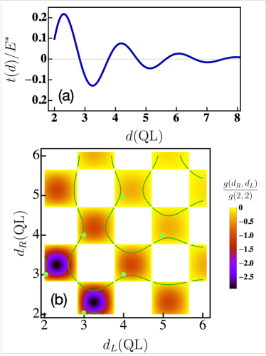
The thickness dependent effective hybridisation may be obtained from the solution of a subtle boundary value problem for the thin film Asmar et al. (2018), starting form the Hamiltonian of the bulk bands. It may be represented by the phenomenological form Asmar et al. (2018); Thalmeier and Akbari (2020)
| (9) |
Here the energy and thickness scales are determined by the parameters of bulk bands Asmar et al. (2018); Thalmeier and Akbari (2020). As an example we give the theoretical values for Bi2Te3 in terms of natural units meV and Å, respectively as . As expected the expression contains an exponential decay with increasing thickness but, in order to satisfy boundary conditions, also an oscillatory term, whose physical origin was derived in Ref. Asmar et al. (2018). The hybridisation is obtained as a perturbation integral of an effective inter-surface tunneling Hamiltonian connecting the uncoupled surface state wave functions. The decay length of the latter perpendicular to the surface may become a complex number, depending on the bulk band parameters. This leads to oscillating decay of the wave function which is inherited by the hybridisation integral. We note that the vanishing t(d) for thin films at the nodes (Fig. 2) does not mean the surface states should be considered as decoupled as for large d in the bulk case but they rather indicate the destructive interference of both surface wave function in the hybridisation integral. These thickness oscillations of play an essential role in the present investigation and its consequences have before been studied in view of its influence on quasiparticle interference (QPI) patterns Thalmeier and Akbari (2020). According to the theoretical estimation of parameters Asmar et al. (2018, 2021) the oscillations of the gap should be pronounced in Bi2Te3 and Sb2Te3 but not in Bi2Se3. In the latter only half an oscillation period appears which is strongly damped by the rapid exponentioal decay of . The observable quantity is the (rectified) oscillation of inter-surface hybridisation gap . Since it can reasonably only be compared for films with identical surface terminations one is restricted to a discrete set of values for with integer multiples of quintuple layers. Therefore weak oscillations of may not easily be identified. The hybridisation gap opening as function of film thickness with integer number of QL has been investigated by ARPES Zhang et al. (2010) for Bi2Se3. The predicted exponential decay of with increasing film thickness was observed but no clear evidence for the half oscillation period was found. It was argued Thalmeier and Akbari (2020) that a modest change of the theoretical bulk band parameters leading to different values of in Eq. (9) could account for the suppression of the half oscillation. In fact charge transfer and bulk band bending effects due to the substrate have not been included in the theoretical model employed here but may influence the surface state energies Zhang et al. (2010) and possibly the above oscillation parameters. However, the origin of hybridisation gap oscillation is of universal nature enforced by boundary conditions due to the constrained geometry of thin films Asmar et al. (2018) and therefore it may appear whenever the bulk band parameters of the 3D TI lead to suitable scales with , i.e. a considerable number of oscillations before decays. Therefore they should appear in TI material with more favourable scale parameters such as is prediced for Bi2Te3 or Sb2Te3 (Fig. 2a). Sofar no systematic film thickness variation of the hybridsation gap in these materials has been investigated with either ARPES or QPI methods.
Due to their universal origin we are confident that the gap oscillations will eventually be found in thin films of a suitable TI material. This expectation is the starting point for the following investigation of intriguing appearance of 1D topological states for profiled thin film geometry.
IV Creation of 1D step bound states inside the TI thin film gap
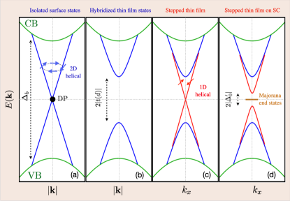
The TI surface state form linearly dispersing 2D bands or Dirac cones inside the bulk gap (Fig.3a) of the 3D TI material which is due to bulk spin-orbit coupling. For sufficiently thin films the Dirac cones themselves are opening a gap given by the size of the inter-surface hybridisation (Fig.3a). One might ask whether the creation of topologically protected in-gap states can be repeated by some means in a ‘Matrjoschka’-like fashion, creating 1D linearly dispersing bands within the hybridisation gap of 2D surface states. One way is to create domain walls of some sort on the surface with suitable properties. The easiest way to achieve a domain wall is by stepping the thin film (e.g. by stepping the substrate) so that the film thickness and hybridisation are different on both sides of the step (see illustration in Fig. 1). This possibility will be investigated in the following sections.
IV.1 Boundary and existence conditions and dispersion of bound states
Let us adopt a step geometry with the step extending along the -direction, separating the left (L) and right (R) regions of the surfaces at and the surface normals oriented parallel to (Fig. 1). Then, assuming a sharp step the -dependent inter-surface hybridisation is given by
| (10) |
where and , we assume is the sample length along (Fig. 1). At the moment we keep the relative size of arbitrary. To find out whether a localised state at the step develops one has to replace and in the Hamiltonian leading to the effective 1D problem (with parallel to the step treated as a fixed parameter) described in spin-surface space by
| (11) | ||||
If a localised bound state exists at the step it has to fulfil the envelope equation
| (12) |
with , i.e., lying inside the hybridisation gap of 2D surface states. It is convenient to introduce rescaled energies and which have the dimension of wave number or inverse length (units ). The wave function is a four spinor defined by ( for transposed):
| (13) |
For the the L,R sides of the step we use the following ansatz to solve Eq. (12) :
| (14) |
where and are given by the inverse decay lengths of the bound state localised at the step. Inserting into Eq. (12) we obtain
| (15) |
The second equation follows because the first one has to be fulfilled for both sides L and R simultaneously. The remaining relation to determine is obtained from the boundary condition at the step according to . These wave functions for step states with energies (Eq. (15)) are determined by the solutions of
| (24) |
The matrix has rank 2 and therefore 2 components and may be considered as free parameters for the solution. The other two components are obtained as
| (25) | ||||
The ratio is fixed by the continuity condition . From the two equations above we obtain
| (26) |
Taking the product and using the symmetrised Eq. (15) with , we finally arrive at the second relation
| (27) |
This equation together with the one in Eq. (15) may be solved by expressing them in terms of the (anti-) symmetrised quantities . After some algebra one obtains the simple relations
| (28) | ||||
For a localised step state within the thin film hybridisation gap one must have both . It is easy to see from the above expressions that this can only be possible if the we have the fundamental relation
| (29) |
where we defined . Inserting for these to cases into Eq. (15) for the step state energy we simply get, after reordering, the two linear dispersing energies:
| (30) |
which form two linear dispersing branches of 1D excitations localised at and moving along the step with an energy inside the thin-film hybridisation gaps for . We note that the dispersion relation, i.e. the velocity is independent of the size of hybridisations and hence of the asocciated asymmetric decay of the wave function perpendicular to the step. This non-degenerate step state as enforced by the boundary conditions exists as long as changes sign when crossing the step. It is therefore topologically protected as long as this condition is fulfilled. These 1D topological states inside the gap of hybridised 2D topological thin film states are schematically shown in Fig. 3(c). The velocity of 1D excitations (red) is asymptotically the same as those of the gapped and hybridized 2D surface excitations (blue).
IV.2 Eigenvectors and helicity of the step states
The four amplitudes of the wave function in Eq. (14) are obtained from Eqs. (25,26) and the condition that . They are the same on both sides L,R. For the two orthogonal states corresponding to , we obtain
| (39) |
The complete normalised wave functions of the two nondegenerate step states are finally given by
| (40) |
where the normalisation is with denoting half the step length in -direction and corresponding to the two possible cases of Eq. (29). Examples of the step wave functions for various integer QL thickness pairs are given in Fig. 4(a). These wave functions are eigenstates to the helicity operator. Since for the step states the latter is given by . The spinors (and also the total wave functions ) then fulfil . This property is inherited from the isolated T,B film states. Because of the 1D character of step states it means the spin is always locked perpendicular to , i.e. parallel to . It is also useful to consider the expectation values of the spin . One finds and . All other spin expectation values vanish. The eigenvectors define the field operators of helical step states according to (now using for 1D states):
| (41) | ||||
where the quasiparticle operator algebra for the 1D helical step states is defined by which is explicitly given by (using the abbreviation in Eq. (39));
| (42) | ||||
They fulfil the canonical anti-commutation relations . In terms of these 1D quasiparticle operators the 1D step state Hamiltonian may be written as (cf. Eq.(30))
| (43) |
These step states form the basis to construct Majorana end states through the proximity effect originating from the superconducting substrate. Before this, however we consider the situation for a more realistic step profile.
IV.3 Extension to bound states for soft steps
The existence of the 1D step states is not tied to having a sharp step. A more softer profile serves the same purpose, for example replacing Eq. (10) with a soft step of width :
To solve the wave equation Eq. (12) we now make a smooth envelope function ansatz instead of separating between L,R regime (Eq. (14)). It may be written as
| (45) |
with
| (46) | ||||
The form of spinors in Eq.(46) and the dispersions is the same as for the model with a sharp step. Here we defined the symmetrised expressions and . A comparison of step and envelope functions for various widths is presented in Fig. 4(b).
IV.4 Influence of the 2D warping term
Our investigation of step states is based on the underlying assumption that the influence of higher order warping terms for the 2D surface states can be neglected in the 1D step state formation. Firstly it is well known how to include them in the surface state formation of thin films where they modify the isotropic Dirac cones and circular Fermi surface into cones and Fermi surface with six-pronged ‘snowflake’ shape. A complete theory for homogeneous thin films, including the lowest order Dirac term (Eq. (1)), the warping term and the inter-surface hybridisation on the same footing has been developed in Ref. Thalmeier and Akbari (2020) leading to gapped and warped Dirac cones for the 2D thin film quasiparticles. The remaining question of importance here is how the warping will influence the formation of the 1D step states. We may understand this in a straightforward way by treating the warping as a perturbation (which vanishes for ). In the inhomogeneous film geometry the warping term in spin-surface presentation is given by
| (47) |
which has to be added to the unperturbed Hamiltonian in Eq. (11). Here is the warping parameter (for realistic values in TI see Ref. Thalmeier and Akbari (2020)). Then, using the 1D step wave functions of Eq. (40) the correction to the 1D step state dispersion Eq. (30) is given by
| (48) |
Writing the four component eigenvectors in Eq. (39) composed of obvious two-component parts we find that the expectation values and and therefore the warping correction to the 1D step state dispersion vanishes. We conclude that in first order in the warping scale the 1D step state Hamiltonian Eq. (43) is unchanged, therefore we can expect that the possible appearance of Majorana end states in the SC case as discussed in the next section is also unaffected by the warping term in this order for all momenta . Furthermore in the limit the warping perturbation effect vanishes intrinsically.
V Majorana zero modes in the SC proximity induced gap of 1D step states
In each of the two 1D bands of quasiparticles confined to the step the helical spin locking is protected since it is inherited from the 2D topological surface states. Therefore they may be considered as spin-locked 1D excitations. If they open a superconducting gap originating from the proximity effect of a superconducting substrate it is natural to expect Alicea (2012); Beenakker (2013); Elliott and Franz (2015); Sato and Fujimoto (2016); Chamon et al. (2010); Marra et al. (2021); Laubscher and Klinovaja (2021) the possible creation of Majorana zero modes (MZM) at the end of the step line which would lead to a zero-bias conductance peak in transport and tunneling experiments Das et al. (2012); Jeon et al. (2017); Aguado and Kouwenhoven (2020). Due to the locking of opposite spins in the helical state an underlying conventional singlet or s-wave superconductor with gap may be used instead of the difficult to realize p-wave superconductor necessary in spinless models Alicea (2012); Cook and Franz (2011); Laubscher and Klinovaja (2021). The topological state of a general 1D superconducting fermionic system is given by a topological invariant Kitaev (2001); Elliott and Franz (2015) where is the number of Fermi points including band degeneracy in one half of the BZ for the normal state. For the considered model (Eq. (30)) with one nondegenerate band we have and then characterizes a nontrivial topology of the superconducting state which may host Majorana zero modes as end states of the step. They are described by zero-energy solutions of Bogoliubov-deGennes (BdG) equations inside the SC gap and are characterised by quasiparticle operators which are identical to their conjugates. Previous scenarios to create Majorana states have mostly involved TI wires Cook and Franz (2011); Cook et al. (2012) on top of an s-wave SC and a flux passing through them to obtain the constituent 1D excitations from which Majorana states are formed. The present proposal is comparatively simple, it just takes the stepped interface between an s-wave SC and TI with the step playing the role of the flux penetrated wire.
V.1 Model for 1D BdG Hamiltonian of step states
Due to the proximity effects the spin-singlet pairs of the substrate can propagate a certain distance into the normal state of the TI which is governed by its coherence length of the latter de Gennes (1966). In the pure normal state it is given by which becomes large for low temperatures so that one may expect a still sizeable s-wave gap on the T,B surfaces of the topological insulator thin film. In order to formulate the effective BCS Hamiltonian for the 1D step states, however, we have to be aware that the proximity effect works on all 2D TI surface states. Therefore we first express the 1D Cooper pair operators formed from Eq. (42) by the 2D operator basis. We must keep in mind that the two 1D dispersions fulfill , therefore only inter-band pairing of states with opposite momenta and approximately equal energy are possible. For those pairs we have:
| (49) |
This means the inter-band pairing of spin-locked 1D quasiparticles naturally results from the proximity induced spin-singlet pairing of 2D surface states. Hereby we neglected on the right side i) triplet terms with equal amplitude since they cannot be induced by the s-wave substrate and ii) inter-(T,B) surface pairing of 2D helical states which is difficult to justify on the basis of the proximity effect. Then the pair amplitude is given by
| (50) | ||||
where are the s-wave order parameters on the two TI surfaces introduced by the proximity effect. If they may be almost equal. The proximity induced superconducting pair potential for the 1D surface states is then
| (51) | ||||
Introducing the Nambu spinors for the two 1D bands according to and adding the normal quasiparticle part in Eq. (43) we obtain for the total 1D step state BCS Hamiltonian
| (52) | ||||
Here the - and Pauli matrices act in the space of 1D bands and Nambu particle-hole space, respectively . For simplicity we first set i.e. the chemical potential lies at the Dirac point in Fig. 3, the case for general is treated at the end of this section. The explicit matrix form of is shown below. The step 1D quasiparticle energies in the superconducting state are then given by
| (53) |
where generally , i.e. the SC gap is inside the larger 2D hybridisation gap, except when is close to nodal points of (Fig. 2a).
V.2 MZM in-gap states at the step ends
Now we will search for zero energy solutions of the BdG Hamiltonian inside the SC gap and whose wave function has to be located within the step length , where is finite. Replacing in the above Hamiltonian we obtain the equation
| (54) |
In the space of four dimensional Nambu spinors the real space BdG Hamiltonian of Eq. (54) is represented as the matrix
| (55) |
Aside from a relative sign this matrix consists of two identical blocks due to the relation between inter-band pairings given in Eq. (49) and neglect of intra-band pairs. Using this matrix form which factorises into two blocks the BdG equation (Eq. (54)) may be solved by the ansatz of Eqs.(56,57) assuming , i.e. constant within the sample. The two solutions for each block decay exponentially either along or . This means they will be located at one of the ends of the step at or which we call (down) and (up), respectively (Fig.1). For the two blocks we arrive at the zero energy BdG wave functions
| (56) | ||||
where . The decay length of the end states is given by which may be written as which is proportional to the inverse BCS coherence length of the SC substrate. Here the first factor describes the gap reduction factor due to proximity effect and the second one the ratio of Fermi velocities in substrate and TI . Furthermore the amplitude vectors of the wave functions are
| (57) | ||||
The complete zero energy wave functions in the SC gap, including the -dependence from Eq. (40), is then given by
| (58) | |||||
where . The wave functions for blocks are related by permutation of the two 1D band states according to defined by the permutation operator which is a symmetry of the Hamiltonian. Therefore the wave functions of the zero energy states should also be symmetrized by taking the combination meaning
| (59) |
For these symmetrised zero energy wave functions we may construct their corresponding field operators according to
| (60) | ||||
where we used the real space representation . These operators satisfy the reality condition and and therefore represent two Majorana zero modes separated at the two ends of the step length. Their associated quasiparticle operators , corresponding to zero energy states with BdG wave functions in Eqs. (58,59) are then obtained as
| (61) | ||||
which fulfil the reality condition . These quasiparticle operators for the MZM satisfy the canonical Majorana anti-commutation rules and .
The real-space density profile
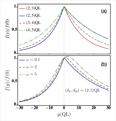
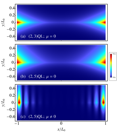
of these SC in-gap zero- energy states is governed by three (inverse) length scales: i) perpendicular to the step by and to the right and left and ii) parallel to the step by . This means that the Majorana density profile can be quite anisotropic and change rapidly as function of the relative
TI film thicknesses , on both sides of the step. In the general case when both and are not located close to the zeroes of the oscillatory function in Eq.(9) one has and therefore the Majorana profile is concentrated at the step with a more gradual decay along step direction (Fig. 5).
Finally we briefly give the results for the case of general position of the chemical potential inside the hybridization gap (Fig. 3(c)), cutting the 1D dispersions at finite wave vector once in the positive half of the BZ. In the SC state this leads to quasiparticle bands
| (62) |
which have now two branches emerging from and a SC gap , independent of the position of the chemical potential inside the hybridisation gap. The solutions for the MZM end states may be found in analogy to the above derivation. The essential difference lies in the MZM wave functions now given by
| (63) |
where and . Thus, in addition to the exponential decay from the ends there is an oscillation of MZM form factors which becomes faster than the decay for . Analogous to Eq. (60) the self-adjoint field operators of MZM modes can be written as
| (64) |
where we split into real and imaginary parts. we have now an additional Majorana pair complementing Eq. (61) and defined by the quasiparticle operators
| (65) | ||||
The doubling is related to the existence of two Bogoliubov excitation bands for arising from from points. Again the Majorana anti-commutation rules and are fulfilled, furthermore we have . The density profiles are and with similar as in Eq. (58). An example of the MZM profile for nonzero is shown in the bottom of Fig. 5 which exhibits the additional oscillatory behaviour.
VI Conclusion and outlook
In this work we have shown that the helical surface states in thin films of topological insulators may be manipulated in an interesting and promising way. It has previously been theoretically derived on general grounds that in thin films the surface states exhibit hybridisation due to inter-surface wave function overlap. This leads to a hybridisation energy that both decays exponentially and oscillates with film thickness depending on materials parameters and simultaneously leads to a gapping of the 2D helical surface states.
This can be exploited in a simple way by profiling the film thickness in a suitable manner, for example by introducing a step in film thickness via the substrate such that the inter-surface hybridisation has opposite sign on both sides of the step. This leads to the appearance of novel type of non-degenerate 1D helical states confined spatially to the step with linear dispersion and again helical spin locking. These states are protected by the sign change of the hybridisation and their decay perpendicular to the step is controlled by the modulus of the hybridisation energy. It should be possible to investigate the existence of these 1D step states and their dispersion by STM spectroscopy. Before this, however, it would be useful to check by STM and ARPES experiments whether homogeneous thin films indeed exhibit the theoretically predicted and prerequisite oscillations in hybridisation energy. This should immediately translate in the (rectified) oscillations of the gap size of coupled surface states. While Bi2Se3 does not seem to exhibit such oscillations the theoretical band parameters for Bi2Te3 and Sb2Te3 are apparently more favourable for their appearance.
If these conjectures can be experimentally verified in some cases another highly attractive possibility opens up: When the substrate becomes a simple s-wave superconductor the proximity effect leads to induced gapping of the 1D helical step states. Since the latter are nondegenerate fermions with spin locking this can create Majorana type zero-energy modes inside the proximity effect induced gap which are localised at the end of the steps where the gap drops to zero. Their inverse localisation lengths along and perpendicular to the step is proportional to the SC gap energy and left/right inter-surface hybridisation energies. These Majorana end states should, like 1D step states themselves be observable with STM spectroscopy. The present proposed scenario for creating Majorana states is exceedingly simple, requiring only a suitably profiled (s-wave superconducting substrate) to create the 1D step states. Since the latter are already nondegenerate by their helical spin-locked nature one should not need additional arrangements like applied magnetic fields or applying additional ferromagnetic layers which have been discussed before in the wire-type geometries for creating Majorana states.
The present simplistic geometry may be replaced by more elaborate ones. For example the step may not be extended to the whole width of the sample but may only be present for . When approaches the thicknesses may be gradually changed on both sides of the step to a common which satisfies . Then the 1D helical step state will also cease to exist at position within the thin film area. This would presumably simplify investigations by STM method and suppress unwanted effects from sample ends. Another extension would be a regular array of steps that are a certain distance apart leading to sign change of with period . This configuration would be suitable for studying the effects of 1D step state overlap. Finally one might form a ring-like step, i.e. a quantum dot with the proper thickness inside and outside the ring to support a 1D ring state. This should lead to a discretization of the linear dispersion of step states, depending on the diameter of the ring and the thickness variation characteristics. It is therefore certainly worthwhile to study these configurations and the possible in-gap (hybridisation, superconducting) states and their physical consequences further.
Acknowledgments
A. A. acknowledges the support of the Max Planck- POSTECH-Hsinchu Center for Complex Phase Materials, and financial support from the National Research Foundation (NRF) funded by the Ministry of Science of Korea (Grant No. 2016K1A4A01922028).
References
- Taskin and Ando (2011) A. A. Taskin and Y. Ando, Phys. Rev. B 84, 035301 (2011).
- Taskin et al. (2012) A. A. Taskin, S. Sasaki, K. Segawa, and Y. Ando, Phys. Rev. Lett. 109, 066803 (2012).
- Hsieh et al. (2009) D. Hsieh, Y. Xia, D. Qian, L. Wray, J. H. Dil, F. Meier, J. Osterwalder, L. Patthey, J. G. Checkelsky, N. P. Ong, A. V. Fedorov, H. Lin, A. Bansil, D. Grauer, Y. S. Hor, R. J. Cava, and M. Z. Hasan, Nature 460, 1101 (2009).
- Chen et al. (2009) Y. L. Chen, J. G. Analytis, J.-H. Chu, Z. K. Liu, S.-K. Mo, X. L. Qi, H. J. Zhang, D. H. Lu, X. Dai, Z. Fang, S. C. Zhang, I. R. Fisher, Z. Hussain, and Z.-X. Shen, Science 325, 178 (2009).
- Kuroda et al. (2010) K. Kuroda, M. Arita, K. Miyamoto, M. Ye, J. Jiang, A. Kimura, E. E. Krasovskii, E. V. Chulkov, H. Iwasawa, T. Okuda, K. Shimada, Y. Ueda, H. Namatame, and M. Taniguchi, Phys. Rev. Lett. 105, 076802 (2010).
- Hoefer et al. (2014) K. Hoefer, C. Becker, D. Rata, J. Swanson, P. Thalmeier, and L. H. Tjeng, Proceedings of the National Academy of Sciences 111, 14979 (2014).
- Roushan et al. (2009) P. Roushan, J. Seo, C. V. Parker, Y. S. Hor, D. Hsieh, D. Qian, A. Richardella, M. Z. Hasan, R. J. Cava, and A. Yazdani, Nature 460, 1106 (2009).
- Zhang et al. (2009) T. Zhang, P. Cheng, X. Chen, J.-F. Jia, X. Ma, K. He, L. Wang, H. Zhang, X. Dai, Z. Fang, X. Xie, and Q.-K. Xue, Phys. Rev. Lett. 103, 266803 (2009).
- Alpichshev et al. (2010) Z. Alpichshev, J. G. Analytis, J.-H. Chu, I. R. Fisher, Y. L. Chen, Z. X. Shen, A. Fang, and A. Kapitulnik, Phys. Rev. Lett. 104, 016401 (2010).
- Okada et al. (2011) Y. Okada, C. Dhital, W. Zhou, E. D. Huemiller, H. Lin, S. Basak, A. Bansil, Y.-B. Huang, H. Ding, Z. Wang, S. D. Wilson, and V. Madhavan, Phys. Rev. Lett. 106, 206805 (2011).
- Cheng et al. (2012) P. Cheng, T. Zhang, K. He, X. Chen, X. Ma, and Q. Xue, Physica E: Low-dimensional Systems and Nanostructures 44, 912 (2012).
- Kohsaka et al. (2017) Y. Kohsaka, T. Machida, K. Iwaya, M. Kanou, T. Hanaguri, and T. Sasagawa, Phys. Rev. B 95, 115307 (2017).
- Lee et al. (2009) W.-C. Lee, C. Wu, D. P. Arovas, and S.-C. Zhang, Phys. Rev. B 80, 245439 (2009).
- Zhou et al. (2009) X. Zhou, C. Fang, W.-F. Tsai, and J. Hu, Phys. Rev. B 80, 245317 (2009).
- Rüßmann et al. (2021) P. Rüßmann, P. Mavropoulos, and S. Blügel, physica status solidi (b) 258, 2000031 (2021).
- Zhang et al. (2010) Y. Zhang, K. He, C.-Z. Chang, C.-L. Song, L.-L. Wang, X. Chen, J.-F. Jia, Z. Fang, X. Dai, W.-Y. Shan, S.-Q. Shen, Q. Niu, X.-L. Qi, S.-C. Zhang, X.-C. Ma, and Q.-K. Xue, Nature Physics 6, 584 (2010).
- Neupane et al. (2014) M. Neupane, A. Richardella, J. Sánchez-Barriga, S. Xu, N. Alidoust, I. Belopolski, C. Liu, G. Bian, D. Zhang, D. Marchenko, A. Varykhalov, O. Rader, M. Leandersson, T. Balasubramanian, T.-R. Chang, H.-T. Jeng, S. Basak, H. Lin, A. Bansil, N. Samarth, and M. Z. Hasan, Nature Communications 5, 3841 (2014).
- Lu et al. (2010) H.-Z. Lu, W.-Y. Shan, W. Yao, Q. Niu, and S.-Q. Shen, Phys. Rev. B 81, 115407 (2010).
- Asmar et al. (2018) M. M. Asmar, D. E. Sheehy, and I. Vekhter, Phys. Rev. B 97, 075419 (2018).
- Asmar et al. (2021) M. M. Asmar, G. Gupta, and W.-K. Tse, arXiv e-prints , arXiv:2105.12275 (2021), arXiv:2105.12275 [cond-mat.mes-hall] .
- Thalmeier and Akbari (2020) P. Thalmeier and A. Akbari, Phys. Rev. Research 2, 033002 (2020).
- Sau and Tewari (2021) J. Sau and S. Tewari, arXiv e-prints , arXiv:2105.03769 (2021), arXiv:2105.03769 [cond-mat.supr-con] .
- Sau et al. (2010) J. D. Sau, S. Tewari, R. M. Lutchyn, T. D. Stanescu, and S. Das Sarma, Phys. Rev. B 82, 214509 (2010).
- Stanescu and Tewari (2013) T. D. Stanescu and S. Tewari, Journal of Physics: Condensed Matter 25, 233201 (2013).
- Cook and Franz (2011) A. Cook and M. Franz, Phys. Rev. B 84, 201105 (2011).
- Cook et al. (2012) A. M. Cook, M. M. Vazifeh, and M. Franz, Phys. Rev. B 86, 155431 (2012).
- Das et al. (2012) A. Das, Y. Ronen, Y. Most, Y. Oreg, M. Heiblum, and H. Shtrikman, Nature Physics 8, 887 (2012).
- Livanas et al. (2019) G. Livanas, M. Sigrist, and G. Varelogiannis, Scientific Reports 9, 6259 (2019).
- Shan et al. (2010) W.-Y. Shan, H.-Z. Lu, and S.-Q. Shen, New Journal of Physics 12, 043048 (2010).
- Alicea (2012) J. Alicea, Reports on Progress in Physics 75, 076501 (2012).
- Beenakker (2013) C. Beenakker, Annual Review of Condensed Matter Physics 4, 113 (2013).
- Elliott and Franz (2015) S. R. Elliott and M. Franz, Rev. Mod. Phys. 87, 137 (2015).
- Sato and Fujimoto (2016) M. Sato and S. Fujimoto, Journal of the Physical Society of Japan 85, 072001 (2016).
- Chamon et al. (2010) C. Chamon, R. Jackiw, Y. Nishida, S.-Y. Pi, and L. Santos, Phys. Rev. B 81, 224515 (2010).
- Marra et al. (2021) P. Marra, D. Inotani, and M. Nitta, arXiv e-prints , arXiv:2106.09047 (2021), arXiv:2106.09047 [cond-mat.mes-hall] .
- Laubscher and Klinovaja (2021) K. Laubscher and J. Klinovaja, Journal of Applied Physics 130, 081101 (2021).
- Jeon et al. (2017) S. Jeon, Y. Xie, J. Li, Z. Wang, B. A. Bernevig, and A. Yazdani, Science 358, 772 (2017).
- Aguado and Kouwenhoven (2020) R. Aguado and L. P. Kouwenhoven, Physics Today, Physics Today 73, 44 (2020).
- Kitaev (2001) A. Y. Kitaev, Phys. Usp. 44, 131 (2001).
- de Gennes (1966) P. G. de Gennes, Superconductivity of metals and alloys, Frontiers in Physics (W. A. Benjamin, New York, 1966).