Quantum interference tuning of spin-orbit coupling in twisted van der Waals trilayers
Abstract
We show that in van der Waals stacks of twisted hexagonal layers the proximity induced Rashba spin-orbit coupling can be affected by quantum interference. We calculate the quantum phase responsible for this effect in graphene–transition metal dichalcogenide bilayers as a function of interlayer twist angle. We show how this quantum phase affects the spin-polarization of the graphene bands and discuss its potential effect on spin-to-charge conversion measurements. In twisted trilayers symmetries can be broken as well as restored for certain twist angles. This can be used to deduce the effects of induced spin-orbit coupling on spin-lifetime anisotropy and magnetoconductance measurements.
Multilayer stacks of two-dimensional (2D) materials, commonly referred to as van der Waals (vdW) heterostructures, have become an important platform for exploring a wide range of exciting phenomena, because they offer electronic tunability and a large parameter space. Initially, bilayer structures served as a platform to study e.g., the effects of a moire potential in graphene/hBN Yankowitz et al. (2012); Ponomarenko et al. (2013); Hunt et al. (2013); Ribeiro-Palau et al. (2018) the induced spin-orbit coupling (SOC) in graphene/transition metal dichalcogenide(TMDC) heterostructuresWang et al. (2015, 2016); Yang et al. (2016), or strong electronic correlations in magic-angle twisted bilayer graphene (MATG)Bistritzer and MacDonald (2011); Cao et al. (2018). A natural next step is to add another layer, which introduces a second twist angle and/or a further layer of different properties and this can enhance the parameter space to tune the properties of the system in several ways. An exciting opportunity is to use MATG and induce SOC into the flat-bands by adding a TMDC layer to the stackArora et al. (2020); Lin et al. (2021). Further examples include the recent proposal of an engineered topological phase in WSe2/bilayer graphene (BLG)/WSe2 systemIsland et al. (2019), the external gate tunability of SOC through changing layer polarization in TMDC/BLG structuresKhoo et al. (2017); Gmitra and Fabian (2017); Wang et al. (2019a); Tiwari et al. (2021) and imprinting double moire potential on grapheneWang et al. (2019b); Zhu et al. (2020); Wang et al. (2019c). More generally, vdW multilayers can serve as quantum simulator platform for strongly correlated physics and topological materialsKennes et al. (2021).
The proximity induced SOC plays a pivotal role in many of the above proposals. A number of recent experimental works based on weak antilocalization (WAL) Wang et al. (2015, 2016); Yang et al. (2016, 2016, 2017); Völkl et al. (2017); Zihlmann et al. (2018); Wakamura et al. (2018, 2019) spin-lifetime anisotropy measurementsGhiasi et al. (2017); Leutenantsmeyer et al. (2018); Benítez et al. (2018); Xu et al. (2018), spin-HallSafeer et al. (2019); Herling et al. (2020); Benítez et al. (2020); Hoque et al. (2020) and Rashba-Edelstein effectGhiasi et al. (2019); Khokhriakov et al. (2020); Benítez et al. (2020); Li et al. (2020) proved that SOC is strongly enhanced in graphene/TMDC heterostructures, which also motivated theoretical work to understand these measurementsWang et al. (2015); Gmitra et al. (2016); Milletarì et al. (2017); Cummings et al. (2017); Garcia et al. (2017); Offidani et al. (2017); Garcia et al. (2018); Offidani et al. (2017); Gani et al. (2020); Cavill et al. (2020); Zollner and Fabian (2021). Recently, Refs. Alsharari et al. (2018); Li and Koshino (2019); David et al. (2019); Pezo et al. (2020) have also discussed the interlayer twist angle dependence of the induced SOC in graphene/TMDC. In particular, it has been notedLi and Koshino (2019); David et al. (2019) that the most general form of the induced Rashba-SOC in twisted graphene/TMDC heterostructures that obeys time reversal and three-fold rotation symmetries can be written as
| (1) |
where () are Pauli matrices acting in the spin (sublattice) space, and is a Pauli matrix acting on the valley degree of freedom of graphene. Both and are functions of the interlayer twist angle , which we do not show explicitly in order to ease the notations. differs from the usual Rashba SOC termKane and Mele (2005); Min et al. (2006); Konschuh et al. (2010) by a rotation of angle in spin-space. The terms containing appear because for a general interlayer twist angle the symmetry of the heterostructure is lowered from to . Thus Eq. (1) is valid not only for graphene/TMDC heterostructures, but for a wide range of twisted heterostructures consisting of hexagonal layers, such as heterostructures of graphene with semiconductorZollner et al. (2021); Yang et al. (2020), ferromagneticZollner et al. (2020), and topological insulatorZollner and Fabian (2019); Kandrai et al. (2020) structures. This general nature of the effect is one of the main motivations for our work. However, the physical significance of this spin-space rotation was not previously appreciated and the relation of to the interlayer twist angle has not been discussed. As we will show, using graphene/TMDC twisted bilayers as an example, can take finite values and it leads to quantum interference affecting the induced Rashba type SOC in twisted trilayers. While it has been known that is tunable e.g., by pressureFülöp et al. (2021) in proximity structures, to our knowledge the possibility that quantum interference can affect its value has not been considered before.
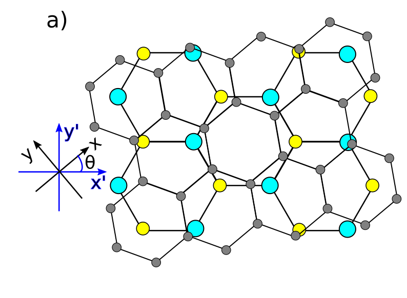
Twisted bilayers In order to obtain the angle we use the methodology recently developed to calculate the coupling strength for graphene/TMDC bilayersDavid et al. (2019). is a quantum phase which depends on the interlayer tunneling between the Bloch states of graphene and the TMDC layer and on certain off-diagonal matrix elements of the intrinsic SOC of the TMDC, for details we refer to Ref. sup . One finds that and are the absolute value and the phase of the complex Rashba coefficient , which is given by the sum of the contributions from pairs of even () and odd () bands of the TMDC: Here and are the magnitude and the phase of the contributions of the pairs of bands. In the calculations of and we have used the tight-binding model of Ref. Fang et al. (2015). For the initial steps of the calculations it is convenient to assume that the graphene layer is rotated with respect to the TMDC layerDavid et al. (2019). In the final steps, we change the representation of the Hamiltonian from the coordinate system fixed to the TMDC layer to the system fixed to the graphene layer with a transformation , see Fig. 1(a). From the explicit form of the transformed Rashba Hamiltonian one finds that the non-zero matrix elements are , i.e., the sum of the geometric angle and the quantum phase plays an important role.
Regarding our numerical calculations, the first ingredient is the tight-binding (TB) Hamiltonian of Ref. Fang et al. (2015) for TMDCs. This TB model itself is derived from density functional theory (DFT) calculations and we use it, among others, to calculate matrix elements of the spin-orbit coupling Hamiltonian and the interlayer tunneling amplitude. The results also depend on i) the position of the Dirac point of graphene within the band gap of the TMDC, and ii) on the value of . Numerical DFT calculations are known to often underestimate and they seem to giveGmitra et al. (2016) different results from experimentsPierucci et al. (2016); Nakamura et al. (2020) for the energy alignment of graphene’s Dirac point with the TMDC bands. We performed our calculations for two parameter sets to assess how sensitive are the results on the choice of these material parameters. Since Ref. Fang et al. (2015) does not provide information on the band alignment of graphene and the TMDC layer, we use the DFT calculations of Ref. Gmitra et al. (2016) for this purpose. The second parameter set for and the band alignment is extracted from ARPES measurementsPierucci et al. (2016); Nakamura et al. (2020). Since the coupling between the layers is weak at the Dirac point of graphene, the band alignment should mainly depend on the work function difference between the two materials. Therefore we assume that it does not depend on the interlayer twist angle. This is in agreement with the recent computational work of Ref. Naimer et al., 2021.
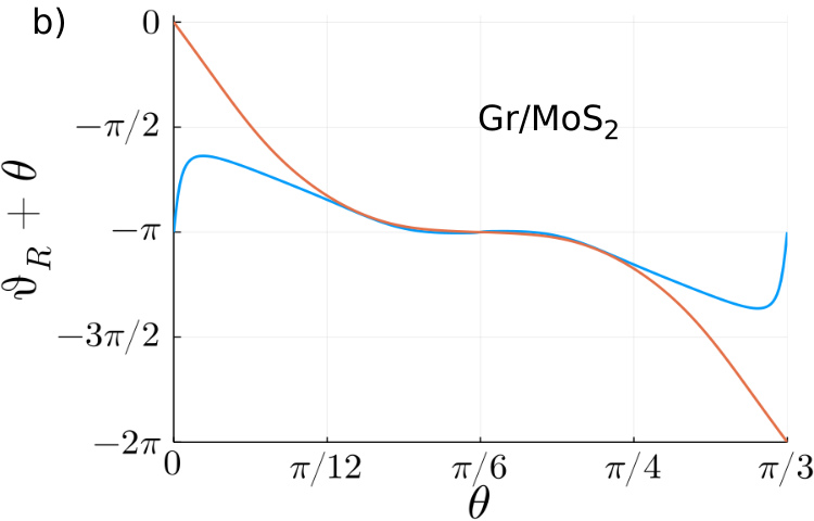
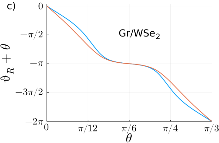
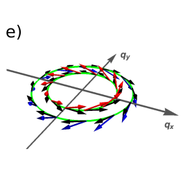
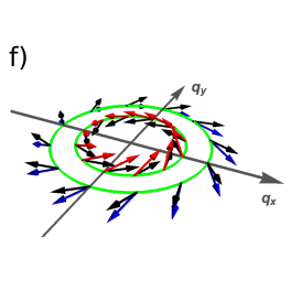
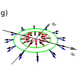
The results for the vs dependence for two selected TMDCs, MoS2 and WSe2, are shown in Figs. 1(b) and (c), respectively. In the case of MoS2, using the DFT parameter set, one can see that remains in a limited range around as varies from to (Fig. 1(b)). However, if parameters extracted from ARPES measurementsPierucci et al. (2016) are used then covers the entire range . For WSe2 one finds that covers all of (Fig. 1(c)) and the results obtained from the two parameter sets qualitatively agree. The difference between the results for the two materials can be mainly traced back to the different energy alignment of the Dirac point in the TMDC band gap. One can also note in Figs. 1(b,c) that for , one finds , where is an integer. We give a detailed discussion of how this result for follows from our theoretical method in Ref. sup , but already note at this point that for the vertical mirror planes of the graphene and the TMDC lattice line up and the system, as a whole, has symmetry. In this case the Hamiltonian of the induced Rashba SOC reads , hence simplifies to the form used previously in the literatureKane and Mele (2005); Gmitra et al. (2016). We find that can be, in general, both odd and even (see Figs. 1(b),(c)), which means that can acquire a negative sign as is changed. Interestingly, when , the spin-orbit field is not tangential to the Fermi surface as in the case of usual Rashba SOC (cf. Fig. 1(e) and Figs. 1(f),(g)). Instead, one can show that the in-plane component is rotated by an angle with respect to the tangential direction. As we will discuss, this might have consequences on the interpretation of experimental results.
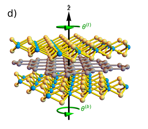
Twisted TMDC/graphene/TMDC trilayers Adding another TMDC layer, as shown in Fig. 1(d), introduces a second interlayer twist angle and the two twist angles and for the bottom and top TMDC layers allow an even broader control of the induced SOC in graphene.
Since the layers are only weakly coupled, the effective graphene Hamiltonian is , where and . Here is the Hamiltonian of the induced valley Zeeman SOC in the graphene layer. Note, that the contributions and have a different sign. As a simple physical explanation, consider the case when the two TMDC layers are perfectly aligned, e.g., . Then the graphene layer is horizontal mirror plane of the whole stack, which dictates that the Rashba SOC must vanish. (A more microscopic argument is given in Ref. sup .) One can define the complex Rashba coefficient for the trilayer system (tls) by
| (2) |
and its magnitude and phase . In terms of these quantities the induced Rashba type SOC can be written as . The importance of the phase discussed for bilayers becomes now more clear: it follows from Eq. (2) that the strength of the induced Rashba SOC in trilayer stacks can be affected by quantum interference effects if and/or are non-zero. This can be interpreted as an interference of the virtual hopping processes to the two TMDC layers that give rise to the induced Rashba SOC.
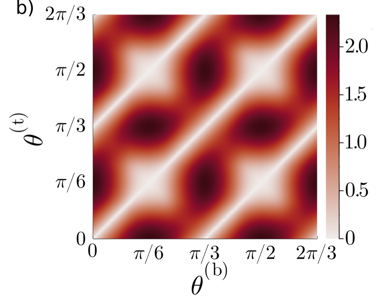
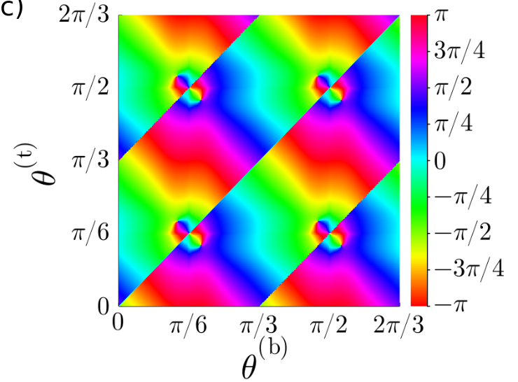
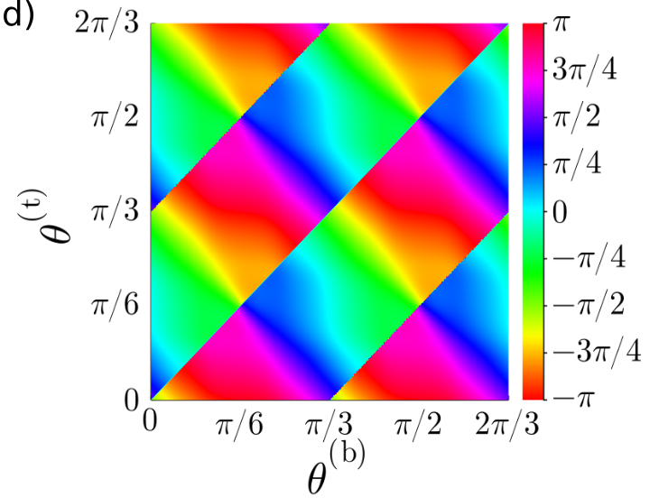
Calculations for the twist angle dependence of have already been performed in Refs. Li and Koshino (2019); David et al. (2019), therefore we do not show these results here, see Ref. sup for further details. The results of our numerical calculations for are summarized in Figs. 2(a)-(d). Firstly, symmetries that are broken in bilayers can be restored in trilayers for certain and angles. If , where is an odd integer, the trilayer stack is inversion symmetric. On the other hand, for an even the stack has a horizontal mirror plane. Therefore the induced Rashba SOC must vanish for any integer , as it can be seen in Figs. 2(a),(b). For WSe2 encapsulation (Fig. 2(a)) the maximum of is found for . The maximum value of is around 70% larger than in the graphene/WSe2 case. Thus, double-sided encapsulation can significantly enhance the induced Rashba SOC. Surprisingly, when using MoS2 for double encapsulation (Fig. 2(b)), we find that basically cannot be enhanced above the value obtained for one sided proximity effect. This can be understood by considering the explicit dependence of and on , see Ref. sup for details. The origin of the extended regions where is very small is due to the fact that for those twist angles and change slowly in both layers and therefore they approximately cancel in Eq. (2). In Figs. 2(c,d) we show the phase of Eq. (2), which determines the winding of the SOC field in the case of double encapsulation. The apparent diagonal lines correspond to where is not defined.
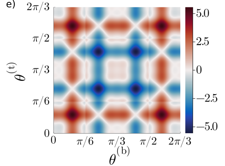
For completeness, we also discuss the twist angle dependence of the induced valley Zeeman SOC in TMDC/graphene/TMDC trilayers, see Figs. 2(e,f). The strength of the valley Zeeman type SOC is simply given by . If the two TMDC layers are (nearly) aligned, they can double the strength of the induced valley Zeeman SOC. When the whole stack has inversion symmetry, the effect of the two layers cancel and . The valley Zeeman SOC also vanishes along the lines , this is a combined effect of time reversal and three-fold rotation symmetry of the TMDC layers. We also note that depends sensitively on what kind of TMDC is used in the stacks. The difference between the effects of WSe2 (Fig. 2(e)) and MoS2(Fig. 2(f)) is mainly due to the different alignment of graphene’s Dirac point with the TMDC bands. The calculations shown in Fig. 2, together with Eq. (2) are the main results of this work.
In the preceding discussions of graphene/TMDC and TMDC/graphene/TMDC heterostructures we have neglected a possible lateral shift of the graphene layer with respect to the TMDCs and moiré effects. Regarding the lateral shift, it does not affect our resultssup . Considering the moiré effects, in graphene/TMDC bilayers they are present only at energy scales larger than 2 eVsup ; Pierucci et al. (2016), i.e., they are negligible for energies close to the Dirac point of graphene. The situation might be different in TMDC/graphene/TMDC trilayers. Based on previous work of Refs. Andjelković et al., 2020; Oka and Koshino, 2021 on hBN/graphene/hBN trilayers, one may expect that supermoiré effects may become important when the TMDC layers are nearly aligned: (see Ref. sup for further details). The discussion of supermoiré is beyond the scope of the present work.
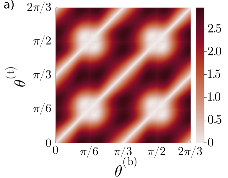
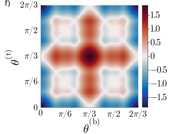
Experimental predictions Several recent works Ghiasi et al. (2017); Benítez et al. (2018); Xu et al. (2018) measured an anisotropy of the out-of-plane and in-plane spin lifetimes in graphene/TMDC heterostructures which can be interpreted as direct proof of induced SOC in graphene. Namely, according to the theoretical calculations of RefCummings et al. (2017), if there is a strong intervalley scattering in graphene, then the ratio of the spin lifetimes is given by , where () is the intervalley (momentum) scattering time. (For ultraclean samples with SOC comparable to or larger than the disorder-induced quasiparticle broadening, a qualitatively different spin relaxation anisotropy is derived in Ref. Offidani and Ferreira (2018).) Let us consider a WSe2/graphene/WSe2 heterostructure and assume that is kept fixed while is changed. Note, that the ratio can be tuned in a wider range in trilayer structures than in bilayers. For example, is never zero for graphene/TMDC whereas one can choose and such that and , see Figs. 2(a),(e). Using as in RefCummings et al. (2017), we plot as a function of for and in Fig. 3(a). When and then becomes small but is finite, therefore strongly increases as a function of . This enhancement happens before supermoiré effects might become important for . In contrast, if then remains finite for all angles. This dramatic difference in the dependence of is clearly a consequence of the wider tunability of in trilayers.
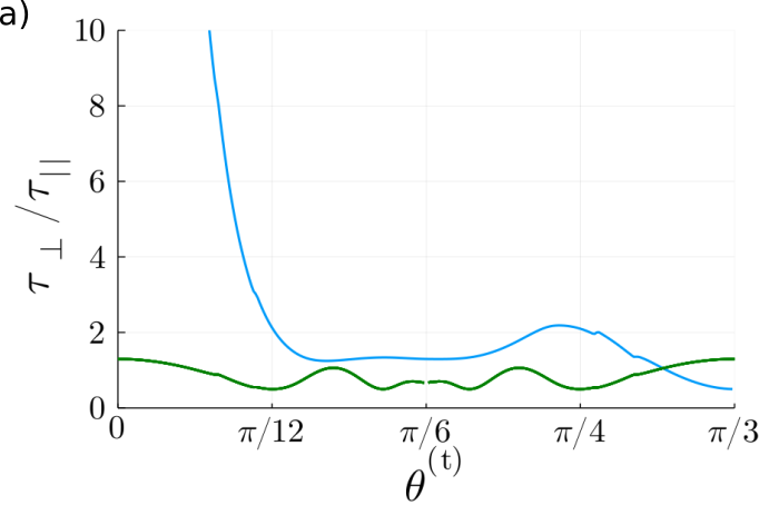
One can expect that charge-to-spin conversion measurements should also be affected by the interlayer twist. Let us consider a graphene/TMDC bilayer and for simplicity assume that i) and ii) a dc electric field is applied along the direction. In steady state the component of the spin density is given by where is the deviation of the quasiparticle distribution with respect to equilibrium. Using the semiclassical argument given in Ref.Offidani et al. (2017), for Fermi energies close to the Dirac point such that , i.e., when there is a single Fermi surface, one finds that . This suggests that the Rashba-Edelstein effect (REE) may vanish (when ) even though is not required to be zero by symmetry for any . can also change sign as a function of the interlayer twist angle, because , see Figs. 1(b),(c). Regarding the more realistic situation when there are two spin-polarized Fermi surfaces in graphene for , looking at Figs. 1(g) one can understand that can be zero as a function of twist angle in this case as well. Furthermore, in twisted TMDC/graphene/TMDC trilayers, the REE can vanish either because or because , which can be expressed compactly as . As an example, the region where this condition is fulfilled in the , space for WSe2/graphene/WSe2 trilayers is shown in Fig. 3(b).
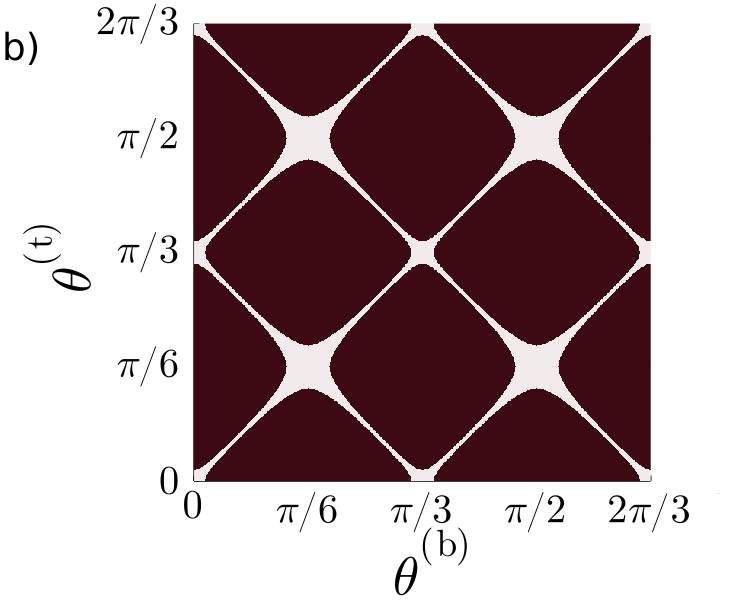
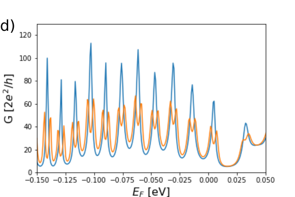
While the spin-lifetime anisotropy measurements require diffusive samples, in Figs. 3 (c)-(d) we show an example of how strong SOC can affect ballistic transport properties. Highly transparent and junctions in graphene have recently been realized in several experimentsYoung and Kim (2009); Rickhaus et al. (2013, 2015); Chen et al. (2016); Handschin et al. (2017); Dauber et al. (2020) and Fabry-Perrot type interference measurementsHandschin et al. (2017); Dauber et al. (2020). Assume now that a TMDC/graphene/TMDC trilayer is tuned with interlayer twist angles such that the Rashba SOC is switched-off and simultaneously the valley Zeeman SOC enhanced. We calculate the conductancesup through a smooth graphene junctionShytov et al. (2008) as a function of out-of-plane magnetic field and Fermi energy for meV, see Fig. 3(c). One can observe that for T the high-conductance ridges are split. This is apparent in Fig. 3(d), where we compare the cases when (blue) and meV (orange) for a fixed magnetic field T. Our calculations also indicate that the Rashba type SOC does not have a similar effect on the conductance ridges (not shown). An additional experimental probe of the twist angle dependent SOC may be the measurement of the reflection of electrons at a planar junction, which is briefly discussed in Ref. sup .
Summary We found that the induced Rashba type SOC in twisted hexagonal bilayers can be parameterized by the strength and a spin-rotation angle . This latter can lead to interference effects for in trilayer heterostructures. We also calculated the valley Zeeman SOC in twisted TMDC/graphene/TMDC trilayers. Finally, we discussed how the interlayer twist angle dependence of the induced SOC can be deduced from spin-lifetime anisotropy, charge-to-spin conversion and magnetrotransport measurements.
In this work we have neglected possible lattice relaxation in vdW heterostructuresSilva et al. (2020). An important future direction would be to study its effect on the results presented here.
Acknowledgments We acknowledge helpful conversations with Péter Makk and Jaroslav Fabian. This research was supported by the Ministry of Innovation and Technology and the National Research, Development and Innovation Office (NKFIH) within the Quantum Information National Laboratory of Hungary. P.R. and A.K. were also supported by the ELTE Institutional Excellence Program (TKP2020-IKA-05), and the Hungarian Scientific Research Fund (OTKA) Grants No.K134437 and No.NN127903 (Topograph FlagERA project). A.K. acknowledges support from the Hungarian Academy of Sciences through the Bolyai János Stipendium (BO/00603/20/11) as well.
Note added During the preparation of this manuscript we have become aware of Ref. Naimer et al. (2021), where the authors discuss the twist angle dependence of the induced SOC in graphene/TMDC structures using DFT calculations.
References
- Yankowitz et al. (2012) M. Yankowitz, J. Xue, D. Cormode, J. D. Sanchez-Yamagishi, K. Watanabe, T. Taniguchi, P. Jarillo-Herrero, P. Jacquod, and B. J. LeRoy, Nature Physics 8, 382 (2012).
- Ponomarenko et al. (2013) L. A. Ponomarenko, R. V. Gorbachev, G. L. Yu, D. C. Elias, R. Jalil, A. A. Patel, A. Mishchenko, A. S. Mayorov, C. R. Woods, J. R. Wallbank, M. Mucha-Kruczynski, B. A. Piot, M. Potemski, I. V. Grigorieva, K. S. Novoselov, F. Guinea, V. I. Fal’ko, and A. K. Geim, Nature 497, 594 (2013).
- Hunt et al. (2013) B. Hunt, J. D. Sanchez-Yamagishi, A. F. Young, M. Yankowitz, B. J. LeRoy, K. Watanabe, T. Taniguchi, P. Moon, M. Koshino, P. Jarillo-Herrero, and R. C. Ashoori, Science 340, 1427 (2013), https://science.sciencemag.org/content/340/6139/1427.full.pdf .
- Ribeiro-Palau et al. (2018) R. Ribeiro-Palau, C. Zhang, K. Watanabe, T. Taniguchi, J. Hone, and C. R. Dean, Science 361, 690 (2018).
- Wang et al. (2015) Z. Wang, D.-K. Ki, H. Chen, H. Berger, A. H. MacDonald, and A. F. Morpurgo, Nat. Comm. 6, 8339 (2015).
- Wang et al. (2016) Z. Wang, D.-K. Ki, J. Y. Khoo, D. Mauro, H. Berger, L. S. Levitov, and A. F. Morpurgo, Phys. Rev. X 6, 041020 (2016).
- Yang et al. (2016) B. Yang, M.-F. Tu, J. Kim, Y. Wu, H. Wang, J. Alicea, R. Wu, M. Bockrath, and J. Shi, 2D Mater. 3, 031012 (2016).
- Bistritzer and MacDonald (2011) R. Bistritzer and A. H. MacDonald, PNAS 108, 12233 (2011).
- Cao et al. (2018) Y. Cao, V. Fatemi, S. Fang, K. Watanabe, T. Taniguchi, E. Kaxiras, and P. Jarillo-Herrero, Nature 556, 43 (2018).
- Arora et al. (2020) H. S. Arora, R. Polski, Y. Zhang, A. Thomson, Y. Choi, H. Kim, Z. Lin, I. Z. Wilson, X. Xu, J.-H. Chu, K. Watanabe, T. Taniguchi, J. Alicea, and S. Nadj-Perge, Nature 583, 379 (2020).
- Lin et al. (2021) J.-X. Lin, Y.-H. Zhang, E. Morissette, Z. Wang, S. Liu, D. Rhodes, K. Watanabe, T. Taniguchi, J. Hone, and J. I. A. Li, (2021), arXiv:2102.06566 [cond-mat.mes-hall] .
- Island et al. (2019) J. O. Island, X. Cui, C. Lewandowski, J. Y. Khoo, E. M. Spanton, H. Zhou, D. Rhodes, J. C. Hone, T. Taniguchi, K. Watanabe, L. S. Levitov, M. P. Zaletel, and A. F. Young, Nature 571, 85 (2019).
- Khoo et al. (2017) J. Y. Khoo, A. F. Morpurgo, and L. Levitov, Nano Letters 17, 7003 (2017), pMID: 29058917, https://doi.org/10.1021/acs.nanolett.7b03604 .
- Gmitra and Fabian (2017) M. Gmitra and J. Fabian, Phys. Rev. Lett. 119, 146401 (2017).
- Wang et al. (2019a) D. Wang, S. Che, G. Cao, R. Lyu, K. Watanabe, T. Taniguchi, C. N. Lau, and M. Bockrath, Nano Letters 19, 7028 (2019a), pMID: 31525877, https://doi.org/10.1021/acs.nanolett.9b02445 .
- Tiwari et al. (2021) P. Tiwari, S. K. Srivastav, and A. Bid, Phys. Rev. Lett. 126, 096801 (2021).
- Wang et al. (2019b) Z. Wang, Y. B. Wang, J. Yin, E. Tóvári, Y. Yang, L. Lin, M. Holwill, J. Birkbeck, D. J. Perello, S. Xu, J. Zultak, R. V. Gorbachev, A. Kretinin, T. Taniguchi, K. Watanabe, S. V. Morozov, M. Andjelković, S. Milovanović, L. Covaci, F. M. Peeters, A. A. Mishchenko, A. K. Geim, K. S. Novoselov, V. I. Fal’ko, A. Knothe, and C. R. Woods, Science Advances 5, eaay8897 (2019b).
- Zhu et al. (2020) Z. Zhu, P. Cazeaux, M. Luskin, and E. Kaxiras, Phys. Rev. B 101, 224107 (2020).
- Wang et al. (2019c) L. Wang, S. Zihlmann, M.-H. Liu, P. Makk, K. Watanabe, T. Taniguchi, A. Baumgartner, and C. Schönenberger, Nano Letters 19, 2371 (2019c), pMID: 30803238, https://doi.org/10.1021/acs.nanolett.8b05061 .
- Kennes et al. (2021) D. M. Kennes, M. Claassen, L. Xian, A. Georges, A. J. Millis, J. Hone, C. R. Dean, D. N. Basov, A. N. Pasupathy, and A. Rubio, Nature Physics 17, 155 (2021).
- Yang et al. (2017) B. Yang, M. Lohmann, D. Barroso, I. Liao, Z. Lin, Y. Liu, L. Bartels, K. Watanabe, T. Taniguchi, and J. Shi, Phys. Rev. B 96, 041409(R) (2017).
- Völkl et al. (2017) T. Völkl, T. Rockinger, M. Drienovsky, K. Watanabe, T. Taniguchi, D. Weiss, and J. Eroms, Phys. Rev. B 96, 125405 (2017).
- Zihlmann et al. (2018) S. Zihlmann, A. W. Cummings, J. H. Garcia, M. Kedves, K. Watanabe, T. Taniguchi, C. Schönenberger, and P. Makk, Phys. Rev. B 97, 075434 (2018).
- Wakamura et al. (2018) T. Wakamura, F. Reale, P. Palczynski, S. Guéron, C. Mattevi, and H. Bouchiat, Phys. Rev. Lett. 120, 106802 (2018).
- Wakamura et al. (2019) T. Wakamura, F. Reale, P. Palczynski, M. Q. Zhao, A. T. C. Johnson, S. Guéron, C. Mattevi, A. Ouerghi, and H. Bouchiat, Phys. Rev. B 99, 245402 (2019).
- Ghiasi et al. (2017) T. S. Ghiasi, J. Ingla-Aynés, A. A. Kaverzin, and B. J. van Wees, Nano Lett. 17, 7528 (2017).
- Leutenantsmeyer et al. (2018) J. C. Leutenantsmeyer, J. Ingla-Aynés, J. Fabian, and B. J. van Wees, Phys. Rev. Lett. 121, 127702 (2018).
- Benítez et al. (2018) L. A. Benítez, J. F. Sierra, W. S. Torres, A. Arrighi, F. Bonell, M. V. Costache, and S. O. Valenzuela, Nature Physics 14, 303 (2018).
- Xu et al. (2018) J. Xu, T. Zhu, Y. K. Luo, Y.-M. Lu, and R. K. Kawakami, Phys. Rev. Lett. 121, 127703 (2018).
- Safeer et al. (2019) C. K. Safeer, J. Ingla-Aynés, F. Herling, J. H. Garcia, M. Vila, N. Ontoso, M. R. Calvo, S. Roche, L. E. Hueso, and F. Casanova, Nano Lett. 19, 1074 (2019).
- Herling et al. (2020) F. Herling, C. K. Safeer, J. Ingla-Aynés, N. Ontoso, L. E. Hueso, and F. Casanova, APL Materials 8, 071103 (2020), https://doi.org/10.1063/5.0006101 .
- Benítez et al. (2020) L. A. Benítez, W. Savero Torres, J. F. Sierra, M. Timmermans, J. H. Garcia, S. Roche, M. V. Costache, and S. O. Valenzuela, Nature Materials 19, 170 (2020).
- Hoque et al. (2020) A. M. Hoque, D. Khokhriakov, B. Karpiak, and S. P. Dash, Phys. Rev. Research 2, 033204 (2020).
- Ghiasi et al. (2019) T. S. Ghiasi, A. A. Kaverzin, P. J. Blah, and B. J. van Wees, Nano Letters 19, 5959 (2019), pMID: 31408607, https://doi.org/10.1021/acs.nanolett.9b01611 .
- Khokhriakov et al. (2020) D. Khokhriakov, A. M. Hoque, B. Karpiak, and S. P. Dash, Nature Communications 11, 3657 (2020).
- Li et al. (2020) L. Li, J. Zhang, G. Myeong, W. Shin, H. Lim, B. Kim, S. Kim, T. Jin, S. Cavill, B. S. Kim, C. Kim, J. Lischner, A. Ferreira, and S. Cho, ACS Nano 14, 5251 (2020), pMID: 32267673, https://doi.org/10.1021/acsnano.0c01037 .
- Gmitra et al. (2016) M. Gmitra, D. Kochan, P. Högl, and J. Fabian, Phys. Rev. B 93, 155104 (2016).
- Milletarì et al. (2017) M. Milletarì, M. Offidani, A. Ferreira, and R. Raimondi, Phys. Rev. Lett. 119, 246801 (2017).
- Cummings et al. (2017) A. W. Cummings, J. H. Garcia, J. Fabian, and S. Roche, Phys. Rev. Lett. 119, 206601 (2017).
- Garcia et al. (2017) J. H. Garcia, A. W. Cummings, and S. Roche, Nano Letters 17, 5078 (2017), pMID: 28715194, https://doi.org/10.1021/acs.nanolett.7b02364 .
- Offidani et al. (2017) M. Offidani, M. Milletarì, R. Raimondi, and A. Ferreira, Phys. Rev. Lett. 119, 196801 (2017).
- Garcia et al. (2018) J. H. Garcia, M. Vila, A. W. Cummings, and S. Roche, Chem. Soc. Rev. 47, 3359 (2018).
- Gani et al. (2020) Y. S. Gani, E. J. Walter, and E. Rossi, Phys. Rev. B 101, 195416 (2020).
- Cavill et al. (2020) S. A. Cavill, C. Huang, M. Offidani, Y.-H. Lin, M. A. Cazalilla, and A. Ferreira, Phys. Rev. Lett. 124, 236803 (2020).
- Zollner and Fabian (2021) K. Zollner and J. Fabian, (2021), arXiv:2103.15378 [cond-mat.mes-hall] .
- Alsharari et al. (2018) A. M. Alsharari, M. M. Asmar, and S. E. Ulloa, Phys. Rev. B 98, 195129 (2018).
- Li and Koshino (2019) Y. Li and M. Koshino, Phys. Rev. B 99, 075438 (2019).
- David et al. (2019) A. David, P. Rakyta, A. Kormányos, and G. Burkard, Phys. Rev. B 100, 085412 (2019).
- Pezo et al. (2020) A. Pezo, Z. Zanolli, N. Wittemeier, A. Fazzio, S. Roche, and J. H. Garcia, (2020), arXiv:2011.06714 [cond-mat.mes-hall] .
- Kane and Mele (2005) C. L. Kane and E. J. Mele, Phys. Rev. Lett. 95, 226801 (2005).
- Min et al. (2006) H. Min, J. E. Hill, N. A. Sinitsyn, B. R. Sahu, L. Kleinman, and A. H. MacDonald, Phys. Rev. B 74, 165310 (2006).
- Konschuh et al. (2010) S. Konschuh, M. Gmitra, and J. Fabian, Phys. Rev. B 82, 245412 (2010).
- Zollner et al. (2021) K. Zollner, A. W. Cummings, S. Roche, and J. Fabian, Phys. Rev. B 103, 075129 (2021).
- Yang et al. (2020) X. Yang, B. Sa, P. Lin, C. Xu, Q. Zhu, H. Zhan, and Z. Sun, The Journal of Physical Chemistry C 124, 23699 (2020), https://doi.org/10.1021/acs.jpcc.0c06890 .
- Zollner et al. (2020) K. Zollner, M. D. Petrović, K. Dolui, P. Plecháč, B. K. Nikolić, and J. Fabian, Phys. Rev. Research 2, 043057 (2020).
- Zollner and Fabian (2019) K. Zollner and J. Fabian, Phys. Rev. B 100, 165141 (2019).
- Kandrai et al. (2020) K. Kandrai, P. Vancsó, G. Kukucska, J. Koltai, G. Baranka, Ákos Hoffmann, Áron Pekker, K. Kamarás, Z. E. Horváth, A. Vymazalová, L. Tapasztó, and P. Nemes-Incze, Nano Letters 20, 5207 (2020), pMID: 32551708, https://doi.org/10.1021/acs.nanolett.0c01499 .
- Fülöp et al. (2021) B. Fülöp, A. Márffy, S. Zihlmann, M. Gmitra, E. Tóvári, B. Szentpéteri, M. Kedves, K. Watanabe, T. Taniguchi, J. Fabian, C. Schönenberger, P. Makk, and S. Csonka, (2021), arXiv:2103.13325 [cond-mat.mes-hall] .
- (59) see Supplementary information .
- Fang et al. (2015) S. Fang, R. Kuate Defo, S. N. Shirodkar, S. Lieu, G. A. Tritsaris, and E. Kaxiras, Phys. Rev. B 92, 205108 (2015).
- Pierucci et al. (2016) D. Pierucci, H. Henck, J. Avila, A. Balan, C. H. Naylor, G. Patriarche, Y. J. Dappe, M. G. Silly, F. Sirotti, A. T. C. Johnson, M. C. Asensio, and A. Ouerghi, Nano Letters 16, 4054 (2016).
- Nakamura et al. (2020) H. Nakamura, A. Mohammed, P. Rosenzweig, K. Matsuda, K. Nowakowski, K. Küster, P. Wochner, S. Ibrahimkutty, U. Wedig, H. Hussain, J. Rawle, C. Nicklin, B. Stuhlhofer, G. Cristiani, G. Logvenov, H. Takagi, and U. Starke, Phys. Rev. B 101, 165103 (2020).
- Naimer et al. (2021) T. Naimer, K. Zollner, M. Gmitra, and J. Fabian, Phys. Rev. B 104, 195156 (2021).
- (64) We describe the energy of the Dirac point of graphene in the band gap of the TMDC by a number . Its value is a linear function of the position of the Dirac point in the TMDC band gap. When , the Dirac point is aligned with the TMDC valence band edge, for the Dirac point has the same energy as the TMDC conduction band edge. In the calculations involving MoS2, we used DFT parameters eV, and experimental parametersPierucci et al. (2016) eV, . In the case of WSe2, DFT parameters were eV, and experimental onesNakamura et al. (2020) eV, .
- Andjelković et al. (2020) M. Andjelković, S. P. Milovanović, L. Covaci, and F. M. Peeters, Nano Letters 20, 979 (2020), pMID: 31961161, https://doi.org/10.1021/acs.nanolett.9b04058 .
- Oka and Koshino (2021) H. Oka and M. Koshino, Phys. Rev. B 104, 035306 (2021).
- Offidani and Ferreira (2018) M. Offidani and A. Ferreira, Phys. Rev. B 98, 245408 (2018).
- Young and Kim (2009) A. F. Young and P. Kim, Nature Physics 5, 222 (2009).
- Rickhaus et al. (2013) P. Rickhaus, R. Maurand, M.-H. Liu, M. Weiss, K. Richter, and C. Schönenberger, Nature Communications 4, 2342 (2013).
- Rickhaus et al. (2015) P. Rickhaus, P. Makk, M.-H. Liu, E. Tóvári, M. Weiss, R. Maurand, K. Richter, and C. Schönenberger, Nature Communications 6, 6470 (2015).
- Chen et al. (2016) S. Chen, Z. Han, M. M. Elahi, K. M. M. Habib, L. Wang, B. Wen, Y. Gao, T. Taniguchi, K. Watanabe, J. Hone, A. W. Ghosh, and C. R. Dean, Science 353, 1522 (2016), https://science.sciencemag.org/content/353/6307/1522.full.pdf .
- Handschin et al. (2017) C. Handschin, P. Makk, P. Rickhaus, M.-H. Liu, K. Watanabe, T. Taniguchi, K. Richter, and C. Schönenberger, Nano Letters 17, 328 (2017), https://doi.org/10.1021/acs.nanolett.6b04137 .
- Dauber et al. (2020) J. Dauber, K. J. A. Reijnders, L. Banszerus, A. Epping, K. Watanabe, T. Taniguchi, M. I. Katsnelson, F. Hassler, and C. Stampfer, (2020), arXiv:2008.02556 [cond-mat.mes-hall] .
- Shytov et al. (2008) A. V. Shytov, M. S. Rudner, and L. S. Levitov, Phys. Rev. Lett. 101, 156804 (2008).
- Silva et al. (2020) A. Silva, V. E. P. Claerbout, T. Polcar, D. Kramer, and P. Nicolini, ACS Applied Materials & Interfaces 12, 45214 (2020), pMID: 32894936, https://doi.org/10.1021/acsami.0c13971 .