Two-Terminal Tandem Solar Cells based on Perovskite and Transition Metal Dichalcogenides
Abstract
Perovskite solar cells have shown power conversion efficiencies (PCE) comparable to cystalline silicon solar cell despite involving low-temperature, solution based synthesis processes outside clean room environment. As the theoretical PCE of a perovskite solar cell with band gap 1.55 eV is capped to 33 % due to Shockley–Queisser limit, tandem configurations are being investigated to go beyond this limit. Here, we propose a two-terminal (2T) tandem solar cell structure consisting of perovskite and multilayer transition metal dichalcogenide as the absorber layers of the top and the bottom subcells, respectively and investigate their performance parameters using Solar Cell Capacitance Simulator-1 Dimension (SCAPS-1D) software package. We demonstrate that the 2T tandem solar cell consisting of CH3NH3PbI3 with band gap 1.55 eV and MoTe2 with bandgap 1.1 eV shows PCE of maximum 35.3 % under AM 1.5 G illumination. This work motivates experimental realization of such solar cells for further investigation.
keywords:
Perovskites, TMDCs, MoTe2 Tandem Solar cells, SCAPS-1D, 2-Terminal monolithic, SimulationIntroduction
Perovskite based solar cells have seen significant rise in solar efficiency in less than a decade since 2012 1, 2, 3. They are attractive as they involve low-temperature, solution and vapor-phase based fabrication processes using low cost precursors 4, 5 without the requirement of cleanroom facilities compared to fabrication of conventional silicon based solar cells. The high power conversion efficiency (PCE) in the perovskite solar cells are attributed to higher charge carriers mobility 6, long carrier diffusion lengths 7, high absorption coefficients 8 and tuneable energy band gap 9. These properties have led to a remarkable PCE of greater than 25 % in case of single junction perovskite solar cells 10, 3. Even though perovskite based solar cells are promising, their efficiency is capped by the theoretical Shockley-Queisser limit (PCE = 33 % for perovskite of band gap 1.34 eV 11). Therefore, tandem solar cell architectures are being investigated to surpass this limit 12, 13, 14.
Tandem solar cell structure consists of two junctions in series with higher band gap material forming the top junction and lower band gap material forming the bottom junction 12, 13. Here, we are interested in two-terminal (2T) tandem solar cell which require less number of functional layers compared to the four-terminal tandem solar cells. This leads to low optical and electrical losses resulting into economical solar cells. Tunable band gap of the perovskites allows to synthesize all-perovskite tandem solar cells with maximum experimental reported PCE of 24.8 % 15. However, all-pervoskite tandem solar cells suffer from stability problems of low-band gap, bottom layer perovskite along with the migration and mixing of extremely mobile ions within the top and the bottom layers 13. Similarly, tandem solar cell based on perovskites and copper indium gallium selenide (CIGS) also suffer from major challenge of commercialization due to scarcity of gallium and indium 16.
Another notable example of 2T tandem solar cell consists of perovskite as top layer and silicon substrates as the bottom layer. Recently, Al-Ashouri et al. 17 reported a maximum efficiency of 30 % for such a tandem solar consisting of Cs0.05(FA0.77MA0.23)0.95Pb(I0.77Br0.23)3 as the top subcell and silicon heterojunction as the bottom subcell. Such high efficiency has been attributed to a fast and efficient hole-extracting self-assembled monolayer which minimizes non-radiative carrier recombination and also forms lossless interface between the indium tin oxide (ITO) and the perovskite layer. However, the solid and rigid properties of silicon substrates will render perovskite-Si based tandem structure unsuitable for flexible substrate solar cells applications for which perovskites based solar cells have gained some attraction.
Here, we propose a 2T tandem solar cell structures consisting of perovskite and Transition Metal Dichalcogenides (TMDCs) as absorber layers for the top and bottom subcells, respectively and explore its performance parameters. TMDCs are layered crystals which exhibit diverse electrical properties ranging from metallic, semiconducting, ferromagnetic to superconducting phases 18, 19. TMDCs such as MoTe2, MoS2, MoSe2, WS2, and WSe2 are semiconductors and possess excellent optoelectronic properties including large absorption coefficient over broad wavelength spectrum 20, 21. Experimental demonstration of multilayer MoS2 22 and MoSe2 23 as photovoltaics exhibits potential for their use in solar cell applications. Further, they are highly stable in ambient condition and can be grown using various techniques such as chemical vapor transport 24, chemical vapour deposition 25, and hydrothermal technique 26. However, their applications in solar cells require synthesis of multilayer, large area TMDCs to be improved and optimized for large area applications.
The band-gap tuneability, excellent optical properties of both perovskite and TMDCs makes it imperative to investigate performance parameters of 2T tandem solar cell consisting of perovskite and TMDCs as absorber layers of the top and bottom subcells. We use Solar Cell Capacitance Simulator-1 Dimension (SCAPS-1D; version 3.3.08) software package for simulation and study of the single junction and 2T tandem structure solar cells 27. We find that the maximum PCE of the optimized tandem structure is 35.3 % for perovskite of band gap 1.55 eV and MoTe2 having band gap of 1.1 eV. Flexibility of the TMDCs and high absorption coefficient will make this structure attractive for various large-scale applications where thin solar cells can be manufactured in flexible substrates through roll-to-roll-based technologies. Our results provide a motivation for experimental realization of such solar cells for further investigation.
Results and Discussion
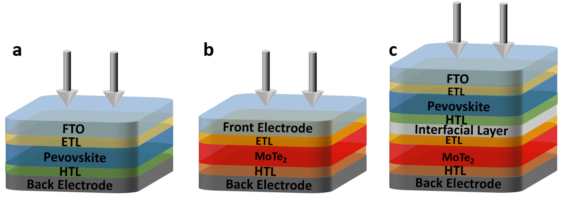
Figure 1 shows schematics of two single junction solar cells containing perovskite and MoTe2 as absorber layers and a 2T tandem solar cell structure containing both absorber layers. The light is incident through the top transparent layer as indicated by the arrows and the bottom layer corresponds to the back electrode. Fig. 1(a) shows arrangement of different layers in single junction perovskite solar cell. It constitutes of top and bottom layers as flourine-doped tin oxide (FTO) and metal electrodes, respectively and electron transport layer (ETL) and hole transport layer (HTL) of TiO2 (thickness = 50 nm) and Cu2O (thickness = 50 nm), respectively. The choice of TiO2 as ETL layer is owing to its appropriate energy level which is suitable for electron injection and hole blocking. TiO2 thin film’s conductance and mobility can further be enhanced by doping with various elements which tend to improve the device performance 28. Similarly, Cu2O has been chosen as HTL because of its appropriate energy level alignment, high hole mobility, and longer lifetime of photo-excited carriers 29. Both the ETL and HTL layers play important role in PCE of perovskite solar cells. ETL and HTL provide low resistance path for charge carriers generated in the absorber layer. Consequently, doping concentration of ETL and HTL layer does not affects the performance of solar cell significantly. Further, with the increase of the thickness of ETL and HTL layers, the performance of solar cell also nearly remains constant 30. As few tens of nm of ETL and HTL give best performance results, we have chosen them to be 50 nm in thickness 31, 32. Important material parameters attributed to the various ETL and HTL layers are similar to as reported by Patel et al. 31 as shown in Table 1. The active layer is the perovksite layer with composition CH3NH3PbI3 and band gap of 1.55 eV while the thickness is varied. Here,the carrier mobility parameters have been taken from Hima et al. 33. We have chosen this composition and the bandgap as the perovskites around this bandgap show high spectral intensity and high stability under illumination 34, 35. Further, the absorption coefficient data for the perovskite layer has been taken from the SCAPS-1D library.
![[Uncaptioned image]](/html/2110.13780/assets/Table1.png)
Similarly, Fig. 1(b) shows arrangement of various layers in single junction solar cell containing MoTe2. It constitutes of top and bottom layers as metal electrodes and ZnO (bandgap = 3.3 eV; thickness = 100 nm as taken from Hao et al. 36) and Cu2Te (bandgap = 1.18 eV; thickness = 80 nm) as ETL and HTL/Back Surface Field layers, respectively. The active layer consists of MoTe2 with the band gap 1.1 eV with the material parameters taken from Faisal et al. 37. Further, the absorption coefficient data for the MoTe2 layer has been taken to have square root dependence with respect to energy. Fig. 1(c) shows arrangement of various layers in the pervoskite and MoTe2 based 2T tandem solar cell. It constitutes of top and bottom subcells with as metal electrodes, ETL and HTL layers corresponding to the respective perovskite and MoTe2 single junction solar cells. In addition, an interfacial layer such as any of TiO2, ITO (Indium Tin oxide), and IZO (Indium Zinc oxide) can be used between the two subcells 14. This layer allows current of the opposite polarity charge carriers from the two subcells to recombine here. Therefore, a current density matching between the top and bottom subcell is required for 2T tandem configuration solar cells.
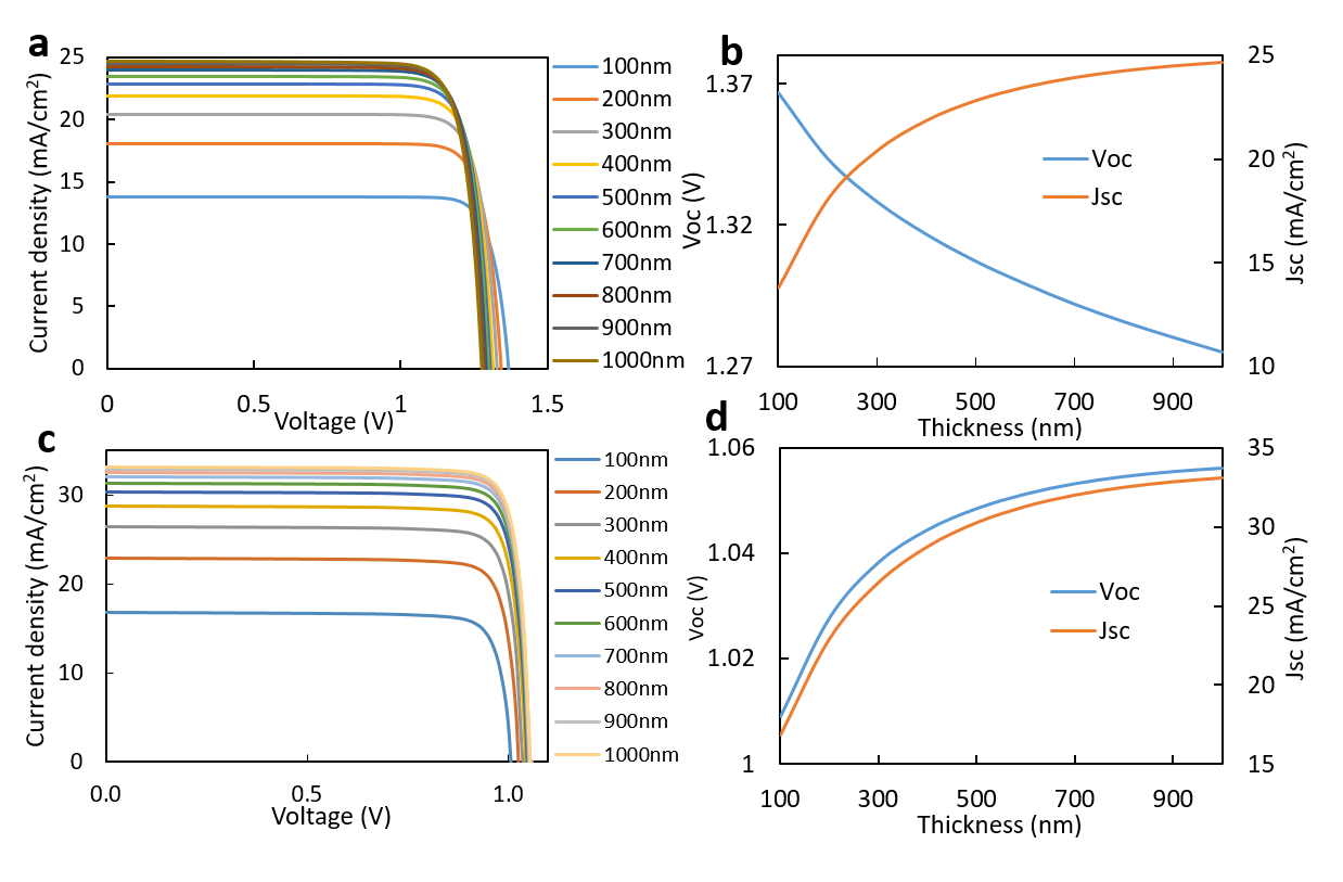
We carry out the simulation of the single junction solar cell containing CH3NH3PbI3 layer using SCAPS-1D software under unfiltered AM 1.5 G illumination. SCAPS-1D is used to simulate and study various kind of single junction and tandem solar cells 31, 38, 34. All the simulations have been performed at temperature 300 K. Further, the losses due to the reflection at interfaces as well as series resistance of the device have not been taken into consideration. Fig. 2(a) show current density vs voltage (J-V) curves for the perovskite single cell for various thickness of the absorber layer. The thickness of the absorber layer has been varied from 100 nm to 1000 nm while keeping other optimized parameters the same as in table 1. We observe that with increasing thickness, the short circuit current density, Jsc, increases with the thickness of the perovskite layer while the value of open circuit voltage, Voc, decreases as shown in Fig. 2(b). As the thickness increases from 100 nm to 1000 nm, Jsc gets nearly doubled while saturating at higher thickness and Voc decreases by 10 % monotonically. The decrease in Voc may be attributed to higher recombination rates of the charge carriers with increasing thickness asd. On the other hand, the initial increase in Jsc is attributed to the increase in the active absorber volume which results in enhanced generation of charge carriers. But, with further increase of thickness, Jsc stays the same due to enhanced layer resistance and carrier recombination. In this calculation, we have kept the acceptor doping concentration of the absorber layer to be 1015 cm-3. Higher doping density will decrease both the Jsc as well as power conversion efficiency (PCE) of the solar cell due to enhanced recombination rate leading to decrease in the minority charge carriers 31, 39. Further, we have assumed the interfaces between the perovskite and neighbouring layers to be defect free.
Next, we perform simulation of the single junction solar cell containing MoTe2 as absorber layer as shown in Fig. 1(b) under unfiltered AM 1.5 G illumination. As earlier, the other parameters of the cell has been kept fixed as shown in Table 1 while the thickness of MoTe2 is varied. Fig. 2(c) shows J Vs V curves for various thickness of the absorber layer. Similar to the single perovskite solar cell, thickness of MoTe2 layer seems to influence performance of solar cells significantly. Here too, the value of Jsc nearly doubles as the thickness of the MoTe2 layer is increased from 100 nm to 1000 nm. On the other hand, Voc is in the range of 1.02 V which is lower than the single junction perovskite solar cell due to the lower band gap of MoTe2 layer. Even though the change in the Voc is significantly small, it increases with increasing thickness due to higher doping concentration of MoTe2 layer. The increase in Jsc initially and saturating at larger thickness is again due to enhanced increase in active absorber volume. Since, the saturation of Jsc is related to charge carrier diffusion length, it tends to saturate at nearly 600 nm. The recombination rate will be significantly higher for the absorber layer having thickness more than 600 nm.
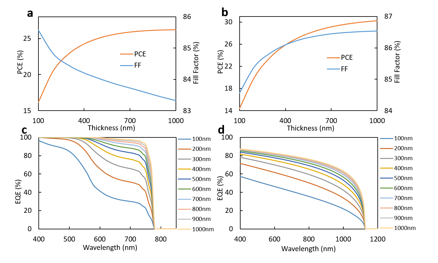
As evident from Fig. 2(a and c), the absorber layer thickness has strong effect on the Fill Factor (FF) and PCE of the two single junction solar cells as shown in Fig. 3. We observe that the PCE of the perovskite solar increases as the thickness of the absorber layer increases and saturates to 25 % at the thickness of 600 nm. This may be attributed to the enhanced absorption of photons leading to generation of charge carriers as the thickness of the abosrber layer increases. However for the thickness approximately more than 600 nm, the unwanted recombination starts to take over which leads to either saturation or the lowering of the PCE. The critical thickness of the absorber layer is related to the diffusion length of the charge carriers. This is consistent with the experimental demonstration of the PCE of the perovskite solar cell 40. The value of the FF decreases with the increasing thickness however the relative change is not significant.
The PCE of single junction MoTe2 solar cell seems to increase with increasing thickness and saturates and 30 % at 1000 nm as shown in Fig. 3(b). We should note that there is no experimental demonstration of solar cell containing MoTe2 as an absorber layer. Therefore, it will be interesting to experimentally realize solar cell based on MoTe2 to measure its PCE and the other performance parameters. On the other hand, Memaran et al. 23 have reported experimental demonstration of single junction solar cells containing multilayer MoS2 in field effect transistor (FET) geometry with efficiency 2.8 %. Further experimental investigation is required to synthesize TMDC based solar cells and enhance their performance parameters.
Figure 3(c) shows dependence of external quantum efficiency (EQE) on the thickness of the absorber layer of the single junction perovskite solar cell. The shape of the EQE is attributed to variation of the refractive index of the perovskite layer on the wavelength of the light which affects the reflecting properties of the layer 41. Further, as the thickness of the absorber layer is increased, EQE increases and acquires a step shape at higher thickness. The edge of the step at 800 nm marks 1.55 eV, the band gap of the CH3NH3PbI3 layer used in the solar cell. Compared to single junction perovskite solar cell, EQE of the MoTe2 solar cell (Fig. 3(d)) shows slightly different dependence with the wavelength which may be attributed to the wavelength dependent refractive index of the material. However, EQE of MoTe2 solar cell remains lower than that of the perovskite solar cell. Further, EQE of the MoTe2 solar cell also increases with the increase in the thickness of the MoTe2 layer with the step at 1125 nm which marks the band gap of MoTe2. 42. Relatively lower EQE of MoTe2 cell limits the current density of the bottom subcell in tandem geometry as discussed later.
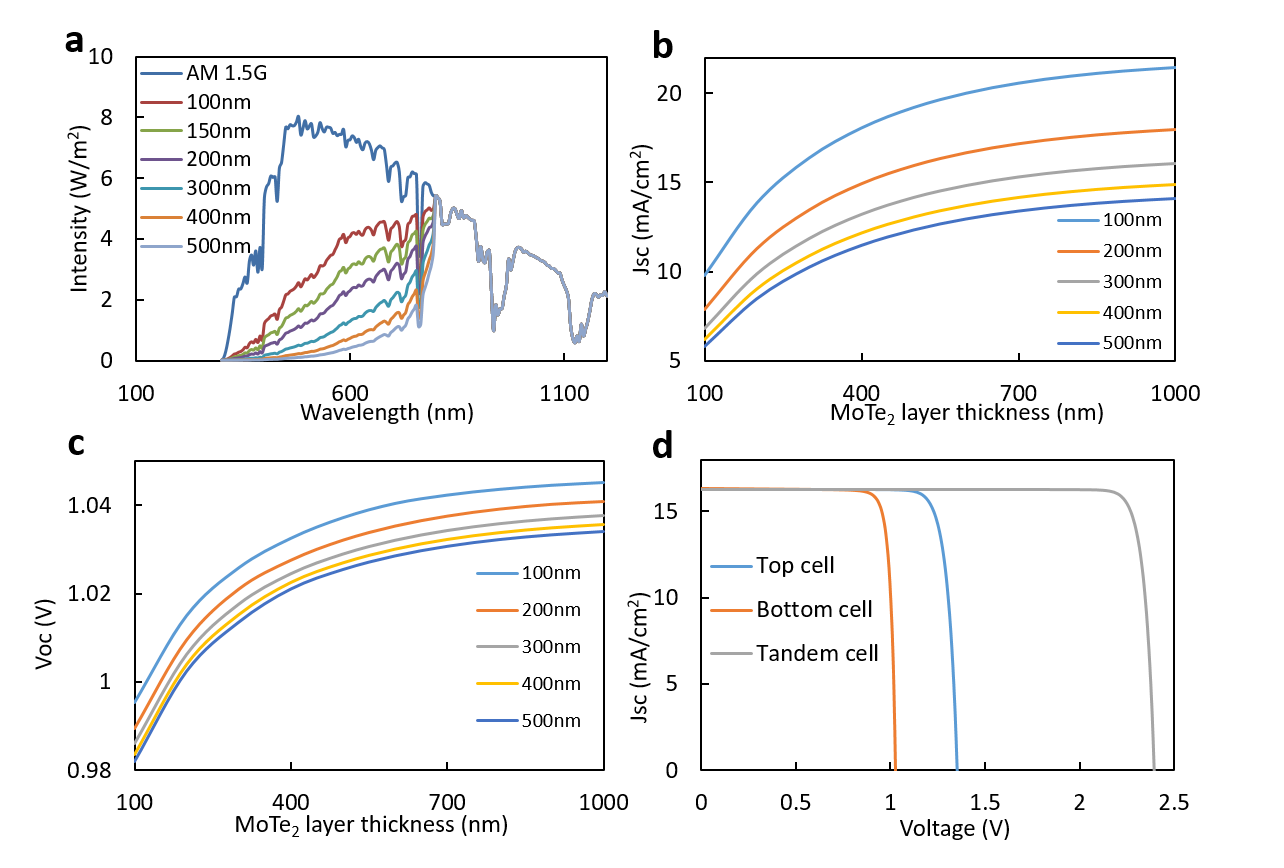
As SCAPS-1D software (version 3.3.08) does not support simulation of 2T tandem solar cell structures, we employ the general technique where the top subcell is analyzed first using standard, unfiltered AM 1.5G spectrum and the filtered spectrum after the top subcell is used to illuminate the bottom subcell 43, 34. Figure 4(a) shows power dependence of the transmitted spectrum on the thickness of CH3NH3PbI3 layer following the top subcell. Above the wavelength higher than 800 nm corresponding to the band gap of CH3NH3PbI3 layer, the active layer remains transparent and all the power gets transmitted. Further, between 500 nm and 800 nm wavelength, we see that the transmitted power varies with the thickness of the absorber layer depending on amount of active volume available for absorption. We use this filtered spectrum to illuminate the bottom subcell and perform further calculations. Fig. 4(b and c) shows the variation of Jsc and Voc extracted from J-V curves as function of thickness of the MoTe2 layer as illuminated by the filtered spectrum for various thickness of top subcell absorber layer. As expected, for a higher thickness of the top subcell active layer, the filtered spectrum will have lower intensities and therefore it will give rise to lower values of Jsc and Voc for the bottom subcell. This indicates a trade-off between the current densities of the two subcells against their thickness. Further, for the tandem solar cell, the final current density is limited by the smaller of the two, therefore, we choose appropriate thickness of the two cells to achieve a current density matching. Fig. 4(d) shows J-V plot for the current density matched top subcell, bottom subcell and 2T tandem solar cell. The current matching condition has been achieved for thickness of 150 nm and 407 nm for CH3NH3PbI3 and MoTe2 layers, respectively which correspond to the current density of 16.3 mA/cm2. Here, the final Voc is 2.4 V and the FF is 90.3. The calculated efficiency is 35.3 % which is significantly higher than the individual single junction solar cells. For comparative analysis, we have also investigated 2T tandem solar cells containing WS2 and WSe2 as bottom subcells (see Supplementary Information Table S1). Among all the tandem solar cell proposed, tandem structure with perovskite and MoTe2 as the absorber layers of top and bottom subcells show the highest efficiency of 35.3 %.
| bandgap (eV) | thickness (nm) | Voc (V) | Jsc (mA/cm2) | FF (%) | PCE (%) | |
| PVK | 1.55 | 1000 | 1.27 | 24.7 | 83.3 | 26.2 |
| MoTe2 | 1.1 | 1000 | 1.05 | 33.1 | 86.5 | 30.3 |
| PVK/MoTe2 | 1.55/1.1 | 150/407 | 2.4 | 16.3 | 90.3 | 35.3 |
Conclusions
We have proposed various 2T tandem solar cells consisting of CH3NH3PbI3 and TMDCs as absorber layers of the top and bottom subcells and have analysed their performance parameters by using SCAPS-1D software package. Single junction perovskite and MoTe2 solar cells have maximum PCE of 26.2 % and 30.3 %, respectively for the optimized material parameters and layer thicknesses of 1000 nm. On the other hand 2T tandem structure can achieve PCE of 35.3 % which is significantly higher than either single junction solar efficiencies. Such high PCEs indicate that perovskite and TMDCs based solar cells are interesting for experimental investigation and carry the potential to be used for manufacturing on flexible substrates through roll-to-roll based technologies.
Two-Terminal Tandem Solar Cells based on Perovskite and Transition Metal Dichalcogenides
We thank Dr. Rajan Jha, IIT Bhubaneswar for discussions. This research was supported by the Department of Science and Technology (SERB – CRG/2020/004293). Further, the authors are thankful to Marc Burgelman and his team at the Electronics and Information Systems (ELIS), University of Gent, Belgium for providing access to SCAPS-1D software package. The authors declare no competing financial interest.
References
- Kojima et al. 2009 Kojima, A.; Teshima, K.; Shirai, Y.; Miyasaka, T. Organometal Halide Perovskites as Visible-Light Sensitizers for Photovoltaic Cells. J. Am. Chem. Soc. 2009, 131, 6050–6051
- Park 2020 Park, N.-G. Research Direction toward Scalable, Stable, and High Efficiency Perovskite Solar Cells. Adv. Energy Mater. 2020, 10, 1903106
- 3 National Renewable Energy Laboratory, Best Research-Cell Efficiency Chart. www.nrel.gov/pv/cell-efficiency.html.
- Yang et al. 2017 Yang, M.; Li, Z.; Reese, M. O.; Reid, O. G.; Kim, D. H.; Siol, S.; Klein, T. R.; Yan, Y.; Berry, J. J.; van Hest, M. F. A. M.; Zhu, K. Perovskite ink with wide processing window for scalable high-efficiency solar cells. Nature Energy 2017, 2, 17038
- Momblona et al. 2016 Momblona, C.; Gil-Escrig, L.; Bandiello, E.; Hutter, E. M.; Sessolo, M.; Lederer, K.; Blochwitz-Nimoth, J.; Bolink, H. J. Efficient vacuum deposited p-i-n and n-i-p perovskite solar cells employing doped charge transport layers. Energy Environ. Sci. 2016, 9, 3456–3463
- Herz 2017 Herz, L. M. Charge-Carrier Mobilities in Metal Halide Perovskites: Fundamental Mechanisms and Limits. ACS Energy Lett. 2017, 2, 1539–1548
- Xing et al. 2013 Xing, G.; Mathews, N.; Sun, S.; Lim, S. S.; Lam, Y. M.; Grätzel, M.; Mhaisalkar, S.; Sum, T. C. Long-Range Balanced Electron- and Hole-Transport Lengths in Organic-Inorganic CH3NH3PbI3. Science 2013, 342, 344
- De Wolf et al. 2014 De Wolf, S.; Holovsky, J.; Moon, S.-J.; Löper, P.; Niesen, B.; Ledinsky, M.; Haug, F.-J.; Yum, J.-H.; Ballif, C. Organometallic Halide Perovskites: Sharp Optical Absorption Edge and Its Relation to Photovoltaic Performance. J. Phys. Chem. Lett. 2014, 5, 1035–1039
- Ju et al. 2018 Ju, D.; Dang, Y.; Zhu, Z.; Liu, H.; Chueh, C.-C.; Li, X.; Wang, L.; Hu, X.; Jen, A. K.-Y.; Tao, X. Tunable Band Gap and Long Carrier Recombination Lifetime of Stable Mixed CH3NH3PbxSn1-xBr3 Single Crystals. Chem. Mater. 2018, 30, 1556–1565
- Yoo et al. 2021 Yoo, J. J.; Seo, G.; Chua, M. R.; Park, T. G.; Lu, Y.; Rotermund, F.; Kim, Y.-K.; Moon, C. S.; Jeon, N. J.; Correa-Baena, J.-P.; Bulović, V.; Shin, S. S.; Bawendi, M. G.; Seo, J. Efficient perovskite solar cells via improved carrier management. Nature 2021, 590, 587–593
- Shockley and Queisser 1961 Shockley, W.; Queisser, H. J. Detailed Balance Limit of Efficiency of p‐n Junction Solar Cells. Journal of Applied Physics 1961, 32, 510–519
- Leijtens et al. 2018 Leijtens, T.; Bush, K. A.; Prasanna, R.; McGehee, M. D. Opportunities and challenges for tandem solar cells using metal halide perovskite semiconductors. Nature Energy 2018, 3, 828–838
- Zhang et al. 2020 Zhang, Z.; Li, Z.; Meng, L.; Lien, S.-Y.; Gao, P. Perovskite-Based Tandem Solar Cells: Get the Most Out of the Sun. Adv. Funct. Mater. 2020, 30, 2001904
- Li et al. 2020 Li, C.; Wang, Y.; Choy, W. C. H. Efficient Interconnection in Perovskite Tandem Solar Cells. Small Methods 2020, 4, 2000093
- Lin et al. 2019 Lin, R.; Xiao, K.; Qin, Z.; Han, Q.; Zhang, C.; Wei, M.; Saidaminov, M. I.; Gao, Y.; Xu, J.; Xiao, M.; Li, A.; Zhu, J.; Sargent, E. H.; Tan, H. Monolithic all-perovskite tandem solar cells with 24.8% efficiency exploiting comproportionation to suppress Sn(ii) oxidation in precursor ink. Nature Energy 2019, 4, 864–873
- Fthenakis 2012 Fthenakis, V. Sustainability metrics for extending thin-film photovoltaics to terawatt levels. MRS Bulletin 2012, 37, 425–430
- Al-Ashouri et al. 2020 Al-Ashouri, A.; Köhnen, E.; Li, B.; Magomedov, A.; Hempel, H.; Caprioglio, P.; Márquez, J. A.; Morales Vilches, A. B.; Kasparavicius, E.; Smith, J. A.; Phung, N.; Menzel, D.; Grischek, M.; Kegelmann, L.; Skroblin, D.; Gollwitzer, C.; Malinauskas, T.; Jošt, M.; Matič, G.; Rech, B. et al. Monolithic perovskite/silicon tandem solar cell with 29% efficiency by enhanced hole extraction. Science 2020, 370, 1300
- Roldán et al. 2014 Roldán, R.; Silva-Guillén, J. A.; López-Sancho, M. P.; Guinea, F.; Cappelluti, E.; Ordejón, P. Electronic properties of single-layer and multilayer transition metal dichalcogenides MX2 (M = Mo, W and X = S, Se). ANNALEN DER PHYSIK 2014, 526, 347–357
- Manzeli et al. 2017 Manzeli, S.; Ovchinnikov, D.; Pasquier, D.; Yazyev, O. V.; Kis, A. 2D transition metal dichalcogenides. Nature Reviews Materials 2017, 2, 17033
- Jäger-Waldau et al. 1994 Jäger-Waldau, A.; Lux-Steiner, M. C.; Bucher, E. MoS2, MoSe2, WS2 and WSe2 Thin Films for Photovoltaics. Solid State Phenomena 1994, 37-38, 479–484
- Tsai et al. 2013 Tsai, D.-S.; Liu, K.-K.; Lien, D.-H.; Tsai, M.-L.; Kang, C.-F.; Lin, C.-A.; Li, L.-J.; He, J.-H. Few-Layer MoS2 with High Broadband Photogain and Fast Optical Switching for Use in Harsh Environments. ACS Nano 2013, 7, 3905–3911
- Wi et al. 2014 Wi, S.; Kim, H.; Chen, M.; Nam, H.; Guo, L. J.; Meyhofer, E.; Liang, X. Enhancement of Photovoltaic Response in Multilayer MoS2 Induced by Plasma Doping. ACS Nano 2014, 8, 5270–5281
- Memaran et al. 2015 Memaran, S.; Pradhan, N. R.; Lu, Z.; Rhodes, D.; Ludwig, J.; Zhou, Q.; Ogunsolu, O.; Ajayan, P. M.; Smirnov, D.; Fernández-Domínguez, A. I.; García-Vidal, F. J.; Balicas, L. Pronounced Photovoltaic Response from Multilayered Transition-Metal Dichalcogenides PN-Junctions. Nano Lett. 2015, 15, 7532–7538
- Reale et al. 2016 Reale, F.; Sharda, K.; Mattevi, C. From bulk crystals to atomically thin layers of group VI-transition metal dichalcogenides vapour phase synthesis. Applied Materials Today 2016, 3, 11–22
- Mandyam et al. 2020 Mandyam, S. V.; Kim, H. M.; Drndić, M. Large area few-layer TMD film growths and their applications. Journal of Physics: Materials 2020, 3, 024008
- Chen and Fan 2001 Chen,; Fan, R. Low-Temperature Hydrothermal Synthesis of Transition Metal Dichalcogenides. Chem. Mater. 2001, 13, 802–805
- Burgelman et al. 2000 Burgelman, M.; Nollet, P.; Degrave, S. Modelling polycrystalline semiconductor solar cells. Thin Solid Films 2000, 361-362, 527–532
- Guo et al. 2019 Guo, Y.; Xue, Y.; Li, X.; Li, C.; Song, H.; Niu, Y.; Liu, H.; Mai, X.; Zhang, J.; Guo, Z. Effects of Transition Metal Substituents on Interfacial and Electronic Structure of CH3NH3PbI3/TiO2 Interface: A First-Principles Comparative Study. 2019
- Yu et al. 2016 Yu, W.; Li, F.; Wang, H.; Alarousu, E.; Chen, Y.; Lin, B.; Wang, L.; Hedhili, M. N.; Li, Y.; Wu, K.; Wang, X.; Mohammed, O. F.; Wu, T. Ultrathin Cu2O as an efficient inorganic hole transporting material for perovskite solar cells. Nanoscale 2016, 8, 6173–6179
- Baig et al. 2018 Baig, F.; Khattak, Y. H.; Marí, B.; Beg, S.; Ahmed, A.; Khan, K. Efficiency Enhancement of CH3NH3SnI3 Solar Cells by Device Modeling. Journal of Electronic Materials 2018, 47, 5275–5282
- Patel 2021 Patel, P. K. Device simulation of highly efficient eco-friendly CH3NH3SnI3 perovskite solar cell. Scientific Reports 2021, 11, 3082
- Minemoto et al. 2019 Minemoto, T.; Kawano, Y.; Nishimura, T.; Chantana, J. Numerical reproduction of a perovskite solar cell by device simulation considering band gap grading. Optical Materials 2019, 92, 60–66
- Hima et al. 2019 Hima, A.; Lakhdar, N.; Benhaoua, B.; Saadoune, A.; Kemerchou, I.; Rogti, F. An optimized perovskite solar cell designs for high conversion efficiency. Superlattices and Microstructures 2019, 129, 240–246
- Islam et al. 2021 Islam, M. T.; Jani, M. R.; Rahman, S.; Shorowordi, K. M.; Nishat, S. S.; Hodges, D.; Banerjee, S.; Efstathiadis, H.; Carbonara, J.; Ahmed, S. Investigation of non-Pb all-perovskite 4-T mechanically stacked and 2-T monolithic tandem solar devices utilizing SCAPS simulation. SN Applied Sciences 2021, 3, 504
- Bush et al. 2017 Bush, K. A.; Palmstrom, A. F.; Yu, Z. J.; Boccard, M.; Cheacharoen, R.; Mailoa, J. P.; McMeekin, D. P.; Hoye, R. L. Z.; Bailie, C. D.; Leijtens, T.; Peters, I. M.; Minichetti, M. C.; Rolston, N.; Prasanna, R.; Sofia, S.; Harwood, D.; Ma, W.; Moghadam, F.; Snaith, H. J.; Buonassisi, T. et al. 23.6%-efficient monolithic perovskite/silicon tandem solar cells with improved stability. Nature Energy 2017, 2, 17009
- Hao et al. 2021 Hao, L.; Li, T.; Ma, X.; Wu, J.; Qiao, L.; Wu, X.; Hou, G.; Pei, H.; Wang, X.; Zhang, X. A tin-based perovskite solar cell with an inverted hole-free transport layer to achieve high energy conversion efficiency by SCAPS device simulation. Optical and Quantum Electronics 2021, 53, 524
- Faisal et al. 2017 Faisal, S.; Rahman, S. I.; Ahmed, S.; Dhrubo, T. I. Numerical analysis of MoTe2 thin film solar cell with Cu2Te BSF layer. TENCON 2017 - 2017 IEEE Region 10 Conference. 2017; pp 2342–2346
- Adewoyin et al. 2019 Adewoyin, A. D.; Olopade, M. A.; Oyebola, O. O.; Chendo, M. A. Development of CZTGS/CZTS tandem thin film solar cell using SCAPS-1D. Optik 2019, 176, 132–142
- Singh et al. 2021 Singh, A. K.; Srivastava, S.; Mahapatra, A.; Baral, J. K.; Pradhan, B. Performance optimization of lead free-MASnI3 based solar cell with 27% efficiency by numerical simulation. Optical Materials 2021, 117, 111193
- Wu et al. 2021 Wu, T.; Qin, Z.; Wang, Y.; Wu, Y.; Chen, W.; Zhang, S.; Cai, M.; Dai, S.; Zhang, J.; Liu, J.; Zhou, Z.; Liu, X.; Segawa, H.; Tan, H.; Tang, Q.; Fang, J.; Li, Y.; Ding, L.; Ning, Z.; Qi, Y. et al. The Main Progress of Perovskite Solar Cells in 2020-2021. Nano-Micro Letters 2021, 13, 152
- Brinkmann et al. 2021 Brinkmann, K. O.; Becker, T.; Zimmermann, F.; Kreusel, C.; Gahlmann, T.; Haeger, T.; Riedl, T. The Optical Origin of Near-Unity External Quantum Efficiencies in Perovskite Solar Cells. Sol. RRL 2021, 5, 2100371
- Ruppert et al. 2014 Ruppert, C.; Aslan, O. B.; Heinz, T. F. Optical Properties and Band Gap of Single- and Few-Layer MoTe2 Crystals. Nano Lett. 2014, 14, 6231–6236
- Madan et al. 2020 Madan, J.; Shivani,; Pandey, R.; Sharma, R. Device simulation of 17.3% efficient lead-free all-perovskite tandem solar cell. Solar Energy 2020, 197, 212–221