Broadband time-modulated absorber beyond the Bode-Fano limit by energy trapping
Abstract
Wide-band absorption is a popular topic in microwave engineering to protect sensitive devices against broadband sources. However, the Bode-Fano criterion defines the trade-off between bandwidth and efficiency for all passive, linear, time-invariant systems. In this letter, we propose a broadband absorber beyond the Bode-Fano limit by creating an energy trap using time-modulated switch/diodes. This work starts with an ideal circuit model to prove the concept, followed by two EM realizations - a freuqnecy selective surface (FSS) approach for general bandwidth broadening and a low-profile PCB design. The prototype of the latter is built and measured, demonstrating a Bode-Fano integral larger than one. This approach paves a way to many practical ultra-wide band absorber designs.
Introduction.—Wide-band absorption has aroused attention in microwave engineering [1, 2, 3, 4, 5] during recent years to avoid damage from high energy and broadband microwave sources [6, 7]. Related research from metamaterials to nanostructures [8, 9] are conducted in attempt to provide absorption covering the range from microwave frequencies [10, 11] to infrared [12, 13] and Terahertz [14, 15]. Conventional methods focus on optimizing the balance between structure size and bandwidth by adopting passive multi-resonance structures [16, 8]. However, there is a physical limit between absorptance and bandwidth for any passive linear time-invariant(LTI) system, the Bode-Fano limit [17, 18, 19], which describes the trade-off between matching bandwidth and efficiency and is further proved to be applicable to antennas [20, 21], in another form, the Rozanov bound for absorbers [22]. Fig.1(a) illustrates an example of a single-resonance absorber represented by a parallel circuit with a broadband order derivative Gaussian pulse input covering from DC to around GHz, whose center frequency aligns with the resonating frequency of the circuit. The absorptance on the load is shown in Fig.1(c) when the matching network is either void or a order Chebyshev bandpass filter (See supplementary I). It can be observed that while absorptance approaches 1 around the center frequency when the Chebyshev filter is applied, the bandwidth is also compromised, and as expected, the integral under the both two curves fall below the Bode-Fano limit,
| (1) |
where is the reflection coefficient.
One possible solution to achieve beyond the Bode-Fano limit is to break its constraints of being a passive LTI system by introducing active devices, nonlinearity, or time-dependent elements, such as switches and diodes, etc. [23]. Non-foster components can break the passivity constraint by integrating amplifiers and other active elements, achieving ultra-wide band matching in contrast with conventional matching networks [24, 25, 26]. Additionally, research in direct antenna modulation (DAM) indicates that by applying time-modulation, transmitters can radiate beyond their original bandwidth [27, 28, 29]. Recent research on time-modulated absorbers [30, 31] has developed analysis of absorbers with time-varying electromagtic properties, such as the conductivity, permittivity, and permeability, and discuss a modulation strategy to go beyond the Rozanov bound. However, it is difficult to realize an absorber with varying dielectric characteristics in the real world, which hinders their applications.
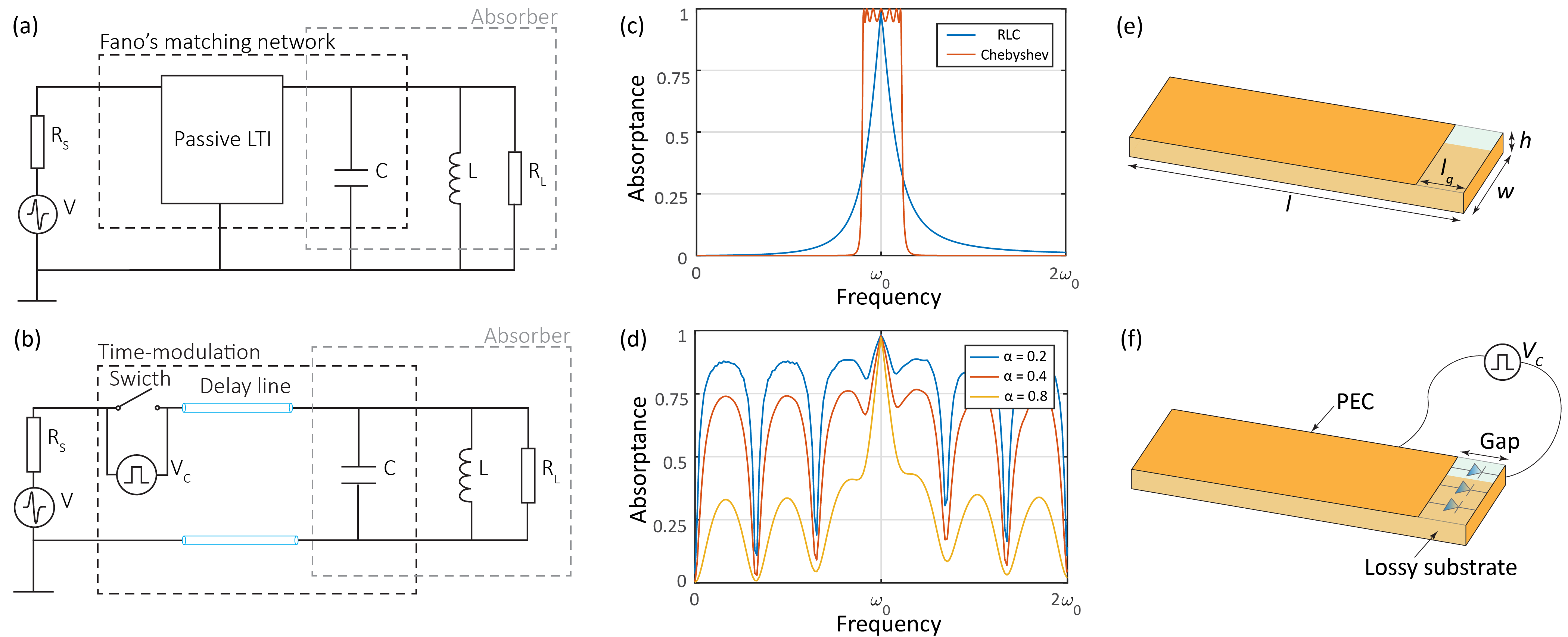
In this letter, we propose a practical approach to break the Bode-Fano limit of conventional absorbers by applying temporal modulation to integrated diodes/switches based on an energy trapping concept. The idea is to trap the incident ultra-wide band pulses within the resonator by adopting a modulated switch that cuts off the radiation path right after the signal fully enters the structure. As a proof of concept illustrated in Fig.1(b), the switch, along with a delay line with a delay time of , are inserted between the same Gaussian source and absorber as in Fig.(1)(a). The switch has a turn-on time of , synchronized with the pulse, and is then left off for the rest of the period, so that the input energy is allowed to only enter, but not to leave the network. As a result, the energy dissipates inside the network through multiple reflections. To obtain the transient response on , each reflection is treated separately using S parameters and summed up with its corresponding time shift (for details see Supplementary II).
| (2) |
| (3) |
| (4) |
where represents the transient response on the load during the reflection neglecting the time delay, is the input of the reflection, is the S parameters of parallel network, and is the original input from the broadband source. Here we define the imperfection of the switch by a leakage factor . If , all waves are trapped in the circuit. Otherwise part of the incoming energy leaks out due to the imperfection of the switch. Fig.1(d) shows the absorptance for a time-modulated absorber circuit model with different . Note that the absorptance across the whole spectrum is 1, assuming an ideal switch with is used. Even with a highly imperfect switch, a drastic increase of bandwidth is observed in Fig.1(d) compared with (c), breaking the Bode-Fano limits even when the upper limit of the Bode-Fano integral is chosen to be a finite value such as : as an example, for , .
The most straightforward way to realize the above circuit in an electromagetic structure is by adopting diode-integrated frequency selective surfaces (FSS) as the switch, and free space as the delay line (see Supplementary III). Thus, the ON and OFF states of the FSS corresponds to the ON and OFF states of the diodes. With the FSS in the OFF state, incident waves are allowed to propagate through; while in the ON state, the energy is trapped between the FSS and the conventional absorber. This method is rather general and can be applied to any passive absorber to broaden its bandwidth. However, the increased space needed conflicts with the objective of broadband absorption given a limited thickness. Thus, in this letter, a more practical low-profile PCB realization is shown in Fig.1(e) and (f). A horizontally propagating incident pulse/pulse train is coupled to the structure through the gap on the top surface, the length of the structure performs equivalently as the delay line in the circuit model, and the switch is replaced by step recovery diodes (SRD) contolled by a signal . Instead of a lumped resistor , the dissipation is distributive in the lossy FR4 substrate. When the control signal is low, the diodes are OFF, and energy couples into the absorber; when is high, the diodes turn ON, the absorber behaves as a closed cavity, and all the energy is trapped inside. The simulated static ON and OFF states results are included in Supplementary IV.
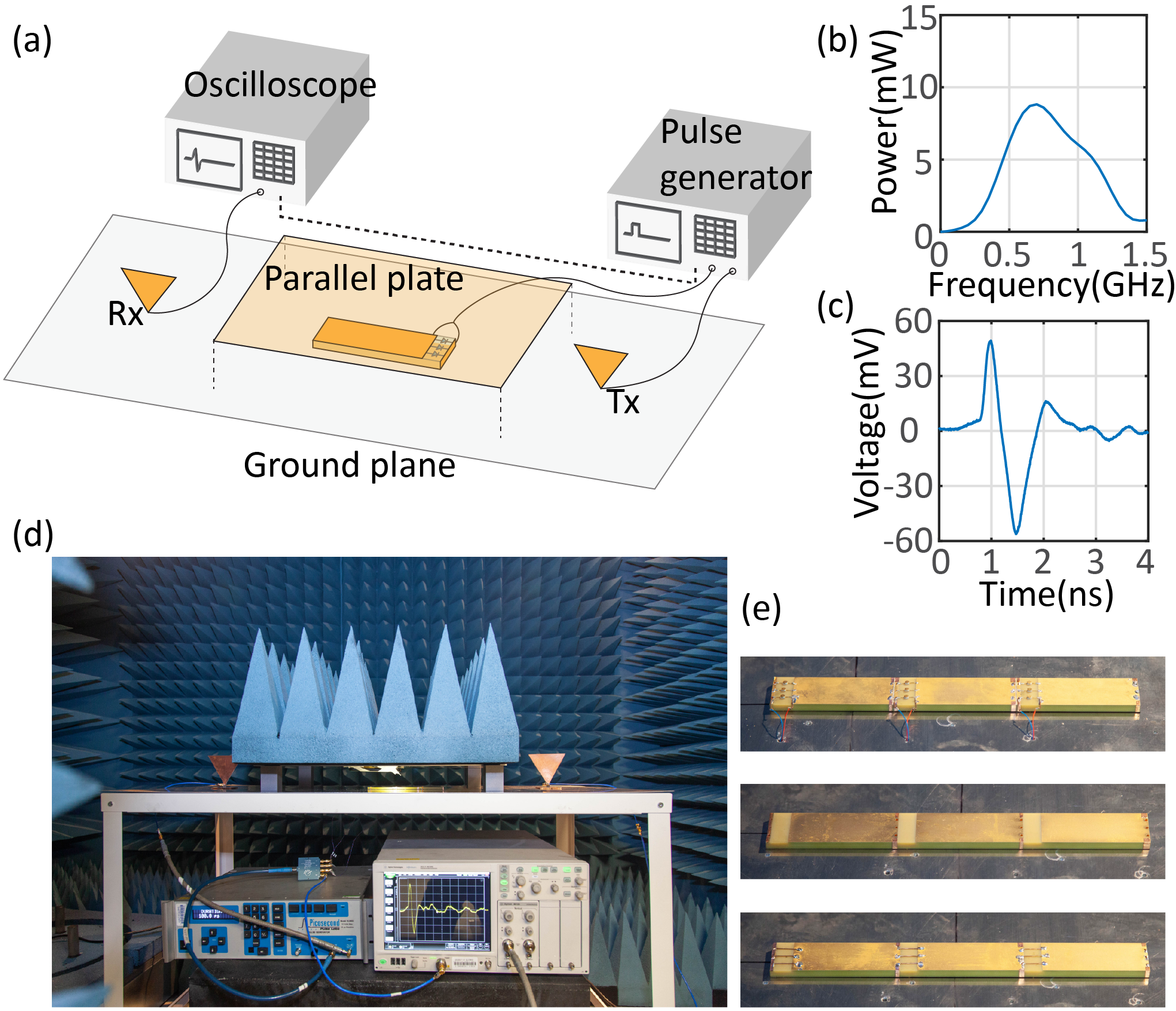
Measurement.— The measurement sample is shown in Fig.2. The size of the structure is the same as shown in Fig.1(e) and (f), and the measurement setup is illustrated in Fig.2(a). The non-modulated sample with static ON and OFF states, and the time-modulated sample are measured, respectively, for one, two and three units. The signal is generated by a fast rising pulse generator and radiated by a broadband monopole bow-tie antenna Tx sitting on a cm by cm ground plane, travelling through a parallel plate cm by cm by cm TEM waveguide (to confine energy) with the sample-under-test inside. The transmitted signal is received by another bow-tie antenna Rx and collected by a wide-band oscilloscope. The produced signal from the pulse generator is a V repetitive pulse train lasting ps with low duty cycle of and short rise time around ps. This signal is modulated by Tx forming a order derivative Gaussian-like pulse, collected by Rx. The spectrum and transient waveform is shown in Fig.2(b) and (c). The distance between Tx and Rx is cm. The osilloscope and the pulse generator are synchronized with the trigger signal of the latter, and part of the trigger signal is split out by a power divider to be used as the control signal for the time-modulated absorber. The trigger signal has an amplitude of around V and lasts for ns, which warrants adequate multi-reflection for sufficient dissipation. Short twisted wires with different lengths are adopted and tuned to precisely control the time delay between different units for multi-unit measurements when travelling wave modulation is performed. All the cables involved in this experiment are carefully chosen, such that the modulated signal synchronizes with the incident wave for the samples to trap as much energy as possible. For each configuration, the average of five sets of measurements is adopted to reduce noise and avoid fluctuations.
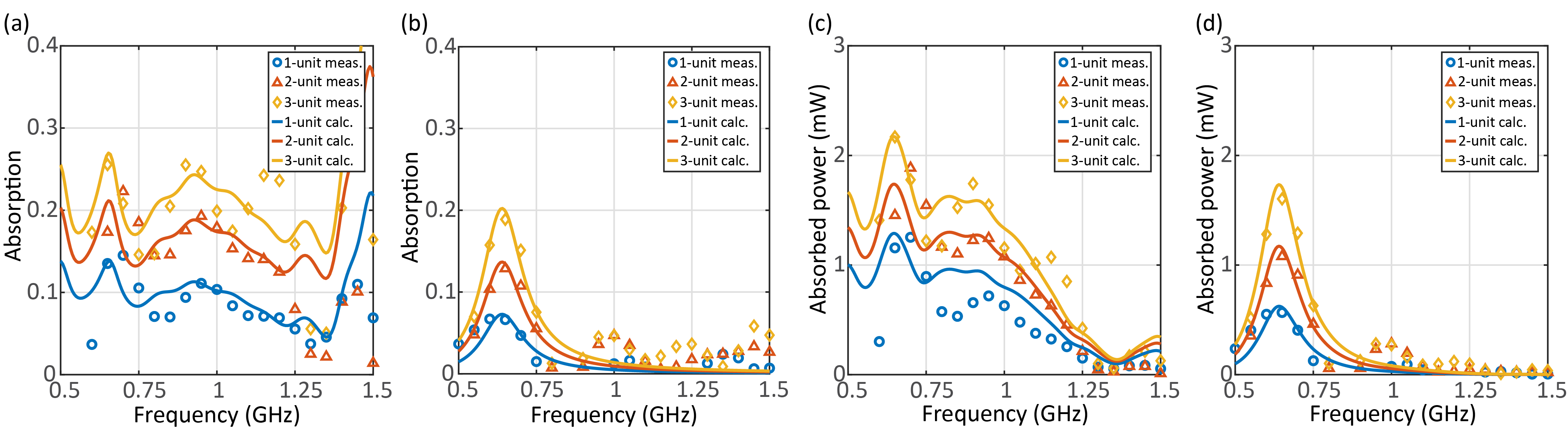
From an analytical perspective, the , , and required for S parameter calculation in (4) can be extracted from non-modulated measurement results in Fig.3(b) by
| (5) |
| (6) |
where MHz is the center frequency, MHz is the dB bandwidth. The resistance is chosen to be the characteristic impedance of free space Ohms.
Different from the circuit model in Fig.1(b), only a portion of radiation from Tx couples into the sample in the measurement. Therefore, a parameter is introduced to describe how much energy is captured by the units and Eq.(4) accordingly changes to
| (7) |
Moreover, since the loss is distributive, instead of evaluating the absorption by calculating the dissipation on , the absorptance and absorbed power is calculated with respect to transmission instead of absorption on the load by
| (8) |
| (9) |
in which,
| (10) |
corresponds to the transient transmission received by Rx and collected by the oscilloscope, and
| (11) |
For the measurement results, to exclude the disturbance of fields by the samples, the baseline is the ON state (replacing diodes with wires) instead of an empty waveguide.
| (12) |
| (13) |
where denotes transmitted signal measured with ON state, OFF state and time-modulated sample collected by the oscilloscope.
The measured and calculated absorptance is shown in Fig.3. As shown in Fig.3(b), the non-modulated sample absorbs energy at around the resonating frequency GHz, while the modulated sample has a broadband absorption starting from GHz to GHz. Due to difficulty in directly determining and through measurement, these two parameters are numerically fitted. It is found that when (indicating of the coupled energy leaks out when the diodes are ON) and for one-,two- and three-unit calculations, the predicted results show a good match with the measurement results in Fig.3. The calculated Bode-Fano integral and for modulated and non-modulated sample, respectively. The absorption increases as the number of units increases for both modulated and non-modulated cases, indicating the potential to accommodate this design to larger-scale metasurfaces.
Conclusion.— In this letter, we proposed an approach to break the Bode-Fano limit using time-modulation by creating an energy trap and discussed two possible EM structures based on the idea. Verified by analytical calculations, simulation results and measurement of the horizontal model, we proved the proposed method can achieve beyond the bandwidth limitations for passive LTI systems. The latter low-profile design integrates well with PCB and can be potentially applied to protect sensitive devices against broadband signals. Although measurements are done only for up to three units, the horizontal design could be extended to a metasurface. Further research may focus on self-triggering and self-delaying modules. Time-modulation also brings other interesting properties, such as non-reciprocity [32, 33, 34]. The horizontal model we propose also has non-reciprocal behaviour caused by the temporal modulation and is discussed in Supplementary IV.
The authors would like to acknowledge the support by Office of Naval Research under Grant No. N00014-20-1-2710.
References
- Pozar [2011] D. M. Pozar, Microwave engineering (John wiley & sons, 2011).
- Collin [2007] R. E. Collin, Foundations for microwave engineering (John Wiley & Sons, 2007).
- Balanis [1999] C. A. Balanis, Advanced engineering electromagnetics (John Wiley & Sons, 1999).
- Balanis [2015] C. A. Balanis, Antenna theory: analysis and design (John wiley & sons, 2015).
- Sedra et al. [1998] A. S. Sedra, D. E. A. S. Sedra, and K. C. Smith, Microelectronic circuits (New York: Oxford University Press, 1998).
- [6] C. Kopp, The e-bomb–a weapon of electrical mass destruction, in Proceedings of the InfoWarCon V Conference.
- Kopp [1996] C. Kopp, The electromagnetic bomb-a weapon of electrical mass destruction, Report (MONASH UNIV CLAYTON (AUSTRALIA), 1996).
- Cui et al. [2011] Y. Cui, J. Xu, K. Hung Fung, Y. Jin, A. Kumar, S. He, and N. X. Fang, A thin film broadband absorber based on multi-sized nanoantennas, Applied Physics Letters 99, 253101 (2011).
- Zhu et al. [2020] L. Zhu, Y. Jin, H. Liu, and Y. Liu, Ultra-broadband absorber based on metal-insulator-metal four-headed arrow nanostructure, Plasmonics 15, 2153 (2020).
- Yang and Shen [2007] J. Yang and Z. Shen, A thin and broadband absorber using double-square loops, IEEE Antennas and Wireless Propagation Letters 6, 388 (2007).
- Zhang et al. [2019] B. Zhang, C. Jin, and Z. Shen, Low-profile broadband absorber based on multimode resistor-embedded metallic strips, IEEE Transactions on Microwave Theory and Techniques 68, 835 (2019).
- Lei et al. [2018] L. Lei, S. Li, H. Huang, K. Tao, and P. Xu, Ultra-broadband absorber from visible to near-infrared using plasmonic metamaterial, Optics express 26, 5686 (2018).
- Liu et al. [2020] J. Liu, W. Chen, J.-C. Zheng, Y.-S. Chen, and C.-F. Yang, Wide-angle polarization-independent ultra-broadband absorber from visible to infrared, Nanomaterials 10, 27 (2020).
- Zhu et al. [2014] J. Zhu, Z. Ma, W. Sun, F. Ding, Q. He, L. Zhou, and Y. Ma, Ultra-broadband terahertz metamaterial absorber, Applied Physics Letters 105, 021102 (2014).
- Biabanifard et al. [2018] S. Biabanifard, M. Biabanifard, S. Asgari, S. Asadi, and C. Mustapha, Tunable ultra-wideband terahertz absorber based on graphene disks and ribbons, Optics Communications 427, 418 (2018).
- Chen et al. [2013a] X. Chen, H. Gong, S. Dai, D. Zhao, Y. Yang, Q. Li, and M. Qiu, Near-infrared broadband absorber with film-coupled multilayer nanorods, Optics letters 38, 2247 (2013a).
- Bode [1945] H. W. Bode, Network analysis and feedback amplifier design (Van Nostrand, 1945).
- Fano [1950] R. M. Fano, Theoretical limitations on the broadband matching of arbitrary impedances, Journal of the Franklin Institute 249, 57 (1950).
- Kerr [1995] A. Kerr, Some fundamental and practical limits on broadband matching to capacitive devices, and the implications for sis mixer design, IEEE transactions on microwave theory and techniques 43, 2 (1995).
- [20] A. Ghorbani, M. Ansarizadeh, N. McEwan, R. A. Abd-alhameed, and D. Zhou, The bode-fano integrals as an objective measure of antenna bandwidth reflection coefficient product limit, in 2006 International RF and Microwave Conference (IEEE) pp. 210–215.
- Ghorbani et al. [2006] A. Ghorbani, R. A. Abd-Alhameed, N. J. McEwan, and D. Zhou, An approach for calculating the limiting bandwidth-reflection coefficient product for microstrip patch antennas, IEEE transactions on antennas and propagation 54, 1328 (2006).
- Rozanov [2000] K. N. Rozanov, Ultimate thickness to bandwidth ratio of radar absorbers, IEEE Transactions on Antennas and Propagation 48, 1230 (2000).
- Shlivinski and Hadad [2018] A. Shlivinski and Y. Hadad, Beyond the bode-fano bound: Wideband impedance matching for short pulses using temporal switching of transmission-line parameters, Physical review letters 121, 204301 (2018).
- Sussman-Fort and Rudish [2009] S. E. Sussman-Fort and R. M. Rudish, Non-foster impedance matching of electrically-small antennas, IEEE Transactions on Antennas and Propagation 57, 2230 (2009).
- Chen et al. [2013b] P.-Y. Chen, C. Argyropoulos, and A. Alù, Broadening the cloaking bandwidth with non-foster metasurfaces, Physical review letters 111, 233001 (2013b).
- Shi et al. [2019] T. Shi, M.-C. Tang, Z. Wu, H.-X. Xu, and R. W. Ziolkowski, Improved signal-to-noise ratio, bandwidth-enhanced electrically small antenna augmented with internal non-foster elements, IEEE Transactions on Antennas and Propagation 67, 2763 (2019).
- Jing et al. [2014] H. C. Jing, X. J. Xu, and Y. E. Wang, Direct antenna modulation (dam) with switched patch antenna-performance analysis, Applied Computational Electromagnetics Society Journal 29 (2014).
- Yao and Wang [a] W. Yao and Y. E. Wang, An integrated antenna for pulse modulation and radiation, in Proceedings. 2004 IEEE Radio and Wireless Conference (IEEE Cat. No. 04TH8746) (IEEE) pp. 427–429.
- Yao and Wang [b] W. Yao and Y. Wang, Direct antenna modulation-a promise for ultra-wideband (uwb) transmitting, in 2004 IEEE MTT-S International Microwave Symposium Digest (IEEE Cat. No. 04CH37535), Vol. 2 (IEEE) pp. 1273–1276.
- Firestein et al. [2021] C. Firestein, A. Shlivinski, and Y. Hadad, Absorption and scattering by a temporally switched lossy layer: Going beyond the rozanov bound, arXiv preprint arXiv:2105.01487 (2021).
- Li and Alù [2021] H. Li and A. Alù, Temporal switching to extend the bandwidth of thin absorbers, Optica 8, 24 (2021).
- Correas-Serrano et al. [2015] D. Correas-Serrano, J. Gomez-Diaz, D. Sounas, Y. Hadad, A. Alvarez-Melcon, and A. Alù, Nonreciprocal graphene devices and antennas based on spatiotemporal modulation, IEEE Antennas and Wireless Propagation Letters 15, 1529 (2015).
- Li et al. [2020] A. Li, Y. Li, J. Long, E. Forati, Z. Du, and D. Sievenpiper, Time-moduated nonreciprocal metasurface absorber for surface waves, Optics Letters 45, 1212 (2020).
- Cardin et al. [2020] A. E. Cardin, S. R. Silva, S. R. Vardeny, W. J. Padilla, A. Saxena, A. J. Taylor, W. J. Kort-Kamp, H.-T. Chen, D. A. Dalvit, and A. K. Azad, Surface-wave-assisted nonreciprocity in spatio-temporally modulated metasurfaces, Nature communications 11, 1 (2020).