Thickness-induced crossover from strong to weak collective pinning
in exfoliated FeTe0.6Se0.4 thin films at 1 T
Abstract
We studied flux pinning in exfoliated FeTe0.6Se0.4 thin-film devices with a thickness from 30 to 150 nm by measuring the critical current density . In bulk FeTe0.6Se0.4, the flux pinning has been discussed in the framework of weak collective pinning, while there is little knowledge on the pinning mechanism in the thin-film region. From the thickness dependence of at a fixed magnetic field of 1 T, we found that the strong pinning is dominant below nm, while the weak collective pinning becomes more important above nm. This crossover thickness can be explained by the theoretical model proposed by van der Beek et al [Phys. Rev. B. 66, 024523 (2002)].
I Introduction
Since 2008, iron-based superconductors (IBSs) have been well studied as a new group of high-temperature superconductors because of the two-dimensional layered structure similar to cuprate superconductors [1]. Their fundamental properties such as the short coherence length and large upper-critical field are useful for superconducting wires [2]. For such applications, it is essential to increase the critical current density . In order to achieve this, the pinning mechanism of magnetic vortices needs to be clarified.
Among all kinds of IBSs, the iron-based chalcogenide FeTe1-xSex with (FTS) has the simplest crystal structure with only Fe ( Se or Te) layers. There have been many reports on bulk [3, 4, 5, 6, 7, 8, 9, 10, 11, 12] and thin-film [13, 14, 15, 16] FTS single crystals, which enable a detailed discussion of the pinning mechanism. Although the critical temperature is not so high, the upper critical field is comparable to other IBSs. Thus, FTS has a potential to replace low-temperature superconducting wires such as Nb-Ti superconductors. In addition, FTS is a candidate for topological superconductor. Particularly it has been intensively studied on the detection of zero energy vortex bound state (ZVBS) in magnetic vortices, which is a fingerprint of the Majorana quasiparticles [17, 18, 19, 20]. In fact, a recent scanning tunneling microscopy study demonstrated the existence of ZVBS in magnetic vortices [19]. Simultaneously, however, it also revealed that some of the magnetic vortices do not contain the ZVBS. This suggests that the Majorana zero modes gain finite energies via the interaction between magnetic vortices, resulting in an energy splitting of the zero modes. In order to unveil the ZVBS in the superconducing FTS, it is helpful to understand the magnetic vortex lattice and also its pinning mechanism under finite magnetic fields.
In general, there are two pinning mechanisms in superconductors, i.e., weak collective pinning [21, 22] and strong pinning [23, 24]. In the former case, the pinning stems from the atomic-scale inhomogeneity of the superconducting regions due to impurities or defects and is further categorized into two types. One is pinning, originating from spatial fluctuations of the mean free path due to lattice defects [21]. This is related to the derivative of the macroscopic wave function in the Ginzburg-Landau theory. The other is pinning, originating from spatial fluctuations of the critical temperature [21]. This is related to the fact that the coefficient of the probability density for the macroscopic wave function in the Ginzburg-Landau theory is proportional to . For FTS single crystals, the pinning mechanisms have been determined by analyzing magnetization measurements with the Bean model [4, 5, 6, 7, 8]. In most cases the pinning is dominant [4, 5, 6], while in some cases both the and pinnings coexist [7, 8].
Contrary to the weak collective pinning, the strong pinning takes place at large-sized defects comparable to the coherence length ( nm) and can induce a high critical current density [25, 26]. It has been established that the strong pinning is a dominant mechanism for 100–300 nm thick YBa2Cu3O7-x (YBCO) films where the critical current density has a large value [24, 27]. Although there are some reports on enhanced critical current densities [28, 29, 30] as well as strong pinning [31, 32, 33] in IBS thin films, the relation between the strong pinning and the thickness of IBSs has not been fully elucidated yet.
In this work, we directly obtained in exfoliated FeTe0.6Se0.4 thin-film devices with several different thicknesses by measuring current-voltage properties at a fixed out-of-plane magnetic field of 1 T. For nm, linearly increases with increasing . Such a tendency is consistent with the strong pinning reported in YBCO thin-film superconductors. When exceeds nm, decreases with increasing and eventually approaches the value estimated for bulk FTS. By plotting as a function of , we observe a crossover behavior from the strong pinning in thin-film regions to the weak collective pinning. This crossover thickness nm can be explained by the theoretical model proposed by van der Beek et al [24].
II Experimental details
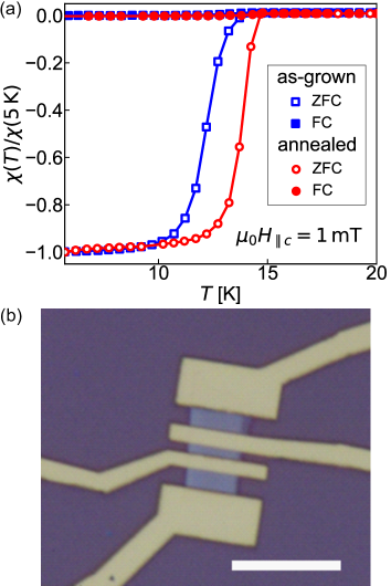
Single crystals of FeTe0.6Se0.4 were grown from a stoichiometric mixture of Fe, Te, and Se powder. We note that in the present work, FeTe0.6Se0.4 has been studied, but we use the same abbreviation (FTS) as for a general composition ratio FeTe1-xSex in this paper. The mixture was loaded into an alumina crucible and sealed in an evacuated quartz tube. The quartz tube was heated at 650∘C for 10 h and then 1070∘C for 15 h, followed by cooling down to 620∘C at a rate of 3∘C/h. FTS has a van-der-Waals interaction between the two adjacent Ch layers, which makes it easier to fabricate thin-film devices using the mechanical exfoliation technique. On the other hand, it has been known that excess Fe is present in between the Ch layers, which gives rise to magnetic correlations and suppresses the superconductivity [34]. To remove the excess Fe, we annealed as-grown FTS bulk crystals at 400∘C for 40 h under 1% atmosphere of O2 gas [35, 36, 37]. To determine of FTS bulk crystals, we measured the magnetic susceptibility using Magnetic Property Measurement System (Quantum Design). Figure 1(a) shows the temperature dependence of the magnetic susceptibility for as-grown and annealed FTS. In this work, is defined as a temperature where for zero-field cooling (ZFC) starts to decrease. From the measurements, we determine K for the as-grown sample and K for the annealed crystal. By annealing the FTS crystal, has been enhanced by 5%, which is consistent with Refs. [35, 36, 37]. Hereafter, we mainly focus on the annealed FTS unless otherwise noted, whereas we also use the as-grown FTS for comparison.
To obtain thin-film devices, we adopted the mechanical exfoliation technique using Scotch tapes under ambient conditions. Some of the exfoliated FTS flakes onto the Scotch tape were transferred to a thermally oxidized silicon substrate. We then coated polymethyl-methacrylate resist on the substrate and patterned electrodes with electron beam lithography. After the development of the resist, Ti (5 nm) and Au (150 nm) were deposited. Ti works as an adhesion layer for the Si/SiO2 substrate. Before the deposition of electrodes, we performed Ar milling process for 55 s to remove the residual resist at the surface of FTS. In fact, we have confirmed the following: (1) This process does not give significant damage to FTS; (2) without the Ar milling process, we cannot obtain an Ohmic contact between FTS and the electrodes because of the residual resist at the interface. Figure 1(b) shows an optical microscope image of a typical device. The thickness of FTS was determined with a commercially available atomic force microscopy after finishing transport measurements. Although we sometimes found not-perfectly homogeneous thin-film flakes, we regarded as a film thickness when surface regions with exceeds 85%. In the present work, ranges from 30 to 150 nm. Because of the limitation of the present exfoliation method, we could not obtain FTS devices thicker than 150 nm. We measured the resistivity of thin-film FTS devices with a standard Lock-in technique. To determine , we performed current ()-voltage () measurements.
III experimental results
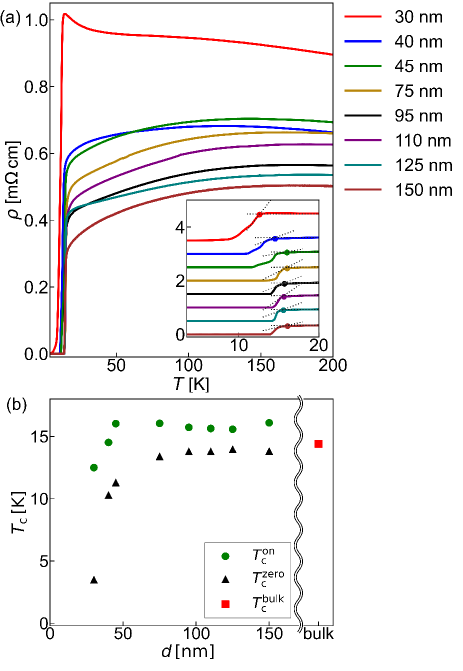
First, to determine of FTS thin-film devices, we measured the temperature dependence of the resistivity in Fig. 2(a). When the film thickness is larger than 100 nm, decreases with decreasing for the whole temperature region. Below nm, on the other hand, slightly increases with decreasing , takes a maximum and becomes zero at low temperatures. In particular, a 30 nm thick device shows insulating behavior down to 13 K. Such tendencies are due to the inhomogeneity of superconducting states in FTS crystals, as reported in Ref. [38]. The superconducting percolation network, which is strongly connected in bulk, gradually weakens with decreasing . This results in weak superconductivity for thinner FTS film devices. Figure 2(b) shows the thickness dependence of . There are two ways to define : One is to use the initial rise of resistivity from zero (), and the other is to use the onset of resistivity drop in - curve () as indicated in Fig. 2(a). Since there is a finite voltage jump even just below [see Fig. 3(a)], in this work we have adopted as , namely, . starts to decrease below nm and should vanish at nm. According to Ref. [36], the critical thickness below which vanishes is 12 nm, which is consistent with the present work.
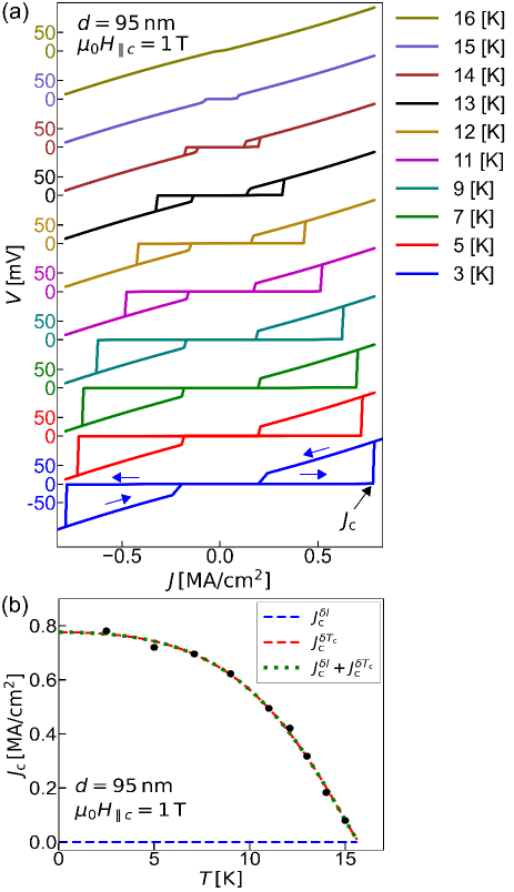
Next we performed - measurements under the out-of-plane magnetic field T. Figure 3(a) shows current-voltage curves for a 95 nm thick FTS device at several different temperatures. We use the current density instead of to compare with different devices. At low temperatures, there is a clear hysteresis that originates from the Joule heating in the FTS device. In the present work, we define as the current density when the measured voltage exceeds a threshold value of 1 mV. For example, is 0.78 MA/cm2 at K. In the vicinity of , on the other hand, the hysteresis vanishes and the voltage jump near becomes less clear. We also performed pulse current measurements with a pulse width of 1 ms and an interval of 100 ms in order to evaluate without the effects of Joule heating. The obtained was almost the same value as in Fig. 3(a). In Fig. 3(b), obtained from Fig. 3(a) is plotted as a function of . monotonically decreases with increasing and vanishes at .
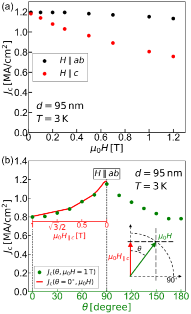
We also measured the magnetic field and angle dependences of for the nm thick FTS device at K. Figure 4(a) shows as a function of along the axis and the plane. When the magnetic field is applied along the plane, is more or less constant. For the perpendicular magnetic field , on the other hand, decreases with increasing . Figure 4(b) shows at T as a function of the rotation angle from the axis. has a broad maximum at , and there is no peak at nor . If we assume that depends only on the axis component of the applied magnetic field, i.e., , the angle dependence of is expected as shown by the red curve, which is consistent with the experimental data. This clearly shows that depends only on the perpendicular component of the magnetic field. Such magnetic field and angle dependences of are consistent with previous works on FTS thin films [13, 14, 15, 16].
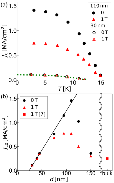
Now we move on to the dependence of . In Fig. 5(a), we show the temperature dependence of measured at T and 1 T for and 110 nm thick devices, respectively. There is almost no difference in between 0 and 1 T for the 30 nm thick device, whereas the difference is significant for the 110 nm thick device. To see the dependence of at 0 and 1 T more systematically, we plot , which is obtained by extrapolating the vs curves down to as detailed in the next section at and 1 T. linearly increases with up to nm for 1 T and nm for 0 T. Above nm, suddenly decreases with increasing and approaches a value evaluated with the Bean model [7]. Figure 5(b) clearly indicates that there are two regions below nm and above nm; the former is the strong pinning region and the latter is the weak collective pinning region, as discussed in more detail in the next section.
IV discussions
IV.1 Strong pinning
We first discuss the strong pinning region below nm. It is known that FTS is a highly inhomogeneous material [39, 40, 41, 42, 19]. According to electron energy loss spectroscopy measurements [42], there is an inhomogeneous distribution of Te in FTS crystals; it forms some clusters in FTS and the spatial variation of the cluster is approximately 10 nm. Therefore, the effect of the inhomogeneity should be prominent when is of the order of 10 nm, where the strong pinning is more dominant [24, 27].
Lower magnetic fields are favorable to confirm whether the strong pinning is essential in our thin-film FTS devices. This is because the vortex density in the low field region is too small for weak collective pinning to contribute and only the strong pinning contributes to [43]. Therefore, we measured at T (but probably with a small Oersted field). Then , at , was obtained by fitting vs curves with some theoretical model. We first tried theoretical expressions discussed in Ref. [24] for the strong pinning, but none of them could reproduce our experimental data. Thus we adopted Eqs. (2)–(4) to fit the vs curves. We note that Eqs. (2)–(4) are originally developed for the weak collective pinning region, as detailed in the next subsection. As shown in Fig. 5(a), for the nm thick device can be fitted with Eqs. (2)–(4). The evaluated does not depend on the applied magnetic field at least within 1 T and linearly increases with increasing . In fact, these features cannot be explained by the weak collective theory but are consistent with the strong pinning theory, as detailed below. This fact also suggests that Eqs. (2)–(4) would be useful even for the strong pinning.
As mentioned above, at 0 T has the same value as at 1 T and linearly increases with up to nm [see Fig. 5(b)]. Such a dependence of has also been observed in YBCO films [44, 24, 27, 45, 46]. According to a theoretical model proposed by van der Beek et al. [24], the critical current density for very thin superconducting films is given by
| (1) |
where is the typical energy scale for single vortex, is the flux quantum, is the in-plane magnetic penetration depth at , H/m, is the in-plane coherence length at , and is the critical thickness where becomes zero. and are the typical sizes of defect along the plane and axis, respectively; is the crossover film thickness from the very thin-film region to relatively thick film region [24]. As described by Eq. (1), in the very thin-film region should be field-independent and linearly increases with increasing . This is consistent with the dependence of for nm in Fig. 5(b), at least in the field range from 0 to 1 T. Furthermore, is also consistent with the thickness below which vanishes in Fig. 2(b). The contribution of the strong pinning is more significant in this thickness range.
As we increase further from 70 nm, a significant difference in is observed between and 1 T. takes a maximum value at nm for both magnetic fields and suddenly decreases with increasing . This thickness range will be discussed in the next subsection. From the linear fitting for below nm, we obtain the slope . By using nm [13], m [34] and assuming nm, we estimate the crossover film thickness to be nm. This value is consistent with the experimental crossover thickness ( nm) shown in Fig. 5(b).
IV.2 Weak collective pinning
It has been established that in bulk FTS can be described by the weak collective pinning theory [21]. As shown in Fig. 5(b), at 1 T in bulk FTS is very close to that in our thin-film devices with nm. Therefore, we analyze using the weak collective pinning theory, as discussed for bulk FTS in previous works [4, 5, 6, 7, 8]. In the theoretical approach proposed by Griessen et al. [22], in the moderately low field region, where the strong pinning can be ignored and the motion of single vortex is essential, is given as
| (2) |
for pinning and
| (3) |
for pinning; is the reduced temperature (). and are values at absolute zero temperature for pinning and pinning, respectively. If both pinning mechanisms coexist, can be written as:
| (4) |
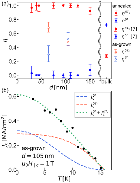
In Fig. 3(b), we show the best fit with Eqs. (2)–(4) for the 95 nm thick FTS device. We use two fitting parameters ( and ) and obtain MA/cm2, MA/cm2, respectively. It is obvious that is much larger than , indicating that the pinning is much more dominant. In Fig. 6(a), we show the thickness dependence of and obtained from fitting, where is the total critical current density at . As mentioned in the previous subsection, the fitting with Eqs. (2)–(4) works even for the strong pinning region. In the present range, is much larger than , indicating that the pinning is more dominant. With increasing , the proportion of becomes larger and exceeds that of [7] in bulk FTS. This fact suggests that a crossover from the strong pinning to the weak collective pinning occurs at nm.
Let us discuss the reason why the pinning is dominant in our thin-film devices. One possibility is the existence of excess Fe atoms. In most previous works on bulk FTS [4, 5, 6] where as-grown samples were used, the pinning is dominant. In such a case, a small amount of Fe impurities would be in between the two chalcogen layers. To remove the Fe impurities, Sun et al. performed oxygen annealing for FTS and found that both the and the pinnings coexist [7]. As mentioned in Sec. II, excess Fe (i.e., atomic-scale) impurities would be segregated at the surface of FTS by annealing it under an oxygen flow. This results in the reduction of the pinning contribution. To confirm the above scenario, we fabricated as-grown FTS thin-film devices and measured the temperature dependence of the critical current density in the same way as for annealed FTS devices. Figure 6(b) shows the temperature dependence of for a 105 nm thick as-grown FTS device and also the result of fitting with Eqs. (2)–(4). When we measured - curves for as-grown devices, the critical current changed with every measurement. Therefore, the data points in Fig. 6(b) are scattered compared with those for the annealed FTS device shown in Fig. 3(b). From the fitting with Eqs. (2)–(4), and can be evaluated, as indicated by the triangle points in Fig. 6(a). The contribution of pinning is comparable to that of pinning, even at nm where the latter is much more dominant than the former in the annealed devices. This clearly shows that the excess Fe plays an important role in the pinning mechanism in FTS. We note that even in as-grown FTS thin-film devices, the contribution of pinning is larger than that of the annealed bulk FTS sample.
Another possibility is the similarity between pinning and strong pinning. In the case of strong pinning at nanometer-sized defects, the pinning is less important than the pinning, as pointed out in Ref. [24]. This is because the scattering cross section of quasiparticles at atomic-scale defects is negligibly small compared with that at large-sized defects. In thin-film FTS devices [42], the inhomogeneous distribution of Te would be more essential. Therefore, the contribution of the pinning is much more dominant in annealed FTS thin-film devices and is still large even in as-grown FTS thin-film devices which contain many atomic-scale defects. In bulk FTS, on the other hand, quasiparticles may scatter at atomic-scale defects and thus the pinning can be dominant because the path of the superconducting state is robust and the inhomogeneous distribution is not crucial [38].
V Conclusion
We have studied the critical current density in FeTe0.6Se0.4 (FTS) devices with thicknesses from 30 to 150 nm by means of electric transport measurements. Below nm, does not depend on the applied magnetic field and linearly increases with increasing . This result is consistent with the strong pinning theory. Above nm, on the other hand, decreases with increasing and becomes comparable to that for bulk FTS, suggesting that the thicker film region corresponds to the weak collective pinning region. From these experimental results, a crossover from the strong pinning to the weak collective pinning is realized at nm at a fixed magnetic field of 1 T. This value can be explained by the theoretical model where a defect size is comparable to the inhomogeneity of Te ( nm) in FTS. Moreover, the pinning is much more dominant than the pinning in our thin-film devices. This is partly due to the fact that our FTS have been annealed under an oxygen flow before the exfoliation, resulting in a reduction of excess Fe (i.e., atomic-size impurities) in between the two chalcogen layers.
Acknowledgements.
This work was supported by JSPS KAKENHI (Grants No. JP16H05964, No. JP17K18756, No. JP19K21850, No. JP19H00656, No. JP19H05826, No. JP20H02557, No. JP20J20229, and No. JP21J20477), the Mazda Foundation, the Shimadzu Science Foundation, the Yazaki Memorial Foundation for Science and Technology, the SCAT Foundation, the Murata Science Foundation, Toyota Riken Scholar, the Kato Foundationfor Promotion of Science, and the Asahi Glass foundation.References
- [1] Y. Kamihara, T. Watanabe, M. Hirano, and H. Hosono, J. Am. Chem. Soc. 130, 3296 (2008).
- [2] H. Hosono, A. Yamamoto, H. Hiramatsu, and Y. Ma, Mater. Today 21, 278 (2018).
- [3] B. C. Sales, A. S. Sefat, M. A. McGuire, R. Y. Jin, D. Mandrus, and Y. Mozharivskyj, Phys. Rev. B 79, 094521 (2009).
- [4] P. Das, A. D. Thakur, A. K. Yadav, C. V. Tomy, M. R.Lees, G. Balakrishnan, S. Ramakrishnan, and A. K. Grover, Phys. Rev. B 84, 214526 (2011).
- [5] M. Bonura, E. Giannini, R. Viennois, and C. Senatore,Phys. Rev. B 85, 134532 (2012).
- [6] A. Galluzzi, K. Buchkov, V. Tomov, E. Nazarova, A. Leo,G. Grimaldi, S. Pace, and M. Polichetti, Supercond. Sci. Technol. 33, 094006 (2020).
- [7] Y. Sun, T. Taen, Y. Tsuchiya, S. Pyon, Z. Shi, and T.Tamegai, Europhys. Lett. 103, 57013 (2013).
- [8] T. Tamegai, Y. Sun, T. Yamada, and S. Pyon, IEEETransactions on Applied Superconductivity 26, 1 (2016).
- [9] C. Yadav and P. Paulose, Solid State Commun. 151, 216 (2011).
- [10] D. Miu, T. Noji, T. Adachi, Y. Koike, and L. Miu, Supercond. Sci. Technol. 25, 115009 (2012).
- [11] M. Shahbazi, X. L. Wang, S. X. Dou, H. Fang, and C. T.Lin, J. Appl. Phys. 113, 17E115 (2013).
- [12] Z. F. Wu, Z. H. Wang, J. Tao, L. Qiu, S. G. Yang, and H. H. Wen, Supercond. Sci. Technol. 29, 035006 (2016).
- [13] K. Iida, J. Hänisch, E. Reich, F. Kurth, R. Hühne, L. Schultz, B. Holzapfel, A. Ichinose, M. Hanawa, I. Tsukada, M. Schulze, S. Aswartham, S. Wurmehl, and B. Büchner, Phys. Rev. B 87, 104510 (2013).
- [14] V. Braccini, S. Kawale, E. Reich, E. Bellingeri, L. Pellegrino, A. Sala, M. Putti, K. Higashikawa, T. Kiss, B. Holzapfel, and C. Ferdeghini, Appl. Phys. Lett. 103, 172601 (2013).
- [15] P. Yuan, Z. Xu, Y. Ma, Y. Sun, and T. Tamegai, Supercond. Sci. Technol. 29, 035013 (2016).
- [16] H. Bryja, R. Hühne, K. Iida, S. Molatta, A. Sala, M.Putti, L. Schultz, K. Nielsch, and J. H änisch, Supercond. Sci. Technol. 30, 115008 (2017).
- [17] P. Zhang, K. Yaji, T. Hashimoto, Y. Ota, T. Kondo, K. Okazaki, Z. Wang, J. Wen, G. D. Gu, H. Ding, and S. Shin, Science 360, 182 (2018).
- [18] D. Wang, L. Kong, P. Fan, H. Chen, S. Zhu, W. Liu, L. Cao, Y. Sun, S. Du, J. Schneeloch, R. Zhong, G. Gu, L.Fu, H. Ding, and H. J. Gao, Science 362, 333 (2018).
- [19] T. Machida, Y. Sun, S. Pyon, S. Takeda, Y. Kohsaka, T.Hanaguri, T. Sasagawa, and T. Tamegai, Nat. Mater. 18, 811 (2019).
- [20] S. Zhu, L. Kong, L. Cao, H. Chen, M. Papaj, S. Du, Y. Xing, W. Liu, D. Wang, C. Shen, F. Yang, J. Schneeloch, R. Zhong, G. Gu, L. Fu, Y. Y. Zhang, H. Ding, and H. J. Gao, Science 367, 189 (2020).
- [21] G. Blatter, M. V. Feigel’man, V. B. Geshkenbein, A. I. Larkin, and V. M. Vinokur, Rev. Mod. Phys. 66, 1125 (1994).
- [22] R. Griessen, W. Haihu, A. J. J. van Dalen, B. Dam, J. Rector, H. G. Schnack, S. Libbrecht, E. Osquiguil, and Y. Bruynseraede, Phys. Rev. Lett. 72, 1910 (1994).
- [23] Y. N. Ovchinnikov and B. I. Ivlev, Phys. Rev. B 43, 8024 (1991).
- [24] C. J. van der Beek, M. Konczykowski, A. Abal’oshev, I. Abal’osheva, P. Gierlowski, S. J. Lewandowski, M. V. Indenbom, and S. Barbanera, Phys. Rev. B. 66, 024523 (2002).
- [25] W. K. Yeoh, J. Horvat, S. X. Dou, and V. Keast, Supercond. Sci. Technol. 17, S572 (2004).
- [26] Z. Chen, F. Kametani, Y. Chen, Y. Xie, V. Selvamanickam, and D. C. Larbalestier, Supercond. Sci. Technol. 22, 55013 (2009).
- [27] A. O. Ijaduola, J. R. Thompson, R. Feenstra, D. K. Christen, A. A. Gapud, and X. Song, Phys. Rev. B. 73, 134502 (2006).
- [28] P. Mele, K. Matsumoto, K. Fujita, Y. Yoshida, T. Kiss, A. Ichinose, and M. Mukaida, Supercond. Sci. Technol. 25, 84021 (2012).
- [29] W. Si, S. J. Han, X. Shi, S. N. Ehrlich, J. Jaroszynski, A. Goyal, and Q. Li, Nat. Commun. 4, 1347 (2013).
- [30] J. Lee, J. Jiang, F. Kametani, M. J. Oh, J. D. Weiss, Y. Collantes, S. Seo, S. Yoon, C. Tarantini, Y. J. Jo, E. E. Hellstrom, and S. Lee, Supercond. Sci. Technol. 30, 85006 (2017).
- [31] K. Iida, J. Hänisch, S. Trommler, V. Matias, S. Haindl, F. Kurth, I. L. del Pozo, R. Hühne, M. Kidszun, J. Engelmann, L. Schultz, and B. Holzapfel, Appl. Phys. Express 4, 013103 (2010).
- [32] Y. Zhang, C. T. Nelson, S. Lee, J. Jiang, C. W. Bark, J. D. Weiss, C. Tarantini, C. M. Folkman, S.-H. Baek, E. E. Hellstrom, D. C. Larbalestier, C.-B. Eom, and X. Pan, Appl. Phys. Lett. 98, 042509 (2011).
- [33] E. Bellingeri, S. Kawale, I. Pallecchi, A. Gerbi, R. Buzio, V. Braccini, A. Palenzona, M. Putti, M. Adamo, E. Sarnelli, and C. Ferdeghini, Appl. Phys. Lett. 100, 082601 (2012).
- [34] M. Bendele, S. Weyeneth, R. Puzniak, A. Maisuradze, E. Pomjakushina, K. Conder, V. Pomjakushin, H. Luetkens, S. Katrych, A. Wisniewski, R. Khasanov, and H. Keller, Phys. Rev. B 81, 224520 (2010).
- [35] Y Sun, T Taen, Y Tsuchiya, Z X Shi, and T Tamegai, Supercond. Sci. Technol. 26, 015015 (2013).
- [36] Y. Sun, Y. Tsuchiya, T. Taen, T. Yamada, S. Pyon, A.Sugimoto, T. Ekino, Z. Shi, and T. Tamegai, Sci. Rep. 4, 4585 (2014).
- [37] Y. Sun, Z. Shi, and T. Tamegai, Supercond. Sci. Technol. 32, 103001 (2019).
- [38] C. Yue, J. Hu, X. Liu, A. M. Sanchez, Z. Mao, and J. Wei, ACS Nano 10, 429 (2016).
- [39] B. Joseph, A. Iadecola, A. Puri, L. Simonelli, Y. Mizuguchi, Y. Takano, and N. L. Saini, Phys. Rev. B 82, 20502(R) (2010).
- [40] H. Hu, J.-M. Zuo, J. Wen, Z. Xu, Z. Lin, Q. Li, G. Gu, W. K. Park, and L. H. Greene, New J. Phys. 13, 53031 (2011).
- [41] U. R. Singh, S. C. White, S. Schmaus, V. Tsurkan, A. Loidl, J. Deisenhofer, and P. Wahl, Phys. Rev. B 88, 155124 (2013).
- [42] Y. Zhu, L. Chen, J. Ciston, and H. Wang, J. Phys. Chem. C 117, 7170 (2013).
- [43] C. J. van der Beek, G. Rizza, M. Konczykowski, P. Fertey, I. Monnet, T. Klein, R. Okazaki, M. Ishikado, H. Kito, A. Iyo, H. Eisaki, S. Shamoto, M. E. Tillman, S. L. Bud’ko, P. C. Canfield, T. Shibauchi, and Y. Matsuda, Phys. Rev. B 81, 174517 (2010).
- [44] E. Sheriff, R. Prozorov, Y. Yeshurun, A. Shaulov, G. Koren, and C. Chabaud-Villard, J. Appl. Phys. 82, 4417 (1997).
- [45] X. Wang and J. Z. Wu, Phys. Rev. B. 76, 184508 (2007).
- [46] Y. V. Cherpak, V. L. Svetchnikov, A. V. Semenov, V. O. Moskaliuk, C. G. Tretiatchenko, V. S. Flis, and V. M. Pan, J. Phys.: Conf. Ser. 97, 012259 (2008).