Non-reciprocal Pauli Spin Blockade in a Silicon Double Quantum Dot
Abstract
Spin qubits in gate-defined silicon quantum dots are receiving increased attention thanks to their potential for large-scale quantum computing. Readout of such spin qubits is done most accurately and scalably via Pauli spin blockade (PSB), however various mechanisms may lift PSB and complicate readout. In this work, we present an experimental observation of a new, highly prevalent PSB-lifting mechanism in a silicon double quantum dot due to incoherent tunneling between different spin manifolds. Through dispersively-detected magnetospectroscopy of the double quantum dot in 16 charge configurations, we find the mechanism to be energy-level selective and non-reciprocal for neighbouring charge configurations. Additionally, using input-output theory we report a large coupling of different electron spin manifolds of 7.90 , the largest reported to date, indicating an enhanced spin-orbit coupling which may enable all-electrical qubit control.
I Introduction
Spin qubits in gate-defined silicon quantum dots (QDs) have emerged as a promising platform for implementing large-scale quantum computation owing to their long coherence times, compact size and ability to be operated at relatively high temperatures of 1-5 K [1, 2, 3, 4, 5, 6]. Moreover, silicon spin qubits can be fabricated using industrial semiconductor manufacturing techniques, thereby presenting a path to high-yield large-scale device fabrication in which control electronics may also be integrated on-chip [7, 8, 9, 10, 11]. With the increasing emphasis on scalability, it is becoming increasingly attractive to pursue methods of spin qubit control and readout that avoid additional on-chip components, complex device architectures, and operational constraints such as vicinity to charge reservoirs [12, 13, 14, 15, 16, 17, 18].
Readout of silicon spin qubits is achieved by spin-to-charge conversion, a process that translates the spin degree of freedom to a selective movement of charge and that is typically performed via Pauli spin blockade (PSB) between two QDs or spin-selective tunneling to a reservoir [19, 20]. In both cases, the movement of charge can be measured using charge sensors, such as a single-electron transistor or single-electron box [21, 22, 23], but only PSB can be detected dispersively using resonant circuits thus alleviating the need for electrometers and reservoirs adjacent to the qubit [24, 25]. Moreover, PSB has been shown to provide high-fidelity readout, even at low magnetic fields and elevated temperatures [26, 5, 27, 28].
Pauli spin blockade, however, may be lifted thus compromising readout. Lifting of PSB may occur due to direct tunneling between triplets [24] or due to fast tunneling to low-energy high-spin states, such as the four-electron quintet, which may result from small valley-orbit splittings and generally dense QD energy spectra [29, 30, 31]. Additionally, theory predicts that fast relaxation processes happening at rates similar or faster than the readout probe frequency can lift dispersively-detected PSB [32], and work on a charge-sensed GaAs double quantum dot (DQD) has observed spin blockade lifting due to dephasing arising from hyperfine and spin-orbit interactions [33].
In this Letter, we investigate the spin-blockade physics of a dispersively-sensed CMOS silicon DQD in 16 charge configurations and demonstrate non-reciprocal and energy-level-selective presence of PSB. We show that PSB lifting is highly prevalent and occurs due to fast decoherence, thus expanding the understanding of dispersively-detected PSB in silicon and providing a path to positive detection of different spin manifolds by selection of the readout detuning point. By analysis of the response of a resonator coupled to the DQD using input-output theory, we determine a coupling between different electron spin manifolds of 7.90 , the largest reported to date. Our results indicate the presence of enhanced spin-orbit coupling (SOC) and motivate electrical spin manipulation experiments via electric-dipole spin resonance (EDSR).
II Non-reciprocal Pauli spin blockade
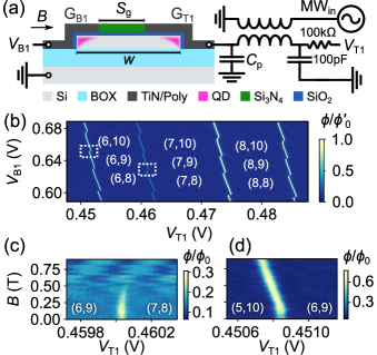
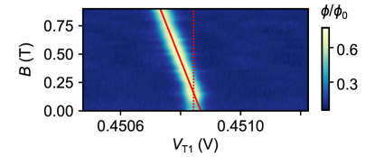
Figure 1(a) shows the split-gate nanowire field-effect transistor used in this work. To facilitate gate-based sensing [34], gate , which we note overlaps the channel nm more than , is wirebonded to a superconducting NbN spiral inductor on a separate chip, thus forming a resonant circuit with resonance frequency GHz at zero magnetic field . For further details about the transistor, inductor, and setup, see Appendix A and Ref. [35]. A DQD constituted by a pair of low-symmetry QDs is formed in the upper corners of the nanowire channel when positive dc biases applied to and attract electrons from the source and drain reservoirs. The number of electrons accumulated in the DQD is governed by the gate voltages and and changes in the DQD electron occupancy are detected dispersively by probing the resonator via the transmission line with a frequency close to and monitoring the phase shift of the reflected signal . Non-zero phase shifts occur as a result of cyclical interdot or dot-to-reservoir tunneling events happening under the influence of the microwave probe resulting in a finite DQD-resonator coherent coupling rate [32, 35]. Figure 1(b), which plots the phase shift relative to the largest dot-reservoir transition phase shift in the measured region, , as a function of and , shows the honeycomb pattern characteristic of a DQD charge stability diagram. The electron occupancies indicated in Fig. 1(b) are determined by using one QD as a charge sensor for the other QD [29] (see Appendix D in Ref. [35] for the charge population data of the device also used in this work). While this Letter shall eventually investigate all 16 interdot charge transitions (ICTs) visible in Fig. 1(b), we first consider the pair of neighbouring ICTs between the (7,8), (6,9) and (5,10) charge states highlighted by the dotted boxes in Fig. 1(b). We note that the three charge states for simplicity may be considered equivalent to (3,0), (2,1) and (1,2) as seen in the single-particle diagrams of Figs. 2(a) and (b).
To probe the spin physics of the DQD and in particular of the (6,9)-(7,8) and (5,10)-(6,9) ICTs, we measure line traces that intersect the centre of each ICT while increasing from 0 to 0.9 T. is applied in-plane with the device and perpendicular to the nanowire, and the probe frequency is continuously adjusted to account for the changing kinetic inductance of the NbN inductor and remain close to resonance [29]. The resulting dispersive magnetospectroscopy measurements shown in Figs. 1(c) and 1(d) plot the relative phase shift , where is the largest phase shift measured among the 16 ICTs in Fig. 1(b). The asymmetrically vanishing signal at T in the (6,9)-(7,8)-magnetospectroscopy data seen in Fig. 1(c) is a clear sign of dispersively detected PSB and enables us to extract an interdot lever arm of for the ICT assuming an electron of 2 [36, 37, 24, 38, 39, 40, 32]. Because of the shared charge state between the (6,9)-(7,8) and (5,10)-(6,9) ICTs, one might expect the (5,10)-(6,9) ICT to also show PSB [41, 36], however, instead of vanishing from one side, the signal of this ICT, as seen in Fig. 1(d) and Appendix B, persists and remains constant beyond T with a slope implying .
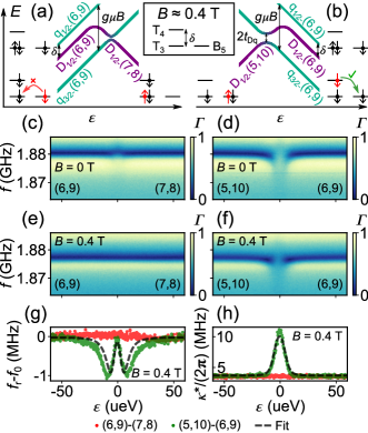
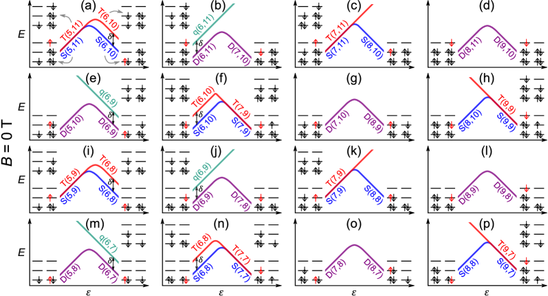
To facilitate the understanding of the non-reciprocal presence of PSB in Figs. 1(c) and (d), we focus on the three outermost electrons in the DQD and sketch the single- and multi-particle energy levels for these electrons. In the (5,10), (6,9) and (7,8) charge states, the three outermost electrons are distributed between the , and energy levels shown in the inset of Figs. 2(a) and (b), where () refers to the energy level of (). By populating the single-particle energy levels with the number of electrons corresponding to the charge state, we observe that the electrons in the DQD may form doublets D with one unpaired electron and a spin angular momentum or quadruplets q with three unpaired electrons and . At T, the ground state D(6,9) is separated from the first excited state q(6,9) by (see Appendices C and F for extraction of and energy spectra at T). However, as is increased, the states Zeeman split according to , where is the spin-angular-momentum projection onto the -axis, is the electron -factor and is the Bohr magneton, thus causing the lowest-energy quadruplet to become the (6,9) ground state when . This situation is sketched in Figs. 2(a) and (b), which show the energy levels of the DQD as a function of detuning at T. From these energy levels, one would expect the ground state electron transitions and , highlighted by the red electrons and arrows in Fig. 2(a) and (b) respectively, to be spin-blocked due to the Pauli exclusion principle. However, recalling Fig. 1, PSB is only present for the (6,9)-(7,8) transition involving levels and , and not for the (5,10)-(6,9) transition, which involves levels and . This hints at a level-selective process that allows spin-flip tunneling as the explanation for the signal generated at the -intersection as a function of .
III Pauli spin blockade lifting Mechanism
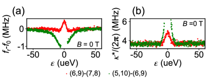
We further investigate the two ICTs by studying the reflected spectrum of the resonator while changing detuning , where is the central position of the measured ICT, at both T and T [see Figs. 2(c)-(f)] [42]. Due to the effective coherent DQD-resonator coupling given by for states and , where in which is assumed constant for a given charge configuration, is the resistance quantum, is the coupling matrix element, and is the charge number operator, we observe changes in the resonance frequency and effective linewidth of the resonator according to [43, 44, 35]
| (1) |
| (2) |
where is the DQD tunnel coupling, is the energy difference between participating states, , is the bare resonator linewidth, and is the DQD decoherence rate. By applying these equations to the measurements in Figs. 2(c)-(f), we can deduce important information about the DQD.
Inspection of the resonator response at T in Fig. 2(c) reveals an upwards shift of around for the (6,9)-(7,8) transition thus indicating and hence the tunnel coupling for states . Despite being in the resonant regime at where , we do not observe characteristic vacuum Rabi-mode-splitting due to the large of this charge transition indicated by the increased around (see Appendix D). By similar inspection of Fig. 2(d), we find a downwards shift of around indicating that and hence that the tunnel coupling for states . To better understand the origin of non-reciprocal PSB, we repeat the resonator response measurements at T as shown in Figs. 2(e) and (f) and furthermore fit each trace of the response to a Lorenzian with centre frequency and linewidth (see Appendix E for description of fitting procedure). As can be seen from the red (6,9)-(7,8) data in Figs. 2(g) and (h), there are no changes to or around , thus indicating that the coupling matrix element . This conclusion agrees with the lack of phase response at T due to PSB seen in Fig. 1(c). However, for the (5,10)-(6,9) transition represented by the green data in Figs. 2(g) and (h), the shift in and increase in around indicates for states . The observation that first decreases symmetrically with decreasing indicates whereas the subsequent increase to at indicates when . This implies a tunnel coupling of , which is confirmed by fitting and simultaneously with shared parameters to Eqs. (1) and (2) from which we obtain , , and . For electrons in silicon, is a remarkably large tunnel coupling between states with different , more than twice the value theoretically estimated in Corna et al [14].
The spin-flip (5,10)-(6,9) charge transition at , confirmed by the non-zero coupling matrix element, is identified as an incoherent tunneling process due to the large increase in the resonator linewidth around . The large indicates that the system decoheres on the timescale of the resonator and hence that the measurable signal at the anti-crossing results from the net charge transfer of multiple incoherent passages. We therefore discard coherent tunneling by adiabatic passage as the origin of the signal, despite the large . Incoherent tunneling may be the consequence of fast state relaxation or pure dephasing. We can further narrow down the origin of the signal by discarding ordinary intradot valley-hotspot-mediated relaxation [45] since this process is highly magnetic field-dependent and hence incompatible with the relatively constant signal seen in Fig. 1(d) and in Appendix B. Whether decoherence is dominated by interdot relaxation or pure dephasing remains to be determined, but given that decoherence is generally dephasing-limited in silicon spin systems we speculate the latter to be the dominant mechanism. The large value of indicates the presence of significant SOC which may open dephasing channels similar to those observed for spin-preserving transitions in corner QDs [46, 47, 48] that are compatible with our measured value of . Additionally, spin, valley, and orbital degrees of freedom may all be mixed on a wide energy range by spin-orbit and valley-orbit couplings, which together with Coulomb interactions provide efficient paths for decoherence. In particular, it has been shown in [49] that anisotropic QDs such as the ones characterised in this work are prone to Wigner-like localization: The electrons split apart in the charged dots due to Coulomb repulsion, which results in a significant compression of the energy spectrum [29] and mixing of the different degrees of freedom in the presence of spin-orbit and valley-orbit coupling mechanisms [50, 51, 52]. Although the observed at the anti-crossing is large, one may expect a reduction away from the anti-crossing where the energy difference of intradot transitions is -independent, thus encouraging coherent EDSR experiments for electron spins in silicon corner dots. Additionally, we note that the spin-blockade-lifting mechanism presented here does not render spin readout impossible but does lead to a reduced and magnetic-field-dependent readout window. In fact, the dispersive signals generated at the anti-crossing points of the different spin manifolds enable positive detection of both the singlet (doublet) at and the triplet (quadruplet ) at through selection of the detuning value at which readout is performed.
IV Prevalence of Pauli spin blockade
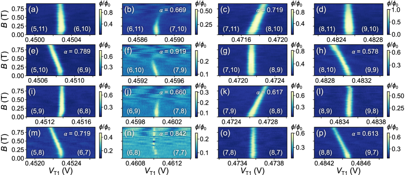
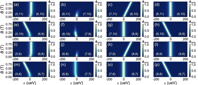
To better understand the prevalence of PSB or lack thereof, we expand the magnetospectroscopy measurements to all 16 ICTs visible in Fig. 1(b). The resulting measurements are shown in Fig. 3 in which panels (e) and (j) represent the measurements studied in Fig. 1. The measurements fall into four categories, which are covered in detail in Appendix F and summarised here: Most abundant for this DQD is the lack of PSB due to fast spin-flip transitions as seen in Figs. 3(c), (e), (f), (h), (k), (m), (n), and (p), among which (f) and (n) are unusual due to the small splitting as explained in Appendix F. Regular PSB on the other hand is only seen in panels (b) and (j), and partial PSB in which large tunnel couplings relative to obscure the blockaded region (see Appendices F and G) found in panels (a) and (i). Finally, Figs. 3(d), (g), (l), and (o) demonstrate cases without PSB in which the spin ground state remains the same for all measured consistent with previously reported odd-parity transitions [36]. Besides the prevalence, we find that the measurements have a periodicity of two in the occupancy, indicating broken valley degeneracy and large level separation in . This agrees with the addition energy that can be inferred from the charge stability diagram and the smaller QD size expected from the lesser channel overlap of . From the sloped magnetospectroscopy measurements in Fig. 3, we extract and find a consistently large average across the ten ICTs involving different spin manifolds.
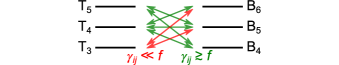
By analysis and simulation of each measurement presented in Fig. 3, we construct energy levels similar to those in Figs. 2(a) and (b) (see Appendices F and G), which enable us to understand which combinations of QD energy levels produce fast spin-flipping. The resulting analysis is summarised in Fig. 4, which shows that all transitions except those that involve level have . The reason for the level-selectivity is unknown, but may be linked to the orbital and valley quantum numbers of the QD states involved.
V Conclusions and outlook
In summary, we have studied the spin-blockade physics of a silicon electron DQD coupled to a resonator probed in reflectometry and through dispersive magnetospectroscopy measurements of 16 ICTs found the presence of PSB to be non-reciprocal and energy-level selective. By analysing the resonator response as a function of DQD detuning and probe frequency using input-output theory, we reported the largest tunnel coupling between different electron spin manifolds yet and determined that the lifting of PSB is due to fast decoherence at the manifold anti-crossing. This finding provides a way of positively detecting both orientations of a spin, e.g. singlets and triplets, through selection of appropriate readout detuning values and may thus enhance readout fidelities. The large , possibly due to enhanced spin-orbit coupling of silicon corner QDs, encourages attempts to perform EDSR away from the anti-crossings followed by readout at the chosen anti-crossing. Overall, our results build a new understanding of PSB physics in silicon important to spin qubit readout and motivate pursuit of all-electrical control of electron spin qubits.
Acknowledgements.
We thank M. Benito and C. Lainé for valuable discussions. This research has received funding from the European Union’s Horizon 2020 Research and Innovation Programme under grant agreements No 688539 and 951852. T.L. acknowledges support from the EPSRC Cambridge NanoDTC, EP/L015978/1. D.J.I. is supported by the Bristol Quantum Engineering Centre for Doctoral Training, EPSRC Grant No. EP/L015730/1. M.F.G.Z. acknowledges support from Industrial Strategy Challenge Fund, UKRI. C.L. and J.W.A.R. acknowledge the EPSRC through the Core-to-Core International Network “Oxide Superspin” (EP/P026311/1) and the “Superconducting Spintronics” Programme Grant (EP/N017242/1).Appendix A Description of device and measurement setup
Figure 1(a) depicts the formation of a DQD in a split-gate nanowire field-effect transistor as well as the resonant circuit used to perform dispersive gate-sensing of the DQD. The transistor, which is fabricated on a 300-mm fully-depleted silicon-on-insulator wafer with a buried oxide (BOX) thickness of 145 nm, consists of a nm thick, nm wide silicon nanowire channel, a 6 nm SiO2 gate oxide and two TiN/polysilicon gates, G and G, with 60 nm gate lengths and a nm split-gate separation. We note that G overlaps the channel slightly more than G due to a nm misalignment during fabrication. Spacers made of Si3N4 are used to extend the region of intrinsic silicon beneath the gates by 34 nm on either side, thus creating tunnel barriers to the heavily n-type-doped source and drain that are held at 0 V. To facilitate gate-based sensing, G is wirebonded to a superconducting NbN spiral inductor on a separate chip, thus forming a resonant circuit comprised of the capacitance from G to ground, parasitic capacitance , and magnetic-field-dependent inductance of the spiral. At T, the resonator has a resonance frequency of GHz, however when the magnetic field is increased, the resonance frequency decreases due to the increasing kinetic inductance of the superconducting spiral inductor [29]. The inductor, which is fabricated by optical lithography of an 80-nm-thick sputter-deposited NbN film on a sapphire substrate, is situated adjacent to a 50 microstrip waveguide and designed to achieve critical coupling between the resonator and input line. This design results in a large resonator characteristic impedance which, together with the large lever arm of the wrap-around gates (where is the capacitance between gate and QD and is the total capacitance of QD ), enables a large coherent coupling rate and thus a large signal-to-noise ratio [35]. We probe the resonator-DQD system in reflectometry via the microwave transmission line labelled MW in Fig. 1.
Appendix B Maximum phase shift of (5,10)-(6,9) ICT vs magnetic field
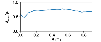
To further characterise the lack of Pauli spin blockade (PSB) observed for the (5,10)-(6,9) ICT in the magnetospectroscopy measurement of Figs. 1(d) and 3(e), we extract the maximum relative phase shift , where is the largest phase shift measured among the 16 ICTs in Fig. 1(b), for each -field linetrace as seen in Fig. 5. With the exception of a small decrease around mT, Fig. 5 shows that remains relatively constant from to . As explained in the main text, the constant phase shift rules out magnetic-field-dependent processes such as standard intradot valley-mediated-relaxation [45] as the explanation for the lack of PSB. We note that the decreased phase shift around mT is also observed in magnetospectroscopy measurements of all the other ICTs in Fig. 3. We attribute the decrease in phase shift to a reduction of the resonator Q-factor around mT. This deterioration of the Q-factor is also observed in measurements of the reflected spectrum of the resonator as a function of magnetic field during which the device is grounded.
Appendix C Extracting T3-T4 energy separation
As can be seen from Fig. 2, the D(6,9)-q(6,9) energy separation is given by the splitting of levels T3 and T4. The magnitude of may be extracted from the magnetospectroscopy measurement presented in Fig. 6 [same data as shown in Figs. 1(d) and 3(e)] by extrapolating the sloped signal of the D(5,10)-q(6,9) anti-crossing to T and determining the voltage separation of the extrapolated signal from the doublet anti-crossing signal at T. To extrapolate the signal of the D(5,10)-q(6,9) anti-crossing, we extract the centre of the phase shift peak for each line trace above T and linearly fit these points to obtain the solid red line in Fig. 6. From the intersection of the linear fit with T and the central position of the phase shift signal at T marked with a dotted red line in Fig. 6, we find a voltage separation of , which entails .
Appendix D Resonator response for ICTs (6,9)-(7,8) and (5,10)-(6,9) at B=0 T
To emphasise the features of the resonator response at T shown in Figs. 2(c) and (d), we perform the same analysis and Lorentzian fitting as for Figs. 2(e) and (f) and as is described in Appendix E. The and values obtained for the fits are plotted in Fig. 7. From Fig. 7(a) it is immediately clear that the resonance shifts up [down] for ICT (6,9)-(7,8) [(5,10)-(6,9)], thus providing further evidence for the observations made in the main text that and . From Fig. 7(b), we note a sizeable increase in around indicating a large decoherence rates and for the (6,9)-(7,8) and (5,10)-(6,9) doublet transitions. This explains the absence of vacuum Rabi-mode-splitting, which may otherwise have been expected for the resonant regime of ICT (6,9)-(7,8) at T. The large also complicates fitting the resonator response of ICT (5,10)-(6,9) around to Eq. (3) and is therefore the reason for the lacking data points around in Fig. 7. We note that is smaller than indicating that in this device coupling between states with the same spin angular momentum can be smaller than between states with different .
Appendix E Description of fitting procedures
For the analysis of the resonator response as a function of detuning , we use the steady-state power reflection coefficient developed from the Heisenberg-Langevin equations of motion in its complex Lorentzian form [35]
| (3) |
where MHz is the external photon decay rate, and where as well as are defined in Eqs. (1) and (2) in the main text. To obtain the values for and plotted in Figs. 2(g) and (h) as well as Figs. 7(a) and (b) below, we fit each line trace of the data presented in Figs. 2(c)-(f) to Eq. (3).
We use the and data at T plotted in Figs. 2(g) and (h) to extract the coherent coupling rate , tunnel coupling , and decoherence rate . This is done by simultaneously fitting and to Eqs. (1) and (2) in the main text with shared fitting parameters , , and and using orthogonal distance regression (ODR) that factors in the errors on both axis for each dataset. The errors given for , , and in the main text are obtained from the covariance matrix of the ODR fit and represent one standard deviation.
Appendix F Energy-level diagrams for all 16 ICTs at B=0 T and B=0.4 T
Figures 8 and 9 sketch the single-particle and DQD energy levels as a function of detuning at T and T, respectively, for all 16 ICTs visible in the charge stability diagram of Fig. 1(b). The single-particle energy levels shown in each panel of Figs. 8 and 9 represent the six energy levels shown in Fig. 4, which means that the two (three) lowest and fully-occupied energy levels of QD (QD) have been omitted for simplicity. The electrons highlighted in red in the single-particle energy diagrams indicate which electrons move QD when crossing an ICT, whereas the presence of a green (red) arrow indicates the presence (lack) of spin-flip tunneling. The colour of the DQD energy levels indicate the multiplicity of the multi-particle spin state it represents, and for simplicity, couplings between manifolds of different spin angular momentum are not included in the sketch. To strengthen the link to the main text, the panels of Figs. 8 and 9 are organised such that they match the location of the ICTs in the charge stability diagram as well as the panel labels of Fig. 3. This means that one electron is added to QD (QD) when moving one panel to the right (up). One may note from the first and second column of panels in Figs. 8 and 9, that the small splitting is a defining feature which, for example, explains the presence of the low-energy quadruplet states. In the following, we split the energy diagrams into groups with similar features and use them as a basis for explaining the corresponding magnetospectroscopy panels of Fig. 3:
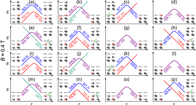
Panels (c), (e), (f), (h), (k), (m), (n), and (p)
As highlighted in the main text and as seen in the case of Fig. 3(c), (e), (f), (h), (k), (m), (n), and (p), the lack of PSB is most abundant among the 16 ICTs. For panels (c), (h), (k), and (p), the phase shift signal of the magnetospectroscopy slopes to one side already from T. This indicates that the signal at arises from the anti-crossing of singlets [see Fig. 8(c), (h), (k), and (f)], but that the singlet tunnel coupling is small such that the signal at T arises from incoherent tunneling between the singlet and triplet states as indicated by the green arrows in Fig. 9(c), (h), (k), and (f).
Panels (e) and (m) are similar to panels (c), (h), (k), and (p), but involve doublet and quadruplet spin states instead of singlets and triplets. Whereas the singlets and triplets were degenerate in one charge configuration at T, the minimal energy difference between the doublet and quadruplet is given by . The signal at T from the doublet anti-crossing [see Fig. 8(e) and (m)] therefore persists for longer, and only when T do the quadruplets start to intersect the doublets, resulting in the characteristic sloped signal arising from incoherent tunneling.
Panels (f) and (n) start off similar to panels (c), (h), (k), and (p) with the explanation for what happens in the low-field region of the magnetospectroscopy being the same. However, as seen in Fig. 8(f) and (n), the maximal separation of the triplets from the singlets is , which means that the triplets become the ground state when T. The straight high-field signal in Fig. 3(n) may therefore attributed to the anti-crossing triplet ground state [see Fig. 9(n)], whereas the lack of any high-field signal in Fig. 3(f) may be explained by the tunnel coupling of the anti-crossing triplet states being so small that the resonator probe drives diabatic Landau-Zener transitions across the anti-crossing [53].
Panels (b) and (j)
The only two cases of clear PSB are found in panels (b) and (j), which involve doublet and quadruplet states, and whose magnetospectroscopy matches previous observations of dispersively-detected PSB [36, 24, 38, 39, 40]. Similar to panels (e) and (m), the low-field signal arises from the doublet anti-crossing [see Figs. 8(b) and (j)], and only when T does PSB begin to manifest because spin-flip tunneling is prohibited for energy-level transitions T3-B5 and T3-B6 as shown with the red arrows in Figs. 9(b) and (j).
Panels (a) and (i)
Panels (a) and (i) bear similarities with panels (f) and (n) because the triplet anti-crossing also here becomes the ground state already when T, giving rise to the high-field signal [see Figs. 9(a) and (i)]. However, because the tunnel coupling of both the singlet and triplet manifolds is large compared to for panels (a) and (i), we do not observe a region of no-signal PSB that would otherwise have expected from the energy-level transitions T3-B5 and T3-B6. We therefore classify these two panels as cases of partial PSB.
Panels (d), (g), (l), and (o)
Finally, panels (d), (g), (l), and (o) represent simple cases of odd-parity transitions [36] where the anti-crossing of just one spin manifold, the doublet, is the ground state for the entire range of magnetic fields studied. The lack of any higher spin manifolds indicates that the energy-level separation between levels T4 and T5 as well as the separation between levels in QD greater than , i.e. substantially larger than .
Appendix G Magnetospectroscopy simulations for all 16 ICTs
To support the explanations of the observed magnetospectroscopy provided in Appendix F, we qualitatively simulate the resonator response as a function of magnetic field for the energy spectra in Figs. 8 and 9. We use the semi-classical approximation [32] where the effect of the quantum system on a classical resonator is expressed in terms of the parametric capacitance
| (4) |
where is the electron charge, is the interdot lever arm, is the occupation probability of the QD connected to the resonator. We further consider the small signal regime where the phase response of the resonator is directly proportional to the change in parametric capacitance, . The QD occupation probability can be expanded in terms of the polarization and occupation probabilities of each individual eigenstate, and respectively
| (5) |
In this case, the parametric capacitance can be expanded in terms of its two principal constituents, the quantum capacitance and tunneling capacitance [32, 54]:
| (6) |
Finally, to perform the simulations we consider the general expression of the polarizations:
| (7) |
To produce the simulations, the parameters that are needed are the couplings between eigenenergies in the same spin branch , the energy splittings at large absolute detuning and the temperature . In each panel, we either use the slow relaxation regime, where only quantum capacitance manifests, or the fast relaxation regime, where both quantum and tunneling capacitance contribute to the total parametric capacitance [32]. The latter implies that we are simulating fast decoherence via relaxation and hence we use the thermal probabilities . Table 1 summarises the parameters used to simulate each of the 16 energy spectra. Columns two and three list the tunnel couplings in between the spin manifolds present in the energy spectrum at the given charge occupation (see Appendix F), whereas columns four and five list the energy splittings in at large negative (positive) detuning (). Note that values of simply indicate that the splitting is larger than and hence renders the high-spin anti-crossing unobservable within the measured and simulated range of magnetic fields. Finally, the last column denotes the relaxation regime simulated, i.e. whether tunneling capacitance is included or not. We use a temperature of mK for all simulations and for all splittings that correspond to the T3-T4 separation .
Based on the proportionality , we use Eqs. (6) and (7) and the parameters in Table 1 to qualitatively simulate the normalised phase shift and magnetospectra for the energy spectra sketched in Figs. 8 and 9. The simulation results are shown in Fig. 10. For the simulation of Fig. 10(f), we introduce a suppression of the phase shift signal for T to account for Landau-Zener transitions which cause the change in QD occupation probability to approach zero. Overall, the simulations represent the measured magnetospectra in Fig. 3 well.
| Panel | or (eV) | or (eV) | (eV) | (eV) | Relaxation regime |
| a | 20 | 20 | 0 | 18 | Slow |
| b | 15 | 20 | 18 | >120 | Slow |
| c | 10 | 20 | 0 | >120 | Fast |
| d | 20 | 20 | >120 | >120 | Fast |
| e | 20 | 20 | >120 | 18 | Fast |
| f | 10 | 3 | 18 | 0 | Fast |
| g | 20 | 20 | >120 | >120 | Fast |
| h | 10 | 20 | >120 | 0 | Fast |
| i | 20 | 20 | 0 | 18 | Slow |
| j | 7 | 20 | 18 | >120 | Slow |
| k | 10 | 20 | 0 | >120 | Fast |
| l | 20 | 20 | >120 | >120 | Fast |
| m | 20 | 20 | >120 | 18 | Fast |
| n | 10 | 20 | 18 | 0 | Fast |
| o | 20 | 20 | >120 | >120 | Fast |
| p | 10 | 20 | >120 | 0 | Fast |
References
- Loss and DiVincenzo [1998] D. Loss and D. P. DiVincenzo, Quantum computation with quantum dots, Phys. Rev. A 57, 120 (1998).
- Veldhorst et al. [2014] M. Veldhorst, J. C. C. Hwang, C. H. Yang, A. W. Leenstra, B. de Ronde, J. P. Dehollain, J. T. Muhonen, F. E. Hudson, K. M. Itoh, A. Morello, et al., An addressable quantum dot qubit with fault-tolerant control-fidelity, Nat. Nanotechnol. 9, 981 (2014).
- Yang et al. [2019] C. H. Yang, K. W. Chan, R. Harper, W. Huang, T. Evans, J. C. C. Hwang, B. Hensen, A. Laucht, T. Tanttu, F. E. Hudson, et al., Silicon qubit fidelities approaching incoherent noise limits via pulse engineering, Nat. Electron. 2, 151 (2019).
- Petit et al. [2020] L. Petit, H. G. J. Eenink, M. Russ, W. I. L. Lawrie, N. W. Hendrickx, S. G. J. Philips, J. S. Clarke, L. M. K. Vandersypen, and M. Veldhorst, Universal quantum logic in hot silicon qubits, Nature 580, 355 (2020).
- Yang et al. [2020] C. H. Yang, R. C. C. Leon, J. C. C. Hwang, A. Saraiva, T. Tanttu, W. Huang, J. C. Lemyre, K. W. Chan, K. Y. Tan, F. E. Hudson, et al., Operation of a silicon quantum processor unit cell above one kelvin, Nature 580, 350 (2020).
- Camenzind et al. [2021] L. C. Camenzind, S. Geyer, A. Fuhrer, R. J. Warburton, D. M. Zumbühl, and A. V. Kuhlmann, A spin qubit in a fin field-effect transistor, arXiv:2103.07369 (2021).
- Maurand et al. [2016] R. Maurand, X. Jehl, D. Kotekar-Patil, A. Corna, H. Bohuslavskyi, R. Laviéville, L. Hutin, S. Barraud, M. Vinet, M. Sanquer, et al., A CMOS silicon spin qubit, Nat. Commun. 7, 13575 (2016).
- Zwerver et al. [2021] A. M. J. Zwerver, T. Krähenmann, T. F. Watson, L. Lampert, H. C. George, R. Pillarisetty, S. A. Bojarski, P. Amin, S. V. Amitonov, J. M. Boter, et al., Qubits made by advanced semiconductor manufacturing, arXiv:2101.12650 (2021).
- Li et al. [2020] R. Li, N. I. D. Stuyck, S. Kubicek, J. Jussot, B. T. Chan, F. A. Mohiyaddin, A. Elsayed, M. Shehata, G. Simion, C. Godfrin, et al., A flexible 300 mm integrated Si MOS platform for electron-and hole-spin qubits exploration, in 2020 IEEE International Electron Devices Meeting (IEDM) (IEEE, 2020) pp. 33–38.
- Xue et al. [2021] X. Xue, B. Patra, J. P. G. van Dijk, N. Samkharadze, S. Subramanian, A. Corna, B. P. Wuetz, C. Jeon, F. Sheikh, E. Juarez-Hernandez, et al., CMOS-based cryogenic control of silicon quantum circuits, Nature 593, 205 (2021).
- Pauka et al. [2019] S. J. Pauka, K. Das, R. Kalra, A. Moini, Y. Yang, M. Trainer, A. Bousquet, C. Cantaloube, N. Dick, G. C. Gardner, et al., A cryogenic interface for controlling many qubits, arXiv:1912.01299 (2019).
- Veldhorst et al. [2017] M. Veldhorst, H. G. J. Eenink, C. H. Yang, and A. S. Dzurak, Silicon CMOS architecture for a spin-based quantum computer, Nat. Commun. 8, 1766 (2017).
- Huang et al. [2017] W. Huang, M. Veldhorst, N. M. Zimmerman, A. S. Dzurak, and D. Culcer, Electrically driven spin qubit based on valley mixing, Phys. Rev. B 95, 075403 (2017).
- Corna et al. [2018] A. Corna, L. Bourdet, R. Maurand, A. Crippa, D. Kotekar-Patil, H. Bohuslavskyi, R. Laviéville, L. Hutin, S. Barraud, X. Jehl, et al., Electrically driven electron spin resonance mediated by spin–valley–orbit coupling in a silicon quantum dot, npj Quantum Inf. 4, 6 (2018).
- Ahmed et al. [2018] I. Ahmed, J. A. Haigh, S. Schaal, S. Barraud, Y. Zhu, C.-m. Lee, M. Amado, J. W. A. Robinson, A. Rossi, J. J. L. Morton, and M. F. Gonzalez-Zalba, Radio-Frequency Capacitive Gate-Based Sensing, Phys. Rev. Applied 10, 014018 (2018).
- West et al. [2019] A. West, B. Hensen, A. Jouan, T. Tanttu, C.-H. Yang, A. Rossi, M. F. Gonzalez-Zalba, F. Hudson, A. Morello, D. J. Reilly, et al., Gate-based single-shot readout of spins in silicon, Nat. Nanotechnol. 14, 437 (2019).
- Crippa et al. [2019] A. Crippa, R. Ezzouch, A. Aprá, A. Amisse, L. Houtin, B. Bertrand, M. Vinet, M. Urdampilleta, T. Meunier, M. Sanquer, et al., Gate-reflectometry dispersive readout and coherent control of a spin qubit in silicon, Nat. Commun. 10, 2776 (2019).
- Pakkiam et al. [2018] P. Pakkiam, A. V. Timofeev, M. G. House, M. R. Hogg, T. Kobayashi, M. Koch, S. Rogge, and M. Y. Simmons, Single-Shot Single-Gate rf Spin Readout in Silicon, Phys. Rev. X 8, 041032 (2018).
- Ono et al. [2002] K. Ono, D. G. Austing, Y. Tokura, and S. Tarucha, Current rectification by Pauli exclusion in a weakly coupled double quantum dot system, Science 297, 1313 (2002), arXiv:0208001v1 [arXiv:astro-ph] .
- Elzerman et al. [2004] J. M. Elzerman, R. Hanson, L. H. W. Van Beveren, B. Witkamp, L. M. K. Vandersypen, and L. P. Kouwenhoven, Single-shot read-out of an individual electron spin in a quantum dot, Nature 430, 431 (2004).
- Schoelkopf et al. [1998] R. J. Schoelkopf, P. Wahlgren, A. A. Kozhevnikov, P. Delsing, and D. E. Prober, The radio-frequency single-electron transistor (RF-SET): A fast and ultrasensitive electrometer, Science 280, 1238 (1998).
- Huang et al. [2021] J. Y. Huang, W. H. Lim, R. C. C. Leon, C. H. Yang, F. E. Hudson, C. C. Escott, A. Saraiva, A. S. Dzurak, and A. Laucht, A High-Sensitivity Charge Sensor for Silicon Qubits above 1 K, Nano Lett. (2021).
- Ciriano-Tejel et al. [2021] V. N. Ciriano-Tejel, M. A. Fogarty, S. Schaal, L. Hutin, B. Bertrand, L. Ibberson, M. F. Gonzalez-Zalba, J. Li, Y.-M. Niquet, M. Vinet, and J. J. L. Morton, Spin Readout of a CMOS Quantum Dot by Gate Reflectometry and Spin-Dependent Tunneling, PRX Quantum 2, 010353 (2021).
- Betz et al. [2015] A. C. Betz, R. Wacquez, M. Vinet, X. Jehl, A. L. Saraiva, M. Sanquer, A. J. Ferguson, and M. F. Gonzalez-Zalba, Dispersively detected Pauli spin-blockade in a silicon nanowire field-effect transistor, Nano Lett. 15, 4622 (2015).
- Zheng et al. [2019] G. Zheng, N. Samkharadze, M. L. Noordam, N. Kalhor, D. Brousse, A. Sammak, G. Scappucci, and L. M. K. Vandersypen, Rapid gate-based spin read-out in silicon using an on-chip resonator, Nat. Nanotechnol. 14, 742 (2019).
- Zhao et al. [2019] R. Zhao, T. Tanttu, K. Y. Tan, B. Hensen, K. W. Chan, J. C. C. Hwang, R. C. C. Leon, C. H. Yang, W. Gilbert, F. E. Hudson, et al., Single-spin qubits in isotopically enriched silicon at low magnetic field, Nat. Commun. 10, 5500 (2019).
- Fogarty et al. [2018] M. A. Fogarty, K. W. Chan, B. Hensen, W. Huang, T. Tanttu, C. H. Yang, A. Laucht, M. Veldhorst, F. E. Hudson, K. M. Itoh, et al., Integrated silicon qubit platform with single-spin addressability, exchange control and single-shot singlet-triplet readout, Nat. Commun. 9, 4370 (2018).
- Harvey-Collard et al. [2018] P. Harvey-Collard, B. D’Anjou, M. Rudolph, N. T. Jacobson, J. Dominguez, G. A. TenEyck, J. R. Wendt, T. Pluym, M. P. Lilly, W. A. Coish, et al., High-fidelity single-shot readout for a spin qubit via an enhanced latching mechanism, Phys. Rev. X 8, 021046 (2018).
- Lundberg et al. [2020] T. Lundberg, J. Li, L. Hutin, B. Bertrand, D. J. Ibberson, C.-M. Lee, D. J. Niegemann, M. Urdampilleta, N. Stelmashenko, T. Meunier, et al., Spin Quintet in a Silicon Double Quantum Dot: Spin Blockade and Relaxation, Phys. Rev. X 10, 041010 (2020).
- Seedhouse et al. [2021] A. E. Seedhouse, T. Tanttu, R. C. C. Leon, R. Zhao, K. Y. Tan, B. Hensen, F. E. Hudson, K. M. Itoh, J. Yoneda, C. H. Yang, et al., Pauli blockade in silicon quantum dots with spin-orbit control, PRX Quantum 2, 010303 (2021).
- van der Heijden et al. [2018] J. van der Heijden, T. Kobayashi, M. G. House, J. Salfi, S. Barraud, R. Laviéville, M. Y. Simmons, and S. Rogge, Readout and control of the spin-orbit states of two coupled acceptor atoms in a silicon transistor, Sci. Adv. 4, eaat9199 (2018).
- Mizuta et al. [2017] R. Mizuta, R. M. Otxoa, A. C. Betz, and M. F. Gonzalez-Zalba, Quantum and tunneling capacitance in charge and spin qubits, Phys. Rev. B 95, 045414 (2017).
- Fujita et al. [2016] T. Fujita, P. Stano, G. Allison, K. Morimoto, Y. Sato, M. Larsson, J.-H. Park, A. Ludwig, A. D. Wieck, A. Oiwa, and S. Tarucha, Signatures of hyperfine, spin-orbit, and decoherence effects in a Pauli spin blockade, Phys. Rev. Lett. 117, 206802 (2016).
- Petersson et al. [2010] K. D. Petersson, C. G. Smith, D. Anderson, P. Atkinson, G. A. C. Jones, and D. A. Ritchie, Charge and spin state readout of a double quantum dot coupled to a resonator, Nano Lett. 10, 2789 (2010).
- Ibberson et al. [2021] D. J. Ibberson, T. Lundberg, J. A. Haigh, L. Hutin, B. Bertrand, S. Barraud, C.-M. Lee, N. A. Stelmashenko, J. W. A. Robinson, M. Vinet, et al., Large Dispersive Interaction between a CMOS Double Quantum Dot and Microwave Photons, PRX Quantum 2, 020315 (2021).
- Schroer et al. [2012] M. D. Schroer, M. Jung, K. D. Petersson, and J. R. Petta, Radio frequency charge parity meter, Phys. Rev. Lett. 109, 166804 (2012).
- House et al. [2015] M. G. House, T. Kobayashi, B. Weber, S. J. Hile, T. F. Watson, J. Van Der Heijden, S. Rogge, and M. Y. Simmons, Radio frequency measurements of tunnel couplings and singlet-triplet spin states in Si:P quantum dots, Nat. Commun. 6, 8848 (2015).
- Urdampilleta et al. [2015] M. Urdampilleta, A. Chatterjee, C. C. Lo, T. Kobayashi, J. Mansir, S. Barraud, A. C. Betz, S. Rogge, M. F. Gonzalez-zalba, and J. J. L. Morton, Charge Dynamics and Spin Blockade in a Hybrid Double Quantum Dot in Silicon, Phys. Rev. X 5, 031024 (2015).
- Landig et al. [2019] A. J. Landig, J. V. Koski, P. Scarlino, C. Reichl, W. Wegscheider, A. Wallraff, K. Ensslin, and T. Ihn, Microwave-Cavity-Detected Spin Blockade in a Few-Electron Double Quantum Dot, Phys. Rev. Lett. 122, 213601 (2019).
- Hutin et al. [2019] L. Hutin, B. Bertrand, E. Chanrion, H. Bohuslavskyi, F. Ansaloni, T. . Yang, J. Michniewicz, D. J. Niegemann, C. Spence, T. Lundberg, A. Chatterjee, A. Crippa, J. Li, R. Maurand, X. Jehl, M. Sanquer, M. F. Gonzalez-Zalba, F. Kuemmeth, Y.-M. Niquet, S. De Franceschi, M. Urdampilleta, T. Meunier, and M. Vinet, Gate reflectometry for probing charge and spin states in linear Si MOS split-gate arrays, in 2019 IEEE International Electron Devices Meeting (IEDM) (2019) pp. 37.7.1–37.7.4.
- Johnson et al. [2005] A. C. Johnson, J. R. Petta, C. M. Marcus, M. P. Hanson, and A. C. Gossard, Singlet-triplet spin blockade and charge sensing in a few-electron double quantum dot, Phys. Rev. B 72, 165308 (2005).
- Petersson et al. [2012] K. D. Petersson, L. W. Mcfaul, M. D. Schroer, M. Jung, J. M. Taylor, A. A. Houck, and J. R. Petta, Circuit quantum electrodynamics with a spin qubit, Nature 490, 380 (2012).
- Childress et al. [2004] L. Childress, A. S. Sørensen, and M. D. Lukin, Mesoscopic cavity quantum electrodynamics with quantum dots, Phys. Rev. A 69, 042302 (2004).
- Koch et al. [2007] J. Koch, T. M. Yu, J. Gambetta, A. A. Houck, D. I. Schuster, J. Majer, A. Blais, M. H. Devoret, S. M. Girvin, and R. J. Schoelkopf, Charge-insensitive qubit design derived from the Cooper pair box, Phys. Rev. A 76, 042319 (2007).
- Yang et al. [2013] C. H. Yang, A. Rossi, R. Ruskov, N. S. Lai, F. A. Mohiyaddin, S. Lee, C. Tahan, G. Klimeck, A. Morello, and A. S. Dzurak, Spin-valley lifetimes in a silicon quantum dot with tunable valley splitting, Nat. Commun. 4, 1 (2013).
- Dupont-Ferrier et al. [2013] E. Dupont-Ferrier, B. Roche, B. Voisin, X. Jehl, R. Wacquez, M. Vinet, M. Sanquer, and S. De Franceschi, Coherent coupling of two dopants in a silicon nanowire probed by Landau-Zener-Stückelberg interferometry, Phys. Rev. Lett. 110, 136802 (2013).
- Gonzalez-Zalba et al. [2016] M. F. Gonzalez-Zalba, S. N. Shevchenko, S. Barraud, J. R. Johansson, A. J. Ferguson, F. Nori, and A. C. Betz, Gate-sensing coherent charge oscillations in a silicon field-effect transistor, Nano Lett. 16, 1614 (2016).
- Chatterjee et al. [2018] A. Chatterjee, S. N. Shevchenko, S. Barraud, R. M. Otxoa, F. Nori, J. J. L. Morton, and M. F. Gonzalez-Zalba, A silicon-based single-electron interferometer coupled to a fermionic sea, Phys. Rev. B 97, 045405 (2018).
- Abadillo-Uriel et al. [2021] J. C. Abadillo-Uriel, B. Martinez, M. Filippone, and Y.-M. Niquet, Wigner molecularization in asymmetric quantum dots, arXiv:2107.11117 (2021).
- Ercan et al. [2021a] H. E. Ercan, S. N. Coppersmith, and M. Friesen, Strong electron-electron interactions in Si/SiGe quantum dots, arXiv:2105.10645 (2021a).
- Ercan et al. [2021b] H. E. Ercan, M. Friesen, and S. N. Coppersmith, Charge-noise resilience of two-electron quantum dots in Si/SiGe heterostructures, arXiv:2105.10643 (2021b).
- Corrigan et al. [2021] J. Corrigan, J. P. Dodson, H. E. Ercan, J. C. Abadillo-Uriel, B. Thorgrimsson, T. J. Knapp, N. Holman, T. McJunkin, S. F. Neyens, E. R. MacQuarrie, et al., Coherent control and spectroscopy of a semiconductor quantum dot Wigner molecule, Phys. Rev. Lett. 127, 127701 (2021).
- Nielsen et al. [2013] E. Nielsen, E. Barnes, J. P. Kestner, and S. Das Sarma, Six-electron semiconductor double quantum dot qubits, Phys. Rev. B 88, 195131 (2013).
- Esterli et al. [2019] M. Esterli, R. M. Otxoa, and M. F. Gonzalez-Zalba, Small-signal equivalent circuit for double quantum dots at low-frequencies, Appl. Phys. Lett. 114, 253505 (2019).