Te-doped selective-area grown InAs nanowires for superconducting hybrid devices
Abstract
Semiconductor nanowires have emerged as versatile components in superconducting hybrid devices for Majorana physics and quantum computing. The transport properties of nanowires can be tuned either by field-effect or doping. We investigated a series of InAs nanowires which conductivity has been modified by -type doping using tellurium. In addition to electron microscopy studies, the wires were also examined with atomic probe tomography to obtain information about the local incorporation of Te atoms. It was found that the Te atoms mainly accumulate in the core of the nanowire and at the corners of the {110} side facets. The efficiency of -type doping was also confirmed by transport measurements. As a demonstrator hybrid device, a Josephson junction was fabricated using a nanowire as a weak link. The corresponding measurements showed a clear increase of the critical current with increase of the dopant concentration.
I Introduction
InAs nanowires have proven to be suitable consituents for various electronic devicesDayeh et al. (2007); Tomioka et al. (2007); Thelander et al. (2008); Burke et al. (2015) and also for studying fundamental quantum physics phenomena in nanoscale structures.Fasth et al. (2005); Fuhrer et al. (2007); Heedt et al. (2016, 2017); Iorio et al. (2019); Bordoloi et al. (2020) Recently, InAs nanowires attracted attention by their integration in semiconductor-superconductor hybrid structures. A prominent example is the effort regarding the realization of Majorana fermions for topological quantum computing.Mourik et al. (2012); Aguado (2017) In addition, InAs nanowires can serve as a weak link in gate-controlled Josephson junctionsDoh et al. (2005); Günel et al. (2012) for superconducting qubits such as transmonsLarsen et al. (2015); de Lange et al. (2015) or Andreev level qubits.Zazunov et al. (2003)
Due to the Fermi level pinning within the conduction band in InAs, a surface accumulation layer forms naturally,Wieder (1974) ensuring that the nanowire is conductive even without doping. In some cases, however, the ability to control conductivity through doping is desired, e.g. for adjusting the channel conductance in field-effect transistors. Nanowire conductivity has also a great impact on the critical current of Josephson junctions based on InAs nanowiresGünel et al. (2012) and therefore it is a crucial design parameter for the aforementioned qubit circuits.
In most cases, Si is employed as an -type dopant in InAs nanowires.Sladek et al. (2010); Wirths et al. (2011); Ghoneim et al. (2012); Dimakis et al. (2013); Park et al. (2015) Using Si doping, densities in the order of cm-3 are achieved.Wirths et al. (2011); Ghoneim et al. (2012) However, apart from the increase of the carrier concentration in the nanowire, Si doping affects the growth kinetics as well as the nanowire dimensions.Wirths et al. (2011); Dimakis et al. (2013) In GaAs, Te is known as a very effective -type dopant.Sankaran (1980); Kamp et al. (1994); Bennett et al. (2003) As a group VI element Te shows no amphoteric behavior as it is the case for Si in GaAs. As a matter of fact, Te doping already found its applications in -type doped GaAs nanowires.Wallentin and Borgström (2011); Orrù et al. (2016); Goktas et al. (2018); Hakkarainen et al. (2019) Recently, it was demonstrated that Te is also a very efficient dopant in InAs nanowires.Güsken et al. (2019)
To explore the suitability of Te-doped nanowires in superconductor/nanowire hybrid structures, we have grown a series of nanowires with different doping using selective-area molecular beam epitaxy (MBE). The structural properties are investigated by electron microscopy. Detailed information about the dopant distribution in the nanowires is obtained by atom probe tomography (APT). Electrical transport measurements are performed both at room temperature and at 4 K to determine the doping efficiency. Finally, the properties of the doped nanowires for superconducting hybrid structures are investigated by fabricating and measuring nanowire-based Josephson junctions.
II Growth and Device Fabrication
The InAs nanowires were grown by MBE using selective area growth on a Si(111) wafer covered by a 20-nm-thick thermally oxidized SiO2 layer.Koblmüller et al. (2010); Perla et al. (2021) By means of electron beam lithography, hole arrays with a pitch of 1 m and hole diameter of 80 nm are patterned. The holes are etched by reactive ion etching to a depth of roughly 16 nm followed by cleaning in piranha solution (H2SO4:H2O). Immediately before growth, an etching step of 60 s in HF is performed in order to remove the remaining SiO2 in the holes without damaging the Si(111) surface below.
The InAs nanowires are grown without any catalyst via the vapor-solid mechanism ∘C.Rieger et al. (2013) The tellurium is supplied by a GaTe cell. For the first min, a substrate temperature of 480 ∘C, an In growth rate of m/h and an As beam equivalent pressure (BEP) of mbar are used to sustain the nanowire self-seeding. The nanowire growth is then proceeded with a lower substrate temperature of C and In growth rate of m/h. For growth runs A to D the As4 BEP varied between mbar for h depending on the Te doping concentration to avoid changes in the morphology of the nanowires.Güsken et al. (2019) Here, the Te concentration has been varied between and cm-3 by varying the GaTe cell temperature between C and C based on calibrations conducted on Te-doped GaAs layers via Hall-measurements. In addition, two samples were grown with a lower As4 BEP of torr (growth runs E and F) with a nominal doping of and cm-3, respectively. The parameters of the Te-doped InAs nanowires are summarized in table 1.
| growth run | Te-doping | GeTe cell | As4 BEP | length | diameter | ||
|---|---|---|---|---|---|---|---|
| () | (∘C) | (torr) | (m) | (nm) | () | () | |
| A | 420 | ||||||
| B | 437 | n.a. | |||||
| C | 478 | ||||||
| D | 497 | ||||||
| E | 478 | ||||||
| F | 520 |
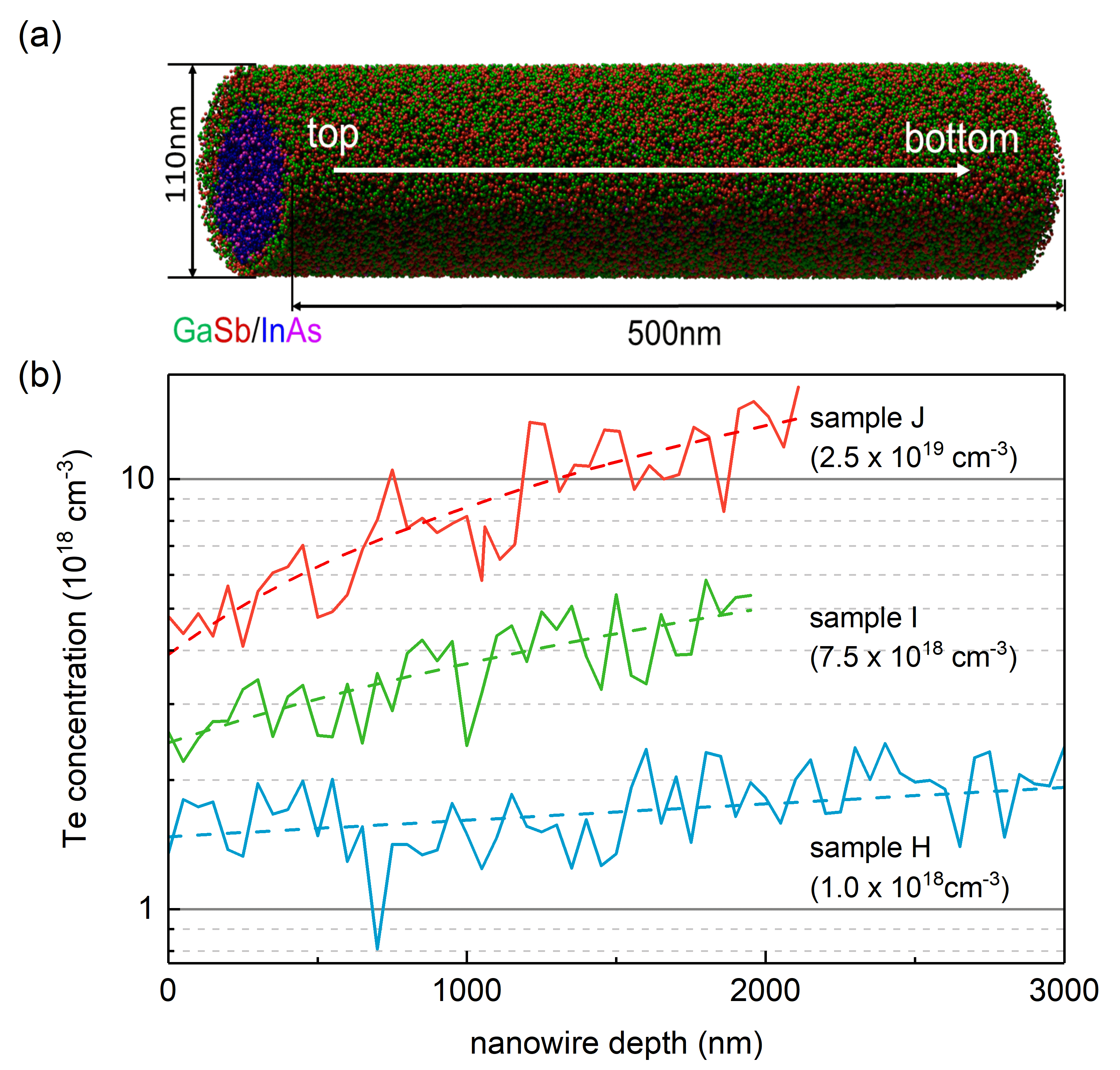
For the APT measurements discussed below, we also prepared InAs nanowires with different doping concentrations, which are covered by a 50-nm-thick GaSb shell (cf. Table 2). The GaSb shell ensures that all atoms of the cross section of the InAs nanowire are gathered by the APT detector.
| Growth run | Te-doping | Te (APT) |
|---|---|---|
| () | () | |
| H | ||
| I | ||
| J |
Specific devices with ohmic contacts have been fabricated for electrical characterisation of InAs nanowires with varying Te-doping levels from growth runs A-F. The nanowires have been transferred mechanically using a clean paper tip to highly doped Si substrates covered by a 200 nm thick thermal SiO2 layer in order to provide a global back gate. On top of the SiO2 layer, metallic contact pads and alignment markers have been placed using optical lithography and lift-off processes. Electrical contacts were defined in a four-terminal configuration by electron beam lithography. The contacts consisted of non-alloyed Ti/Au metal layers, 80 nm and 50 nm thickness respectively, deposited by electron beam evaporation. An Ar+ sputtering step of 90 s was included before metallization in order to remove the native oxide and to provide a clean semiconductor surface.
The shunted Josephson junctions were processed with nanowires from growth runs A, B, and D. The AuGe shunt resistor is defined by electron beam lithography. It consists of a 10-nm-thick, 1-m-wide and 7-m-long AuGe stripe with a resistance . The InAs nanowires are transferred individually onto a Si substrate containing a 5 nm/10 nm thick Ti/Pt gate pad covered with a 3 nm/12 nm thick stack of Al2O3/HfO2. The NbTi electrodes that connect the nanowire with the shunt resistor and the surrounding TiN circuit are fabricated by means of Ar ion milling ( s) and the subsequent sputter deposition of 80 nm NbTi via DC magnetron. Here, the average junction length is in the range of 100 nm and mainly limited by the e-beam lithography. Junctions were fabricated in the center of the transferred nanowires.
III Results and Discussion
III.1 Nanowire structure
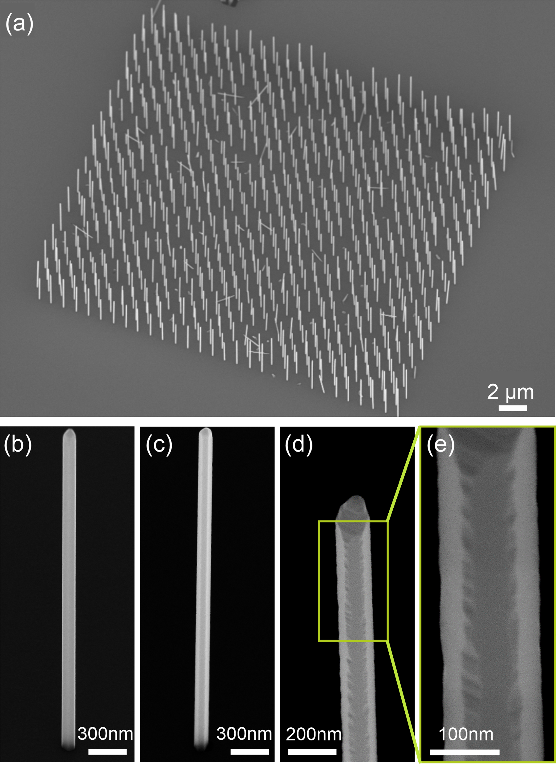
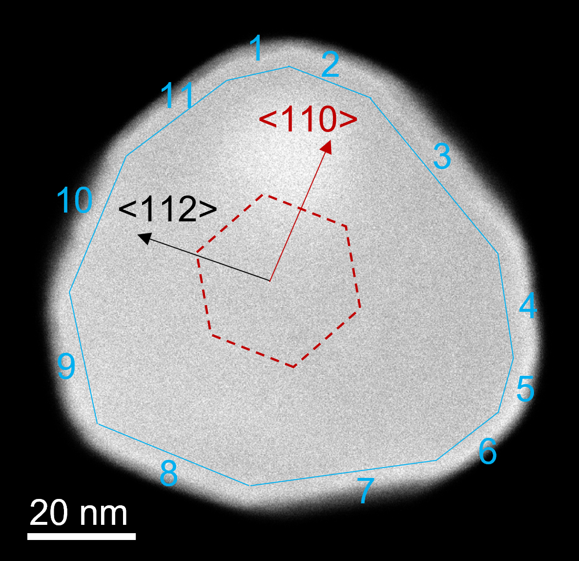
Figure 1 (a) shows a scanning electron microscopy (SEM) image of an array of Te-doped ( cm-3) nanowires (growth run B). The yield is about 95%. The image confirms the uniformity of length and diameter. In Figs. 1 (b) and (c), close-ups of a nanowire from growth runs B and D are shown. Up to a Te concentration of cm-3 the nanowires show a hexagonal cross section with 110 facets as well as a comparable diameter of around 110 nm. However, for the nanowires with the highest Te concentration of cm-3 we observe that diameter increased visibly. Furthermore, as can be clearly seen in Figs. 1 (d) and (e), the sidewalls of the nanowire developed additional {112} facets, forming an irregular dodecagonal shape.
Tellurium atoms have a surfactant effect accumulating on the side facets and decreasing the diffusion length of the host indium atoms.Wixom et al. (2004); Sáfar et al. (1997); Neves et al. (1998) As a result, an increase of the nanowire diameter is expected, which was observed also in our experiments (cf. table 1). A similar behavior has Sb in InAs(Sb) nanowires, where with increasing Sb supply the nanowire radius increases accordingly.Anyebe et al. (2015); Potts et al. (2016)
III.2 Transmissions Electron Microscopy
The crystal structure of the nanowires from all the growths is mainly formed by wurtzite (WZ) region containing inclusions of zinc blende (ZB) segments and twining planes, as shown in Fig. 2 (a) for a nanowire from growth run C. In contrast to the previous study on randomly positioned Te-doped InAs nanowires,Güsken et al. (2019) in these nanowires, no clear clear change in crystal structure was observed with the increase of the Te doping level.
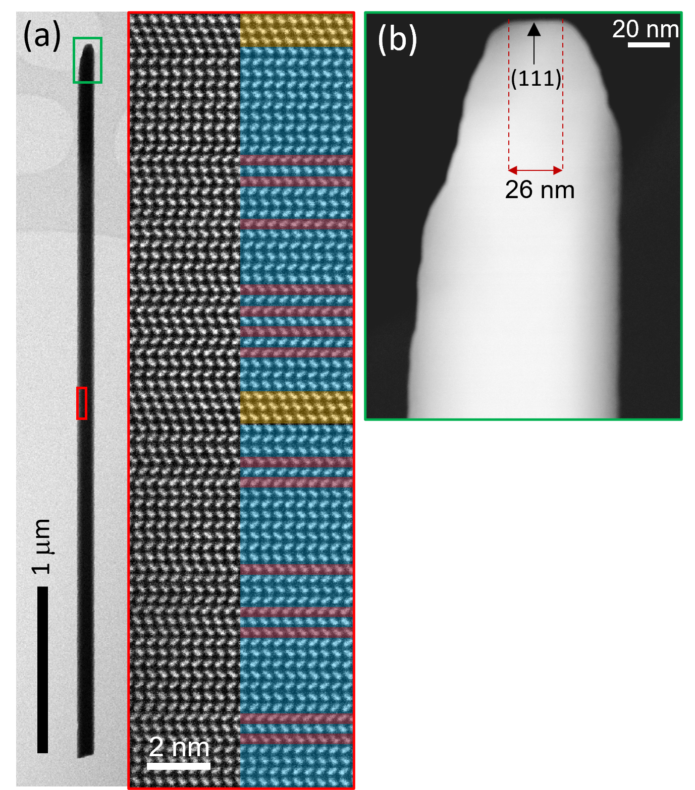
Figure 2 (b) shows a higher magnification image of the tip of the nanowire. Assuming similar facets are maintained during growth, the top (111) growth facet is of smaller diameter than the rest of the nanowire. Therefore, it can be safely assumed that the nanowire growth takes place by adatom deposition on multiple facets on the tip region.
III.3 Atomic Probe Tomography
For APT, single InAs nanowires with different Te doping levels and a GaSb shell are isolated using a method described in detail in Ref. [Koelling et al., 2017]. They are analyzed in a LEAP4000X HR equipment. We imaged the distribution of Te in the InAs nanowires utilizing the same methods for noise level suppression and background correction as in Ref. [Koelling et al., 2017]. The APT analyses reveal four notable findings. First, as can be seen in Fig. 3, Te accumulates at the core of the wire and at the corners of the hexagonal {110} facets for all investigated Te doping concentrations.
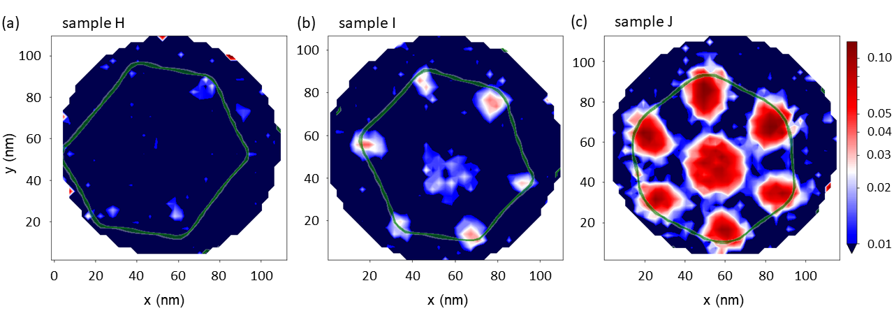
Second, the measured Te dopant incorporation increases with the corresponding nominal doping (cf. Figs. 3 and 4). Third, the Te concentration increases towards the bottom of the nanowires typically reaching a factor of higher concentration near the bottom with respect to the top (cf. Fig. 4). Forth, as depicted in Fig. 5, with the increase of Te nominal doping, the facets of the hexagonal InAs nanowires become unstable and the nanowires with the highest doping have locally dodecagonal cross sections. This observation is confirmed by TEM cross sectional images, as shown in Supplemental Material Fig. S1.
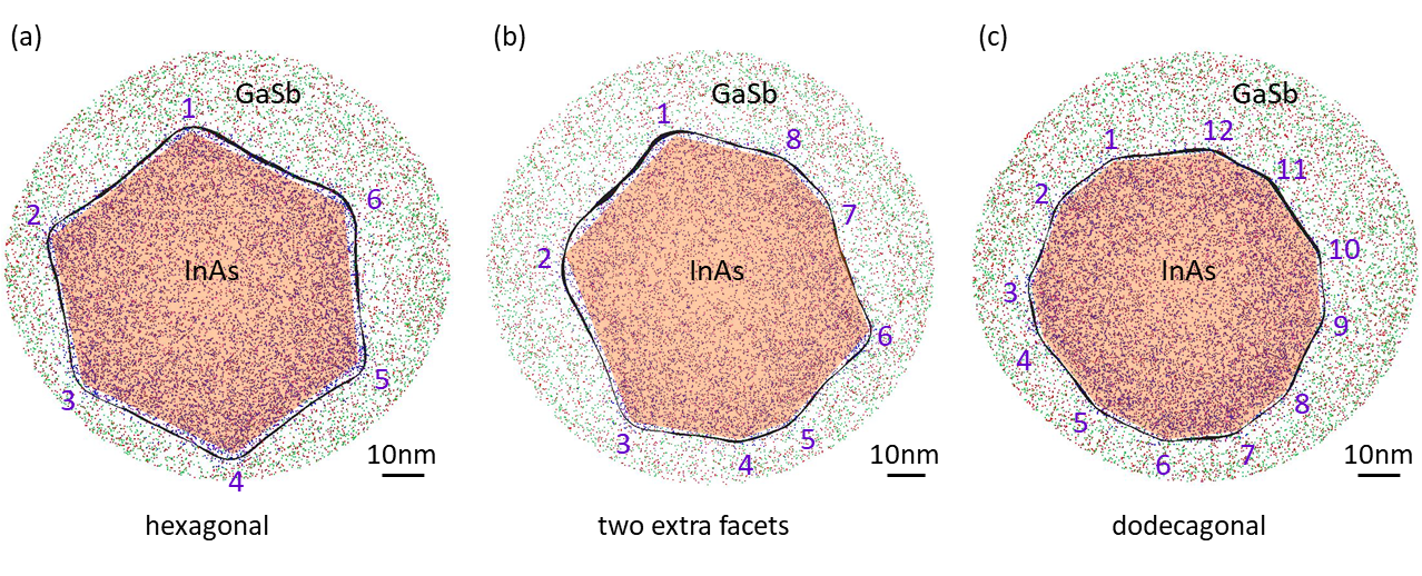
We interpret these findings as follows. Te diffuses along the sidewall of the nanowire, a contribution coming also from the substrate surface, and incorporates via the small (111) growth facet on the top of the nanowire (Fig. 2 (b)) and on the corners of the hexagonal facets. Note that the diameters of the top (111) facet in Fig. 2 (b) and the Te rich core in Fig. 3 (c) are comparable. As the wire grows, the diffusion contribution of the substrate surface disappear and Te incorporation at top decreases. Due to the large covalent radius of Te atoms, they accumulate on the corners between facets. The accumulation at the corners promotes the formation of (112) facets and hence the dodecagonal segments. One can presume that the surfactant Te incorporates easier into the solid on (111) and (112) surfaces than (110).
III.4 Electrical Characterization
In Fig. 6 the resistance at room temperature from nanowires with different doping levels are plotted function of the ratio of nominal distance between the contacts and the cross sectional area .
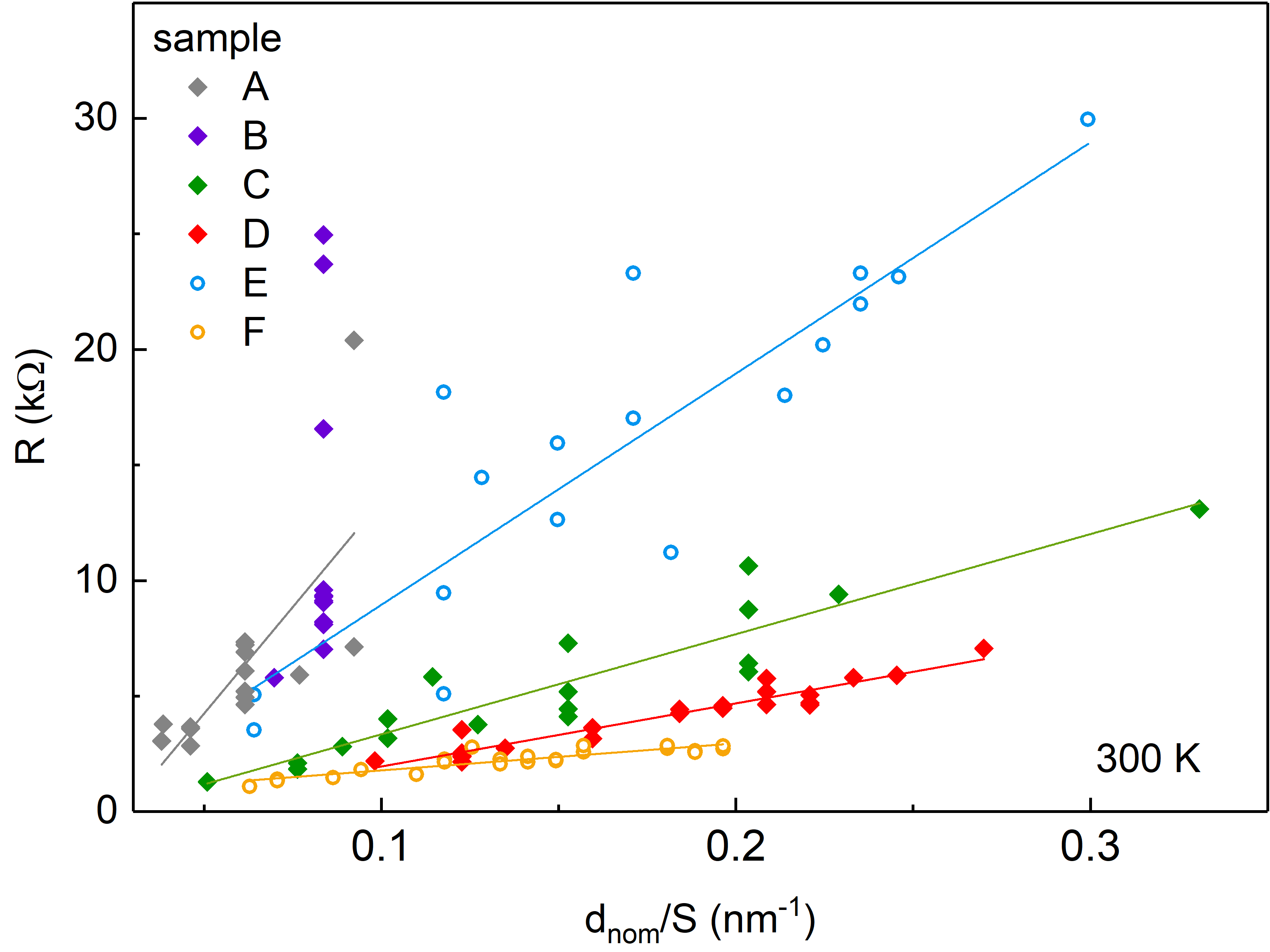
Here, was determined for each growth series by average the diameters of the measured nanowires assuming a regular hexagonal shape. The transport measurements have been carried out in a four-terminal scheme in order to eliminate the effect of contact resistances. For each growth run with a specific doping concentration, one finds a linear increase of resistance with the contact separation length verifying the ohmic behavior of the transport in the wire. The doping effect of Te is confirmed by the decrease of the slope, i.e. decreased resistivity , with increasing doping concentration (c.f. Table 1). In Fig. 6 one observes that there is a spread of the resistance of different nanowires with identical contact separation. The effect is less pronounced for higher doping levels. One reason for the varying conductance could be found in non-uniform cross section . Although the nanowires were grown in a selective-area epitaxy scheme, fluctuations of the cross sectional area can not be avoided.
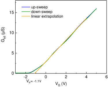
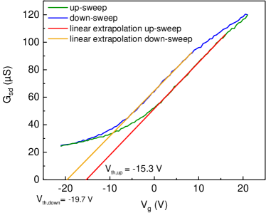
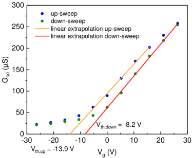
Charge carrier concentrations of nanowires with different doping levels were extracted from field-effect measurements by biasing a global back gate. We found that the conductance is reduced for negative gate voltages, confirming the -type doping character. Quantitative information about charge carrier concentration was obtained using the threshold voltage at pinch-off. Since nanowires with a Te doping concentration larger than did not reach pinch-off at accessible back-gate voltages, was in this case obtained by extrapolating the approximately linear dependence towards positive voltages. Example of traces including a linear fit are given in the Supplemental Material in Figs. S2 - S4. Some nanowire samples showed a gate hysteresis behavior, which was reproducible during several cycles. In that case, was determined by taking the average of the threshold voltages for up- and down-sweeps. Details of the determination of and the calculation of the charge carrier concentration are given in the Supplemental Material.
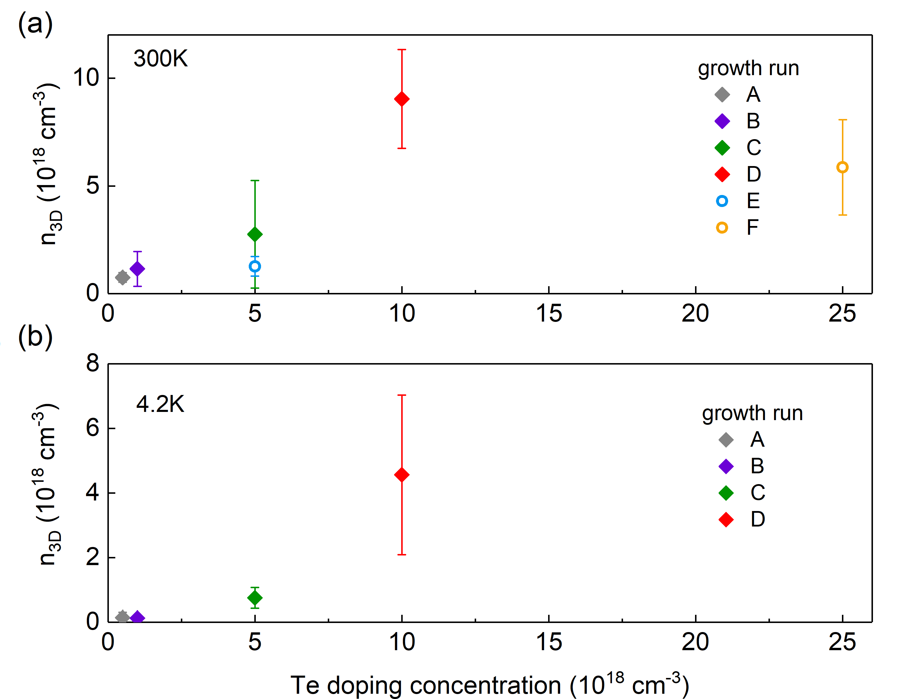
The field-effect measurements on nanowires grown with different Te doping concentrations were carried out at room temperature and at 4.2 K. The corresponding charge carrier concentrations at different nominal doping concentrations are depicted in Fig. 7. The graphs confirm that the experimentally determined charge carrier concentration values increase with the nominal doping of the nanowires.
For sample C and D, one finds that at room temperature, the measured carrier concentrations are close to the nominal Te doping concentrations demonstrating the efficient dopant incorporation. However, for samples E and F grown with the low As4 flux the doping efficiency is somewhat lower, the obtained charge carrier concentrations being lower than expected from the previous growth runs A to D. This could be explained by a modified Te incorporation due to altered growth conditions by decreased As4 flux. The measured charge carrier concentrations are found to be generally higher at room temperature compared with 4.2 K, which represents the expected behavior in semiconductors.
A relatively large spread of for the investigated nanowires from identical batches is observed. A possible explanation for that is the imprecise character of the method to determine the charge carrier concentration from the gate pinch-off threshold voltage. Defects within the oxide and at the interface with the semiconductor effectively alter the capacitance used to determine the carrier concentration (see section II-B in the Supplemental Material) leading to scattered results. Furthermore, it was shown in Fig. 4 that the Te incorporation along the nanowire axis is not uniform, resulting in different effective doping depending on the length of the particular nanowire. Therefore, one must be careful to directly compare the obtained results with measurements from APT. However, it can be concluded that the charge carrier concentration strongly depends on the nominal dopant concentration, suggesting an effective -type doping of InAs by Te.
III.5 Josephson junctions
In order to demonstrate the suitability of Te-doped nanowires for superconducting hybrid structures the properties of gate-controlled Josephson junctions are investigated. The measurements have been performed in a 3He/4He dilution refrigerator with a base temperature of 15 mK. The measured junctions JJ-A, JJ-B, and JJ-D were fabricated from nanowires from growth series A, B, and D, respectively. A typical structure is shown in Fig. 8 (a), in which the nanowire-based Josephson junction is shunted by an AuGe resistor.
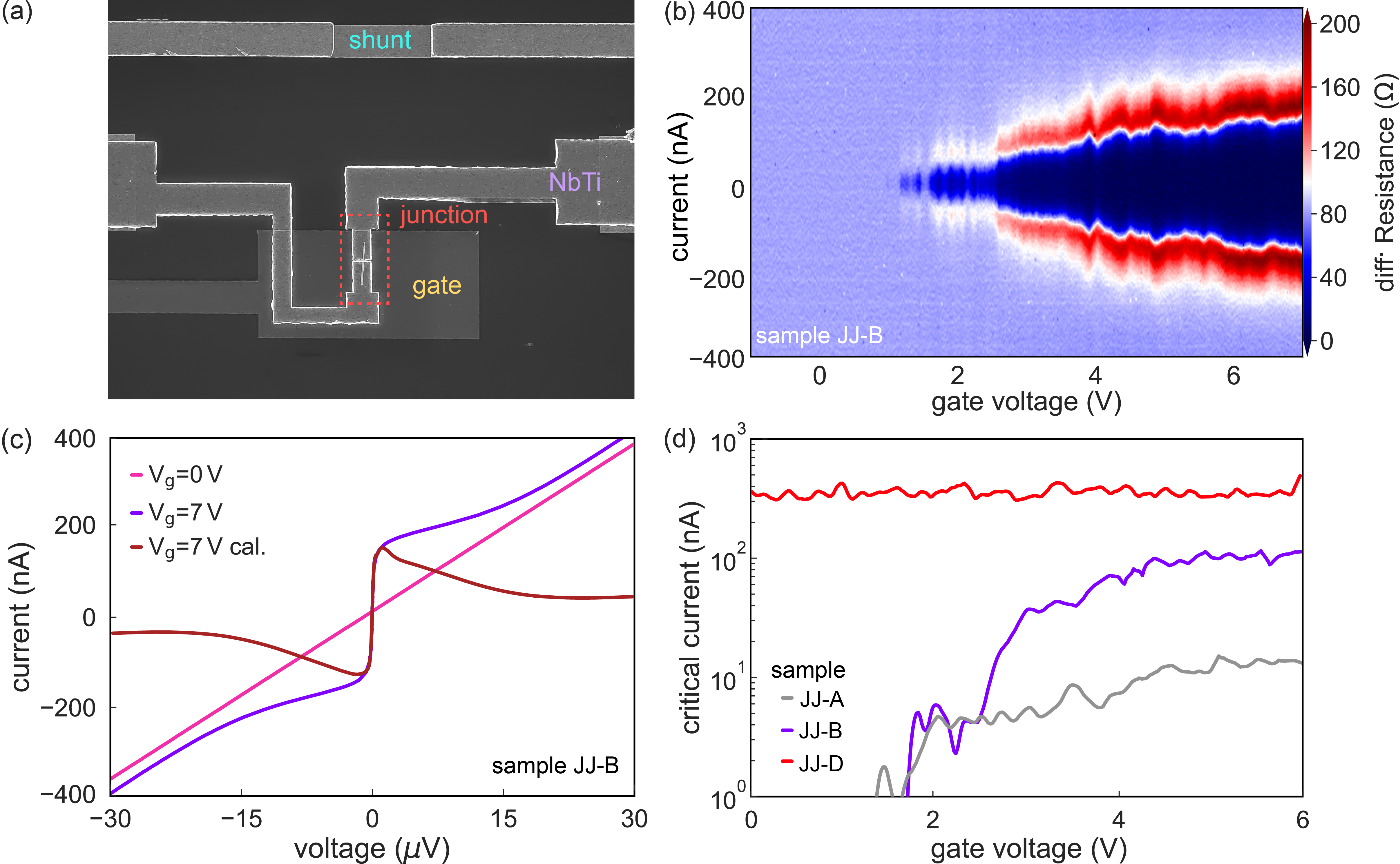
The shunt was included to suppress hysteretic effects in the current-voltage characteristics and to improve the performance of the device in measurements of the ac-Josephson effect Joyez et al. (1999); Chauvin (2005). In Fig. 8 (b) the color-coded differential resistance vs. bias current is plotted in the gate voltage range from V to 7 V for junction JJ-B made from a nanowire having a doping nominal concentration of cm-3. One finds that for gate voltages below V the nanowire is pinched off, with the remaining resistance of 80 given by the shunt resistor. Between =V and V the device shows signatures of Coulomb blockade which can be attributed to the presence of an intrinsic quantum dot.Zellekens et al. (2020) At gate voltages above V, the nanowire channel is open and exhibits gate-tunable supercurrent, i.e., an important requirement for hybrid superconducting circuit applications. The critical current shows some superimposed fluctuations due to interference effects.Doh et al. (2005); Günel et al. (2012) From Fig. 8 (c) showing a single voltage-current () trace at V (red curve) a critical current of nA is extracted. The characteristics contains the contribution of the shunt resistor, which needs to be subtracted to gain the actual current through the junction. Indeed, the resistance of the shunt can be determined directly from the measurement at zero gate voltage (cf. Fig. 8 (c)), where the junction is pinched-off completely. After the calibration of the junction response by means of a point-wise combination of the traces at V and V, it is possible to extract the unperturbed characteristics of the device (cf. Fig. 8 (c), dark red trace). Junctions JJ-A and JJ-B could be pinched-off completely so that the normal state resistance could be extracted. At a gate bias of V we determined products of 65 V and V for sample JJ-A and JJ-B, respectively.
The critical current as a function of gate voltage for all investigated Josephson junctions are shown in Fig. 8 (d). The junction containing a nanowire with the highest doping level only shows a weak relation between and the measured . In contrast, the wires with the lower carrier concentrations exhibit a transistor-like behavior with pronounced pinch-off and saturation regions. All critical currents shown some fluctuations due to inference effects in the nanowire channel.Doh et al. (2005); Günel et al. (2012) The difference in the threshold voltage between junction JJ-A and JJ-B are attributed to Coulomb resonances which dominate the transport at low gate values.Zellekens et al. (2020) A comparison of the critical current at V reveals increase by a factor of 10 between JJ-A and JJ-B and a factor of five between JJ-B and JJ-D, which confirms the impact of the doping concentration on .
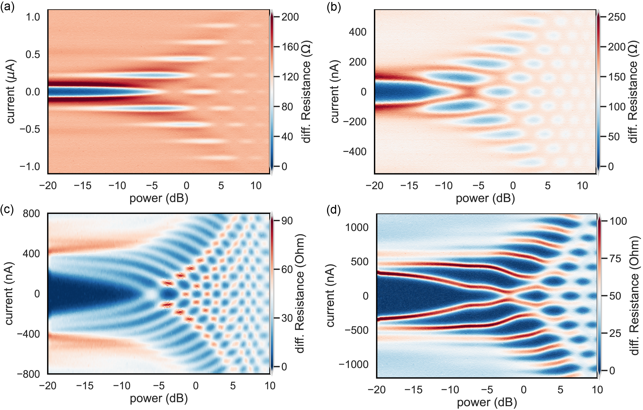
A reliable way to confirm that nanowire-based junction do indeed carry a Josephson supercurrent is to perform measurements under microwave irradiation. Here, the application of a microwave signal results in Shapiro steps of height , with , Planck constant and . Figure 9 (a) shows a set of current–voltage traces of junction JJ-D for GHz and different microwave powers at V.
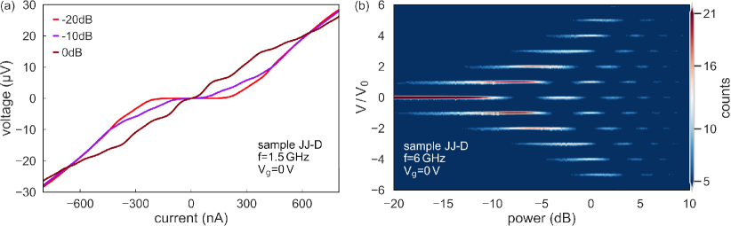
At low power, i.e. dB, the curve basically mimics the behavior of a purely DC-driven junction. However, if the power is increased to dB and further to dB, the zero voltage state is gradually suppressed and equidistant voltage plateaus, i.e. Shapiro steps, appear. In Fig. 9 (b) the presence of Shapiro steps at multiples of for GHz is shown as a function of microwave power. The color scale gives the number of counts as a function of voltage, i.e. large number of count corresponds to the appearance of a step. The regular oscillating pattern without any subharmonic features indicates a sinusoidal current-phase relation of the Josephson junction.
IV Conclusions
We demonstrate that Te is an efficient dopant for MBE-grown InAs nanowires. At very high dopant concentrations, above cm-3, a change in wire morphology was observed, where the hexagonal cross section changes to a dodecagonal one. The side facets have also a great influence on the distribution of Te dopant, which accumulates at the corners of the hexagonal (111) facets,as APT revealed. In addition, the APT showed that in the center of the wire the Te concentration is higher and that the total Te concentration increases toward the bottom of the nanowire. The effective doping was confirmed by electrical measurements at room temperature and 4 K, where a systematic increase in the conductivity of the wire with the doping concentration was observed. Indeed, a significant increase in the critical current was obtained in Josephson junctions with a nanowire weak link. At moderate doping concentrations, even gate control was maintained. Since InAs nanowires are often used in hybrid structures for Majorana physics or quantum computing, Te doping provides a very efficient method to tailor the nanowire properties for devices in these applications.
Acknowledgements
We thank Tobias Ziegler, Patrick Liebisch, Patrick Pilch, Bram Aarts and Abbas Espiari for their assistance during sample preparation and Michael Schleenvoigt for the metal deposition, Marvin Jansen for initial assistance with TEM, Benjamin Bennemann, Christoph Krause, and Herbert Kertz for technical assistance. Dr. Florian Lentz and Dr. Stefan Trellenkamp are gratefully acknowledged for electron beam lithography. Dr. Elmar Neumann and Stephany Bunte for their assistance with the focused ion beam setup and scanning electron microscopy. Dr. Gianluigi Catelani is gratefully acknowledged for theory support regarding the magnetic field measurements. All samples have been prepared at the Helmholtz Nano Facility.Forschungszentrum Jülich GmbH (2017) The work at Forschungszentrum Jülich was partly supported by the project ”Scalable solid state quantum computing”, financed by the Initiative and Networking Fund of the Helmholtz Association, by the Deutsche Forschungsgemeinschaft (DFG, German Research Foundation) Project: ”Coupling of quantum dots with superconductors”, (SCHA 835/9-1), UK EPSRC is acknowledged for funding through grant No. EP/P000916/1. The APT work was supported by NSERC Canada (Discovery, SPG, and CRD Grants), Canada Research Chairs, Canada Foundation for Innovation, Mitacs, PRIMA Québec, and Defence Canada (Innovation for Defence Excellence and Security, IDEaS). The work at RIKEN was partially supported by Grant-in-Aid for Scientific Research (B) (No. 19H02548), Grants-in-Aid for Scientific Research (S) (No. 19H05610), and Scientific Research on Innovative Areas ”Science of hybrid quantum systems” (No. 15H05867).
References
- Dayeh et al. (2007) S. Dayeh, D. P. Aplin, X. Zhou, P. K. Yu, E. Yu, and D. Wang, Small 3, 326 (2007).
- Tomioka et al. (2007) K. Tomioka, P. Mohan, J. Noborisaka, S. Hara, J. Motohisa, and T. Fukui, J. Cryst. Growth 298, 644 (2007).
- Thelander et al. (2008) C. Thelander, C. Rehnstedt, L. E. Froberg, E. Lind, T. Martensson, P. Caroff, T. Lowgren, B. J. Ohlsson, L. Samuelson, and L.-E. Wernersson, Electron Devices, IEEE Transactions on 55, 3030 (2008).
- Burke et al. (2015) A. M. Burke, D. J. Carrad, J. G. Gluschke, K. Storm, S. Fahlvik Svensson, H. Linke, L. Samuelson, and A. P. Micolich, Nano Letters 15, 2836 (2015).
- Fasth et al. (2005) C. Fasth, A. Fuhrer, M. T. Bjork, and L. Samuelson, Nanoletters 5, 1487 (2005).
- Fuhrer et al. (2007) A. Fuhrer, L. E. Fröberg, J. N. Pedersen, M. W. Larsson, A. Wacker, M.-E. Pistol, and L. Samuelson, Nano Letters 7, 243 (2007).
- Heedt et al. (2016) S. Heedt, A. Manolescu, G. A. Nemnes, W. Prost, J. Schubert, D. Grützmacher, and T. Schäpers, Nano Letters 16, 4569 (2016).
- Heedt et al. (2017) S. Heedt, N. T. Ziani, F. Crépin, W. Prost, J. Schubert, D. Grützmacher, B. Trauzettel, T. Schäpers, et al., Nature Physics 13, 563 (2017).
- Iorio et al. (2019) A. Iorio, M. Rocci, L. Bours, M. Carrega, V. Zannier, L. Sorba, S. Roddaro, F. Giazotto, and E. Strambini, Nano Letters 19, 652 (2019).
- Bordoloi et al. (2020) A. Bordoloi, V. Zannier, L. Sorba, C. Schönenberger, and A. Baumgartner, Communications Physics 3, 1 (2020).
- Mourik et al. (2012) V. Mourik, K. Zuo, S. M. Frolov, S. R. Plissard, E. P. A. M. Bakkers, and L. P. Kouwenhoven, Science 336, 1003 (2012).
- Aguado (2017) R. Aguado, Rivista del Nuova Cimento 40, 523 (2017).
- Doh et al. (2005) Y.-J. Doh, J. A. van Dam, A. L. Roest, E. P. A. M. Bakkers, L. P. Kouwenhoven, and S. D. Franceschi, Science 309, 272 (2005).
- Günel et al. (2012) H. Y. Günel, I. E. Batov, H. Hardtdegen, K. Sladek, A. Winden, K. Weis, G. Panaitov, D. Grützmacher, and T. Schäpers, Journal of Applied Physics 112, 034316 (2012).
- Larsen et al. (2015) T. W. Larsen, K. D. Petersson, F. Kuemmeth, T. S. Jespersen, P. Krogstrup, J. Nygård, and C. M. Marcus, Phys. Rev. Lett. 115, 127001 (2015).
- de Lange et al. (2015) G. de Lange, B. van Heck, A. Bruno, D. J. van Woerkom, A. Geresdi, S. R. Plissard, E. P. A. M. Bakkers, A. R. Akhmerov, and L. DiCarlo, Phys. Rev. Lett. 115, 127002 (2015).
- Zazunov et al. (2003) A. Zazunov, V. S., Shumeiko, E. N. Bratus, J. Lantz, and G. Wendin, Phys. Rev. Lett. 90, 087003 (2003).
- Wieder (1974) H. H. Wieder, Applied Physics Letters 25, 206 (1974).
- Sladek et al. (2010) K. Sladek, V. Klinger, J. Wensorra, M. Akabori, H. Hardtdegen, and D. Grützmacher, Journal of Crystal Growth 312, 635 (2010).
- Wirths et al. (2011) S. Wirths, K. Weis, A. Winden, K. Sladek, C. Volk, S. Alagha, T. E. Weirich, M. von der Ahe, H. Hardtdegen, H. Lüth, N. Demarina, D. Grützmacher, and T. Schäpers, Journal of Applied Physics 110, 053709 (2011).
- Ghoneim et al. (2012) H. Ghoneim, P. Mensch, H. Schmid, C. D. Bessire, R. Rhyner, A. Schenk, C. Rettner, S. Karg, K. E. Moselund, H. Riel, and M. T. Björk, Nanotechnology 23, 505708 (2012).
- Dimakis et al. (2013) E. Dimakis, M. Ramsteiner, C.-N. Huang, A. Trampert, A. Davydok, A. Biermanns, U. Pietsch, H. Riechert, and L. Geelhaar, Applied Physics Letters 103, 143121 (2013).
- Park et al. (2015) D. W. Park, S. G. Jeon, C.-R. Lee, S. J. Lee, J. Y. Song, J. O. Kim, S. K. Noh, J.-Y. Leem, and J. S. Kim, Scientific Reports 5 (2015), 10.1038/srep16652.
- Sankaran (1980) R. Sankaran, Journal of Crystal Growth 50, 859 (1980).
- Kamp et al. (1994) M. Kamp, G. Mörsch, J. Gräber, and H. Lüth, Journal of Applied Physics 76, 1974 (1994).
- Bennett et al. (2003) B. R. Bennett, R. Magno, and N. Papanicolaou, Journal of crystal growth 251, 532 (2003).
- Wallentin and Borgström (2011) J. Wallentin and M. T. Borgström, Journal of Materials Research 26, 2142 (2011).
- Orrù et al. (2016) M. Orrù, E. Repiso, S. Carapezzi, A. Henning, S. Roddaro, A. Franciosi, Y. Rosenwaks, A. Cavallini, F. Martelli, and S. Rubini, Advanced Functional Materials 26, 2836 (2016).
- Goktas et al. (2018) N. I. Goktas, E. M. Fiordaliso, and R. R. LaPierre, Nanotechnology 29, 234001 (2018).
- Hakkarainen et al. (2019) T. Hakkarainen, M. Rizzo Piton, E. M. Fiordaliso, E. D. Leshchenko, S. Koelling, J. Bettini, H. Vinicius Avan ço Galeti, E. Koivusalo, Y. G. a. Gobato, A. de Giovanni Rodrigues, D. Lupo, P. M. Koenraad, E. R. Leite, V. G. Dubrovskii, and M. Guina, Phys. Rev. Materials 3, 086001 (2019).
- Güsken et al. (2019) N. A. Güsken, T. Rieger, G. Mussler, M. I. Lepsa, and D. Grützmacher, Nanoscale Research Letters 14, 179 (2019).
- Koblmüller et al. (2010) G. Koblmüller, S. Hertenberger, K. Vizbaras, M. Bichler, F. Bao, J.-P. Zhang, and G. Abstreiter, Nanotechnology 21, 365602 (2010).
- Perla et al. (2021) P. Perla, H. A. Fonseka, P. Zellekens, R. Deacon, Y. Han, J. Kölzer, T. Mörstedt, B. Bennemann, A. Espiari, K. Ishibashi, et al., Nanoscale Advances 3, 1413 (2021).
- Rieger et al. (2013) T. Rieger, D. Grützmacher, and M. I. Lepsa, physica status solidi (RRL)–Rapid Research Letters 7, 840 (2013).
- Wixom et al. (2004) R. Wixom, L. Rieth, and G. Stringfellow, Journal of crystal growth 269, 276 (2004).
- Sáfar et al. (1997) G. A. M. Sáfar, W. N. Rodrigues, L. A. Cury, H. Chacham, M. V. B. Moreira, S. L. S. Freire, and A. G. de Oliveira, Applied Physics Letters 71, 521 (1997).
- Neves et al. (1998) B. R. A. Neves, M. S. Andrade, W. N. Rodrigues, G. A. M. Sáfar, M. V. B. Moreira, and A. G. de Oliveira, Applied Physics Letters 72, 1712 (1998).
- Anyebe et al. (2015) E. Anyebe, M. K. Rajpalke, T. D. Veal, C. Jin, Z. Wang, and Q. Zhuang, Nano Research 8, 1309 (2015).
- Potts et al. (2016) H. Potts, M. Friedl, F. Amaduzzi, K. Tang, G. Tütüncüoglu, F. Matteini, E. Alarcon Lladó, P. C. McIntyre, and A. Fontcuberta i Morral, Nano letters 16, 637 (2016).
- Koelling et al. (2017) S. Koelling, A. Li, A. Cavalli, S. Assali, D. Car, S. Gazibegovic, E. P. A. M. Bakkers, and P. M. Koenraad, Nano Letters 17, 599 (2017).
- Hellman et al. (2003) O. C. Hellman, J. B. du Rivage, and D. N. Seidman, Ultramicroscopy 95, 199 (2003), iFES 2001.
- Joyez et al. (1999) P. Joyez, D. Vion, M. Götz, M. Devoret, and D. Esteve, Journal of superconductivity 12, 757 (1999).
- Chauvin (2005) M. Chauvin, The Josephson effect in atomic contacts, Ph.D. thesis, Université Pierre et Marie Curie-Paris VI (2005).
- Zellekens et al. (2020) P. Zellekens, R. Deacon, P. Perla, H. A. Fonseka, T. Mörstedt, S. A. Hindmarsh, B. Bennemann, F. Lentz, M. I. Lepsa, A. M. Sanchez, D. Grützmacher, K. Ishibashi, and T. Schäpers, Phys. Rev. Applied 14, 054019 (2020).
- Forschungszentrum Jülich GmbH (2017) Forschungszentrum Jülich GmbH, Journal of large-scale facilities 3, A112 (2017).
Te-doped selective-area grown InAs nanowires for superconducting hybrid devices (Supplemental Material)
SI TEM cross-section images showing nanowires facets
In Fig. S1 a cross section of a nanowire from growth run F is depicted.
SII Electrical Characterization
A Electrical characterization of Te-doped nanowires
Electrical characterisation of nanowires with varying Te-doping levels were performed at room temperature as well as at 4.2 K. Room temperature measurements without back gate were done using a Keithley SCS-4200 semiconductor characterisation system connected to a 4-point probe station. Measurements at low temperature were performed in a Lakeshore liquid 4He flow-cryostat capable of cooling down to approximately 4.0 K. Nanowires were investigated in two- and four-terminal configurations with and without applying a voltage to the back gate. A Keithley 2636B source-measurement unit was used for the application of the bias current. Potential differences in four-terminal configuration were measured using a Keysight 34461A multimeter with input impedance of 10 M.
B Determination of carrier concentration
In order to obtain information on charge carrier density in the nanowires, the source-drain conductance was investigated depending on voltage applied to the global back-gate electrode. The threshold voltage was extracted by extrapolating from the linear behavior at positive gate voltages (cf. Fig. S2). Some gate-dependent measurements showed an hysteresis effect, i.e. the results for gate up- and down-sweep were slightly shifted. In these cases, the average value was used for further evaluation (c.f. Figs. S3 and S4). Gate-dependent measurements were achieved on two ways. On the one hand, the gate was swept by directly taking the source-drain current at constant . Alternatively, the conductance was extracted from sweeps at different fixed gate voltages. This was preferred in cases with a small gate hysteresis, in order to reduce uncertainties in conductance from offsets of the measurement devices. In Fig. S4 an example measurement for the latter case is shown.
For calculating the charge carrier concentration from the threshold voltages the following relation was usedDayeh et al. (2007)
| (S1) |
with the electron charge, the nanowire length between the contacts, its radius. denotes the capacitance between the nanowire and the global back-gate electrode. It is given byDayeh et al. (2007)
| (S2) |
Here, is the dielectric constant, is the relative dielectricity of the gate oxide, i.e. for SiO2, denotes the thickness of the oxide between back-gate and nanowire and the diameter of the nanowire.
SIII Extrinsically shunted Josephson junctions
In Josephson junctions the dissipationless supercurrent arises from the coherent tunneling of Cooper pairs between two superconducting electrodes, driven by the phase difference . In tunnel junctions with large spatial extensions, the phase can be considered as a quasistatic parameter due to the damping effect of the large capacitance associated with it. The large time constant suppresses sudden changes of the voltage , which stabilizes the system with respect to thermal and quantum fluctuations. However,if one assumes a nanowire Josephson junction, the phase dynamics are not longer purely determined by the superconductor/nanowire/superconductor stack itself. Instead, the superconducting leads and the circuit environment, modeled as a admittance , with the frequency, start to influence the electromagnetic properties of the device. Thus, the phase difference between the two superconducting electrodes of the junction is not a simple parameter anymore rather than the combination of all phase fluctuation contributionsJoyez et al. (1999); Chauvin (2005)
| (S3) |
Here, corresponds to the von-Klitzing constant (), is the electron temperature and is the total impedance. The latter is thereby determined by the junction inductance , the junction capacitance and the impedance of the external circuit. In case of a small junction, and are small, too, and is dominated by the external circuit admittance . Such a scenario is usually associated with large phase fluctuations, which ultimately lead to a stochastic behavior of the corresponding supercurrent:
| (S4) |
e.g. a widely spread distribution of the switching current or the occurrence of a hysteresis in the zero-voltage state. The latter is especially important in the case of large supercurrents, for which the actual electron temperature deviates significantly from the bath temperature due to overheating effects.Courtois et al. (2008)
The most simple way to limit both phase noise as well as phase diffusion is the implementation of an on-chip shunt resistor in close proximity to the nanowire Josephson junctions.Joyez et al. (1999); Chauvin (2005) In our case, the InAs/Al half-shell nanowire Josephson junction is shunted by an on-chip AuGe stripe (cf. Fig. 8 (a) in the main text) Both elements are connected by superconducting TiN electrodes. The normal conducting shunt resistor causes as suppression of the pronounced and abrupt switch between zero voltage state and dissipative transport. Instead, there is a smooth and continuous transition between both branches, effectively providing experimental access to the full voltage range. After the subtraction of the shunt resistance, the remaining trace exhibits the typical decrease of the current above a critical value, which is a clear signature for the suppression of the Cooper pair driven transport. By extracting the turning point of the supercurrent peak, as shown in, it is then possible to obtain the maximum junction current .Joyez et al. (1999); Chauvin (2005)
The full calibration procedure is as follows: First, the gate dependency of the supercurrent is investigated in order to measure the shunt resistor independently. Thus, the nanowire has to be pushed into pinch-off by applying a sufficiently large negative gate voltage. Now, by applying a linear fit within the range of the supercurrent branch to every individual - characteristics, it is possible to obtain the combined resistance of the parallel circuit. For negative voltages, i.e. when the nanowire is pinched-off, the circuit resistance becomes equal to the normal conducting shunt resistance. In order to limit the influence of noise and measurement uncertainties, the whole saturation region is used to calculate an average value for the resistor. The contribution of the normal conducting shunt resistor, which acts as an additive and linear contribution, can then be removed by a point-wise extraction of the junction resistance and calibration of the measured voltage
| (S5) | |||||
| (S6) |
with as the externally applied current.
SIV Shapiro measurements on nanowire Josephson junctions with different doping concentrations
Figure S5 provides an overview of the power-dependent Shapiro response for the junctions JJ-A and JJ-D in the main manuscript. For the undoped nanowires, a pronounced spectrum can be observed for both measurements, i.e. f = 4.1 GHz (cf. Fig. S5 (a)) and f = 6.0 GHz (cf. Fig. S5 (b)), respectively. Thus, even though the nanowire have a low carrier concentration and despite the comparably poor quality of the ex-situ contacts, a clear supercurrent without any resistive contribution can be observed if a sufficiently large gate voltage (V4 V) is applied. The same holds for the wires with the highest doping level in Figs. S5 (c) and (d), respectively, proving that the large supercurrent of I200 nA is really carried by a Josephson junction rather than just a metallic short.
References
- Dayeh et al. (2007) S. Dayeh, D. P. Aplin, X. Zhou, P. K. Yu, E. Yu, and D. Wang, Small 3, 326 (2007).
- Joyez et al. (1999) P. Joyez, D. Vion, M. Götz, M. Devoret, and D. Esteve, Journal of superconductivity 12, 757 (1999).
- Chauvin (2005) M. Chauvin, The Josephson effect in atomic contacts, Ph.D. thesis, Université Pierre et Marie Curie-Paris VI (2005).
- Courtois et al. (2008) H. Courtois, M. Meschke, J. T. Peltonen, and J. P. Pekola, Physical Review Letters 101, 067002 (2008).